Self-aligned fiber-based dual-beam source for STED nanolithography  Download: 811次
1. Introduction
Nanolithography is playing an increasingly important role in modern society. However, due to the limitation of Abbe’s diffraction, the feature size by single-beam lithography cannot exceed half a wavelength. Inspired by stimulated emission depletion (STED) microscopy[1], which has been widely used in micro-imaging[2], dual-beam STED lithography has become a simple and effective way to break through the diffraction limit. The main principle is that the hollow depletion beam can inhibit the polymerization reaction between the excitation beam and the photosensitive material, and only the hollow part in the middle allows the excitation beam for direct laser writing, thereby realizing lithography that breaks the diffraction limit[3]. Since STED lithography can easily realize arbitrary two-dimensional (2D) or three-dimensional (3D) structures[4], it would be highly desirable in biotechnology[5,6] and photonic devices[7
In this article, a customized vortex fiber is used to generate and coaxially align the depletion beam and the excitation beam employed in STED nanolithography. More details of the vortex fiber can be found in Refs. [22,23]. The lasers with wavelengths of 1030 nm and 532 nm are coupled into the vortex fiber simultaneously. The near-infrared pulsed laser is usually used as the excitation beam source in lithography technology, which is mainly due to the low photon energy in this wavelength range and good penetrability of materials. The continuous-wave (CW) 532 nm fundamental Gaussian mode is converted into ring-shaped mode by the vortex fiber, which is adopted as the depletion beam for STED lithography. Meanwhile, the vortex fiber maintains the characteristics of a pulsed 1030 nm fundamental mode with controllable polarization as the excitation beam for STED lithography. With the self-alignment provided by the fiber, it is simple to maintain the two beams to be strictly coaxial. The Stokes parameter measurement for the two beams are used to simulate point spread function (PSF) of each beam within the focal region and calculate the effective spot size for the dual-beam STED nanofabrication.
2. Experiments
The schematic diagram of fiber-based STED nanolithography setup is shown in Fig. 1. A home-built fiber laser[24,25] is employed to generate a pulse laser with a central wavelength of 1030 nm, whose polarization is adjusted with a half-wave plate (HWP). The polarization of the 532 nm CW laser is controlled by an HWP and a quarter-wave plate. The dichroic mirror (DMLP805, Thorlabs) is used to transmit the 1030 nm beam and reflect the 532 nm beam, and the two beams are brought to roughly coincide in space by adjusting the propagation directions of the two beams with mirror pairs. The carefully selected lens L is exploited to focus both of them into a spot size of about 2 µm, which is equivalent to the core size of the vortex fiber. The nanometer translation stage (NanoMax 300, Thorlabs) is used to adjust the position of the optical fiber so that two beams can be coupled into the single-mode fiber at the same time with high efficiency.

Fig. 1. Schematic diagram of fiber-based STED nanolithography setup. (HWP, half wave plate; QWP, quarter wave plate; DM, dichroic mirror; L, lens; SMF, single-mode fiber; BFG, Bragg fiber grating; LPG, long-period grating; PC, polarization controller.)
The single-mode fiber transmits two beams to the Bragg grating, which converts the 532 nm laser into high-order modes while maintaining the 1030 nm laser in the fundamental mode. The Bragg grating couples two beams into the vortex fiber with the refractive index of its core in ring-shaped distribution. This customized fiber could increase the effective refractive index difference between adjacent high-order modes, realizing the generation of a polarization vortex beam. An azimuthally polarized 532 nm beam ( mode) is selected by the tilted long-period grating in the vortex fiber, while the intensity distribution of 1030 nm laser is maintained as unchanged. Subsequently, the 1030 nm Gaussian mode pulsed laser is utilized as an excitation beam, and the donut-shaped 532 nm laser is exploited as the depletion beam required by STED lithography. Due to the self-alignment offered by the optic fiber, the output excitation beam and depletion beam are strictly coaxial.
3. Results and Discussion
First, we block the 532 nm laser and adjust the 1030 nm beam to vertical polarization by rotating the HWP. A quarter-wave plate and a polarizer are placed behind the fiber tail to measure the Stokes parameters of the excitation beam with the power of 6 mW. The polarization, frequency spectrum, pulse sequence, and pulse width of the excitation beam are measured in front of and behind the vortex fiber to check whether the fiber will cause any changes to the laser pulse. The measured results are shown in Figs. 2 and 3. According to the comparison between Figs. 2(a) and 2(b), the intensity distribution of the 1030 nm beam is still the Gaussian distribution, but its polarization is changed from the vertical to horizontal direction. The spectrum width of the input pulsed beam is about 20 nm, and its central wavelength is 1030 nm [Fig. 2(c)]. The spectrum of the output beam after the vortex fiber remains almost unchanged, and the central wavelength is still 1030 nm [Fig. 2(d)]. According to the measured input and output pulse sequences [Figs. 3(a) and 3(b)], the repetition frequency of 1030 nm laser remains consistent at 52.6 MHz. From Fig. 3(c), we can see that the pulse width of the 1030 nm laser is 1.2 ps. The experiments prove that the vortex fiber brings negligible changes to the characteristics of the pulsed 1030 nm laser. Thus, the 1030 nm laser transmitted by the vortex fiber can be used as the excitation beam for STED lithography. Meanwhile, it is found that the polarization of the output beam is orthogonal to the incident polarization state. Using these polarization transmission characteristics of the vortex fiber, the polarization of the excitation beam can be adjusted through controlling the input polarization prior to coupling into the vortex fiber. This may allow for a better match to the polarization of the depletion beam and improve the linewidth of the lithography beyond the diffraction limit[26].
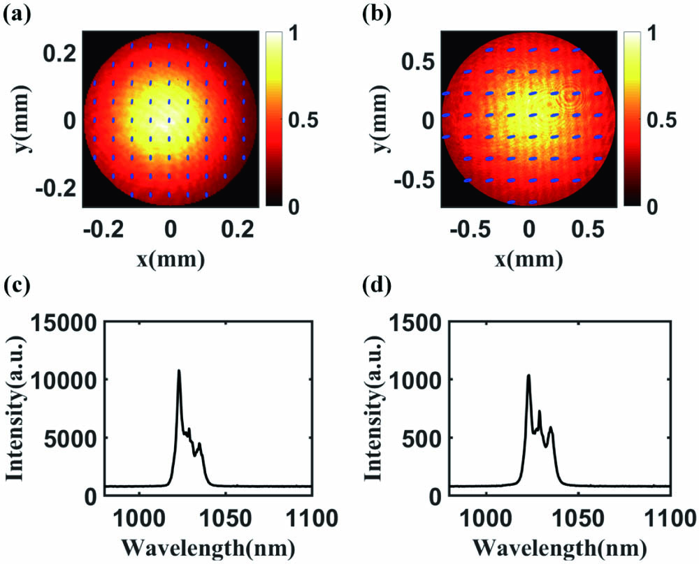
Fig. 2. (a) Intensity and polarization distributions of 1030 nm input laser in front of the vortex fiber (the ellipses represent the direction of polarization). (b) Intensity and polarization distributions of 1030 nm output laser behind the fiber tail. Spectra of 1030 nm laser (c) in front of and (d) behind the fiber.
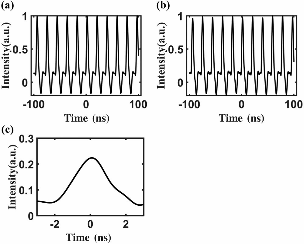
Fig. 3. Pulse sequences of 1030 nm laser (a) in front of and (b) behind the fiber. (c) Pulse width of excitation beam.
Then, we block the 1030 nm laser and adjust the polarization state of the incident 532 nm laser coupled to the vortex fiber to produce a ring-shaped output beam. The polarizer placed behind the vortex fiber is employed to qualitatively reveal the polarization pattern of the output beam, as shown in Fig. 4(a). The white arrow indicates the transmission axis of the polarizer. The intensity and polarization state distribution of the ring-shaped beam are quantitatively reconstructed by using the measured Stokes parameters, as shown in Fig. 4(b). The polarization of the output beam is axially symmetric and along the azimuthal direction, while the intensity distribution is in a donut shape. All of the above results prove that the output beam is the mode (i.e., azimuthally polarized beam), which can be used as the depletion beam for STED lithography.
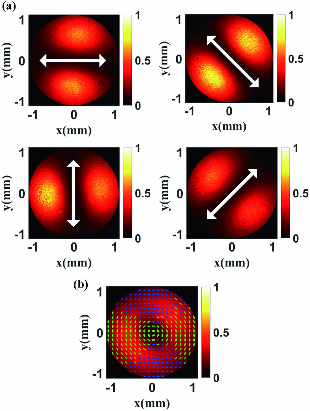
Fig. 4. (a) Output 532 nm laser after passing through a linear polarizer with different transmission axis orientations. (b) Intensity and polarization distributions of 532 nm laser behind the fiber tail.
Subsequently, the reconstructed field obtained by the Stokes parameters is employed to simulate the focused depletion beam PSF with the Richard–Wolf vectorial diffraction theory, as the following[27–
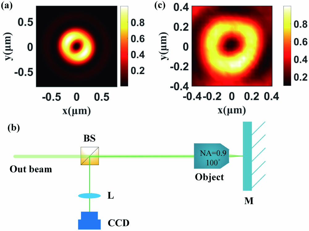
Fig. 5. (a) Simulated depletion beam PSF in the xy plane of the focal region. (b) Focus amplification system (BS, beam splitter; L, lens; M, mirror). (c) Experimentally measured focused depletion beam PSF.
An amplification system is built by using a high NA objective lens () and lens L to observe the tightly focused depletion beam PSF, as shown in Fig. 5(b). The mirror M is placed at the focal plane of the objective lens. The experimentally measured depletion beam PSF on the focal plane is shown in Fig. 5(c), from which the FWHM of the hollow center is estimated to be 226 nm by considering the amplification factor of 92. The experimental value is close to the simulated result. The discrepancy is mainly attributed to the limited precision of stages, the accuracy of the field measurement at the pupil plane, etc.
Similarly, the simulation results of the excitation beam PSF in the xy plane are shown in Fig. 6(a). The FWHMs of the excitation beam are found to be about 494 nm along the direction, and about 680 nm along the direction. The excitation beam PSF and depletion beam PSF overlapped in the xy plane; therefore, the effective beam intensity during the STED nanolithography process can be expressed as[31,32]
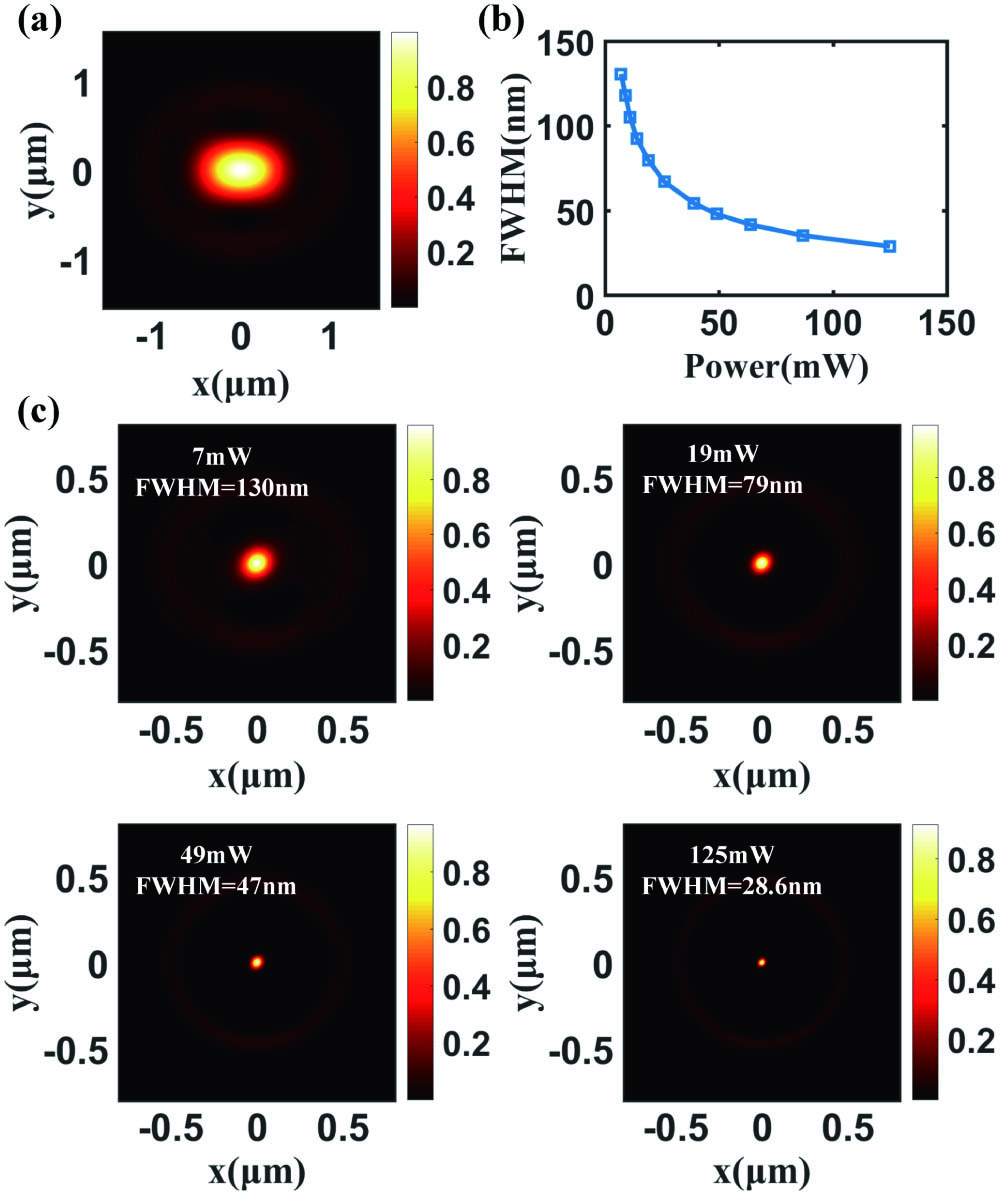
Fig. 6. (a) Simulated excitation beam PSF and (b) relationship between the FWHM of the effective beam and the power of the depletion beam in the xy plane of the focal region. (c) Intensity distribution of the effective beam in the xy plane of the focal region under different depletion beam powers.
4. Conclusion
A fiber-based source that is suitable for STED nanolithography is presented, which can generate an excitation beam and a donut-shaped depletion beam required by STED lithography. Such a fiber-based source maintains strictly coaxial alignment for the dual-beam setup. The experimental results indicate that the pulse width, spectrum, and repetition frequency remain unchanged when a pulsed beam with a central wavelength of 1030 nm passes through the system, which can serve as the excitation beam for STED lithography. The polarization of the excitation beam can be controlled to match with the polarization of the depletion beam, leading to improvement of the linewidth in direct laser writing. The mode of the 532 nm continuous laser is selected through the vortex fiber, and a donut-shaped azimuthally polarized beam is produced as the depletion beam of STED lithography. The measured Stokes parameters are carried out to quantitatively reveal the polarization and intensity distributions of the beams generated by the vortex fiber. Using the Richard–Wolf vector diffraction theory, the excitation beam and depletion beam PSFs in the focal region are simulated, and the effective beam in STED nanofabrication is analyzed. The effective FWHM decreases continuously as the power of the depletion beam increases, which provides the capability to break the diffraction limit. Compared with traditional STED lithography, fiber-based STED lithography is simpler, more stable, and easier to be integrated and miniaturized, which may be widely exploited in the field of micromachining.
[18] Z. Gan, Y. Cao, R. A. Evans, M. Gu. Three-dimensional deep sub-diffraction optical beam lithography with 9 nm feature size. Nat. Commun., 2013, 4: 2061.
[22] S. Ramachandran, P. Kristensen. Optical vortices in fiber. Nanophotonics, 2013, 2: 455.
Jian Chen, Guoliang Chen, Qiwen Zhan. Self-aligned fiber-based dual-beam source for STED nanolithography[J]. Chinese Optics Letters, 2021, 19(7): 072201.
