1 浙江大学极端光学技术与仪器全国重点实验室,浙江 杭州 310027
2 之江实验室,浙江 杭州 311121
双光子直写技术凭借其高精度、任意三维结构刻写、高成本效益、材料设计高自由度等特点,已被成功应用到多种微纳光学器件的刻写中。基于双光子直写的微纳光学器件应用不断拓展,对刻写分辨率和通量都提出了更高的需求。超分辨激光纳米直写和高通量激光直写技术使得双光子直写具有nm级精度与cm级尺寸的跨尺度加工能力,进一步拓展了基于双光子直写的微纳光学器件研究领域。本文首先对双光子直写原理进行概述,介绍本课题组在利用双光子直写技术制造衍射光学器件、光纤集成器件方面的研究进展;然后,介绍本课题组在使用超分辨激光直写技术制备纳米光子器件方面的拓展研究,并展示了高精度、高通量激光直写技术在大面积刻写微纳光学器件上的技术优势。
激光直写 双光子直写 微纳光学器件 纳米光刻 高通量刻写 光学学报
2023, 43(16): 1623013

Author Affiliations
Abstract
Optical antennas play an important role in optical field manipulation. Among them, nanoscale bowtie antennas have been extensively studied for its high confinement and enhancement. In this mini-review, we start with a brief introduction of bowtie antennas and underlying physics. Then we review the applications with respect to optically and electrically excited nanoscale bowtie antennas. Optically driven bowtie antennas enable a set of optical applications such as near-field imaging/trapping, nonlinear response, nanolithography, photon generation and detection. Finally, we put emphasis on the principle and applications of electrically driven bowtie antennas, an emerging method of generating ultrafast and broadband tunable nanosources. In a word, nanoscale bowtie antennas still have great potential research value to explore.Optical antennas play an important role in optical field manipulation. Among them, nanoscale bowtie antennas have been extensively studied for its high confinement and enhancement. In this mini-review, we start with a brief introduction of bowtie antennas and underlying physics. Then we review the applications with respect to optically and electrically excited nanoscale bowtie antennas. Optically driven bowtie antennas enable a set of optical applications such as near-field imaging/trapping, nonlinear response, nanolithography, photon generation and detection. Finally, we put emphasis on the principle and applications of electrically driven bowtie antennas, an emerging method of generating ultrafast and broadband tunable nanosources. In a word, nanoscale bowtie antennas still have great potential research value to explore.
bowtie antenna near-field imaging nanolithography nonlinear nanolaser inelastic tunneling Opto-Electronic Science
2022, 1(4): 210004
Author Affiliations
Abstract
1 National Engineering Research Center for High Efficiency Grinding, State Key Laboratory of Advanced Design and Manufacturing for Vehicle Body, College of Mechanical and Vehicle Engineering, Hunan University, Changsha 410082, People’s Republic of China
2 Advanced Design & Manufacturing Group for Micro/Nanophotonics, Jihua Laboratory, Foshan 528000, People’s Republic of China
Reliable fabrication of micro/nanostructures with sub-10 nm features is of great significance for advancing nanoscience and nanotechnology. While the capability of current complementary metal-oxide semiconductor (CMOS) chip manufacturing can produce structures on the sub-10 nm scale, many emerging applications, such as nano-optics, biosensing, and quantum devices, also require ultrasmall features down to single digital nanometers. In these emerging applications, CMOS-based manufacturing methods are currently not feasible or appropriate due to the considerations of usage cost, material compatibility, and exotic features. Therefore, several specific methods have been developed in the past decades for different applications. In this review, we attempt to give a systematic summary on sub-10 nm fabrication methods and their related applications. In the first and second parts, we give a brief introduction of the background of this research topic and explain why sub-10 nm fabrication is interesting from both scientific and technological perspectives. In the third part, we comprehensively summarize the fabrication methods and classify them into three main approaches, including lithographic, mechanics-enabled, and post-trimming processes. The fourth part discusses the applications of these processes in quantum devices, nano-optics, and high-performance sensing. Finally, a perspective is given to discuss the challenges and opportunities associated with this research topic.
extremely small manufacturing sub-10 nm fabrication nanolithography nanomanufacturing atomic-scale manufacturing International Journal of Extreme Manufacturing
2021, 3(3): 032002
Author Affiliations
Abstract
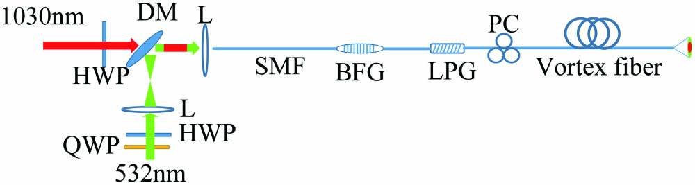
School of Optical-Electrical and Computer Engineering, University of Shanghai for Science and Technology, Shanghai 201800, China
A fiber-based source that can be exploited in a stimulated emission depletion (STED) inspired nanolithography setup is presented. Such a source maintains the excitation beam pulse, generates a ring-shaped depletion beam, and automatically realizes dual-beam coaxial alignment that is critical for two beam nanolithography. The mode conversion of the depletion beam is realized by using a customized vortex fiber, which converts the Gaussian beam into a donut-shaped azimuthally polarized beam. The pulse width and repetition frequency of the excitation beam remain unchanged, and its polarization states can be controlled. According to the simulated point spread function of each beam in the focal region, the full width at half-maximum of the effective spot size in STED nanofabrication could decrease to less than 28.6 nm.
nanolithography vortex fiber direct laser writing STED controlled fabrication Chinese Optics Letters
2021, 19(7): 072201

Author Affiliations
Abstract
1 Institute of Micro-Nano Photoelectron and Electromagnetic Technology Innovation, School of Electronics and Information Engineering, Hebei University of Technology, Tianjin 300401, China
2 Key Laboratory of Electronic Materials and Devices of Tianjin, Tianjin 300401, China
3 Semiconductor Lighting Technology Research and Development Center, Institute of Semiconductors, Chinese Academy of Sciences, Beijing 100083, China
A versatile nanosphere composite lithography (NSCL) combining both the advantages of multiple-exposure nanosphere lens lithography (MENSLL) and nanosphere template lithography (NSTL) is demonstrated. By well controlling the development, washing and the drying processes, the nanosphere monolayer can be well retained on the substrate after developing and washing. Thus the NSTL can be performed based on MENSLL to fabricate nanoring, nanocrescent and hierarchical multiple structures. The pattern size and the shape can be systemically tuned by shrinking nanospheres by using dry etching and adjusting the tilted angle. It is a natural nanopattern alignment process and possesses a great potential in the scope of nano-science due to its low cost, simplicity, and versatility for variuos nano-fabrications.
220.4241 Nanostructure fabrication 110.4235 Nanolithography Chinese Optics Letters
2017, 15(6): 062201
中国科学院光电技术研究所 微细加工光学技术国家重点实验室,成都 610209
本文将Bowtie 孔径结构与金属-介质-金属结构相结合,提出了一种新的局域表面等离子体共振纳米直写光刻结构,得益于金属-介质-金属结构中顶层透射Ag 对透射光的放大增强以及底层反射Ag 对透射光的反射补偿作用,聚焦光斑的尺寸得到压缩的同时深度得到了显著提高,理论仿真中当焦斑的FWHM 为28 nm 时,焦斑深度可以达到20 nm 以上,这相对于传统纳米直写光刻结构,将焦斑的深度提升了4 倍。随后,通过相关验证实验在光刻胶中获得了FWHM 为47 nm,曝光深度为25 nm 的焦斑图形,进一步证实了该结构在压缩焦斑尺寸以及提升焦斑深度上的显著优势。
局域表面等离子体共振 纳米直写光刻 Bowtie 孔径结构 金属-介质-金属结构 local surface plasmon resonance direct-writing nanolithography Bowtie aperture metal-insulator-metal
超透镜光刻技术是一种很有前景的纳米结构成像技术, 由于其具有可以克服衍射极限的能力, 直到2005年, 张翔和他的同事在365 nm紫外线波长下成功的对一排纳米线和刻在高分子膜上的四个字母“NANO”实现了超分辨成像, 分辨率高达1/6入射波长。通过传递矩阵方法优化出超透镜结构, 并通过选择适当的材料和设计在超透镜结构中的每个层的厚度以及合理的优化实验等方法制备一个新的超透镜结构, 利用这种超透镜结构实现了周期性纳米结构及孤立纳米结构的亚波长成像。实验结果表明, 对于周期性的纳米结构, 其图像分辨率达到100 nm, 而孤立结构的分辨率低于50 nm, 小于入射波长的1/7。
超透镜光刻 亚波长成像 周期性结构 孤立结构 superlens nanolithography subwavelength imaging periodic structures isolated structures 强激光与粒子束
2015, 27(2): 024131
1 中国科学院光电技术研究所 微细加工光学技术国家重点实验室,成都 610209
2 中国科学院研究生院,北京 100049
本文提出和研究了利用超分辨缩小成像平板超透镜,在i 线光源波长下实现纳米尺度光刻方法。为了在超分辨透镜像面位置获得高质量的光刻图形,采用超分辨透镜-光刻胶-反射银膜的结构方式,解决由于超透镜磁场偏振传输模式带来的成像光场畸变问题,大大提高了成像质量和光场对比度。采用掩模图形结构预补偿的方法,消除超分辨透镜的倍率畸变像差影响。基于有限元电磁计算方法,数值模拟结果验证了该方法在i 线光源波长下实现纳米尺度缩小成像光刻的可能性。在i 线(365 nm)光源波长下,得到约35 nm 线宽的高对比成像光场模拟结果,并分析了结构参数变化对成像光场带来的影响。
纳米光刻 超分辨成像 表面等离子体 超透镜 nanolithography sub-wavelength resolution imaging surface plasmons superlens
1 电子科技大学 物理电子学院, 成都 610054
2 中国科学院 光电技术研究所, 微细加工光学国家重点实验室, 成都 610209
介绍了一种利用激光干涉光刻技术得到特征图形,并通过离子束刻蚀将图形转移到铬层上,从而获得掩模的方法。针对掩模透光率以及对干涉图形对比度可能产生影响的两个参数分别进行了数值仿真,从而证明此方法的可行性和参数的优化选择。自搭干涉光刻实验系统,用257 nm的激光光源实现光刻,得到特征尺寸为100 nm的图形,再经过离子束刻蚀,最终得到周期200 nm、线宽100 nm的掩模。
激光干涉光刻 离子束刻蚀 纳米光刻 微纳结构制造 laser interference lithography ion beam etching nanolithography nanostructure fabrication
Author Affiliations
Abstract
State Key Laboratory of Precision Spectroscopy, Department of Physics, East China Normal University, Shanghai 200062, China
We report the fabrication of submicrometer pits array (SP-array) on 6H-SiC surface by the interference of two femtosecond laser beams. Formation mechanisms and optical absorption of SP-array are studied. The relative reflectivity and transmissivity of white light decrease to 10% of the values of SiC crystal, and the optical absorption is enhanced to 97%. The relative reflectivity and transmissivity of incident angles within the range of 20o~60o are kept below 25%. The enhancement mechanism of optical absorption of the SP-array is also discussed.
亚微米坑阵列 光吸收增强 双光束干涉 飞秒激光 320.7130 Ultrafast processes in condensed matter, including semiconductors 220.4241 Nanostructure fabrication 110.4235 Nanolithography Chinese Optics Letters
2010, 8(12): 1203


