Chinese Optics Letters, 2019, 17 (10): 100201, Published Online: Aug. 29, 2019  

Micro-fabrication and hermeticity measurement of alkali-atom vapor cells based on anodic bonding Download: 1321次

Author Affiliations
1 Science and Technology on Electronic Test and Measurement Laboratory, North University of China, Taiyuan 030051, China
2 Key Laboratory of Time and Frequency Primary Standards, National Time Service Center, Chinese Academy of Sciences, Xi’an 710600, China
Abstract
A vapor cell provides a well-controlled and stable inner atmosphere for atomic sensors, such as atomic gyroscopes, atomic magnetometers, and atomic clocks, and its hermeticity affects the stability and aging of atomic sensors. We present the micro-fabrication of a micro-electromechanical system wafer-level hermit vapor cell based on deep reactive ion etching and vacuum anodic-bonding technology. The anodic-bonding process with the voltage increasing in steps of 200 V had a critical influence on vapor cell hermeticity. Further, the silicon–glass bonding surface was experimentally investigated by a scanning electron microscope, which illustrated that there were no visual cracks and defects in the bonding surface. The leak rate was measured using a helium leak detector. The result shows that the vapor cells with different optical cavity lengths comply with the MIL-STD-883E standard (5 × 10 8 mbar·L/s). Moreover, D2 absorption spectroscopy was characterized via optical absorption. The bonding strength was determined to be 13 MPa, which further verified the quality of the vapor cells.

The interaction between light and atoms is an important component in many aspects of quantum optics research, including the Planck constant, Fano resonances[1,2], Bose–Einstein condensates[3], cold Rydberg atoms[4], and quantum sensing[5]. In modern society, an increasing amount of precision-metering information is needed for different variables, such as frequency, magnetic field, and gravity acceleration, which can be acquired from the interaction between light and atoms. The problems in traditional atomic sensors, especially with large volume, can be solved using micro-electromechanical systems (MEMS) technology[6,7]. MEMS technology has not only led to the development of the micro-manufacturing industry, but also meets the requirements of modern atomic sensors, such as small size, low consumption, light weight, and intelligent integration. Vapor cells, which are typical micro-reaction cavities providing a well-controlled and stable inner atmosphere for the interaction of atoms, are a key component for atomic sensors, including atomic gyroscopes, atomic magnetometers[8], and chip-scale atomic clocks[9,10].

The hermeticity of vapor cells and miniaturization of atomic clocks are two major problems that must be solved. Owing to the small size of a vapor cell, if a slight leak occurs, the alkali metal filled in the reactive cavity is easily oxidized, rendering the micro-sensor ineffective. Leak also causes a change in the composition of the buffer gas filled in the vapor cell, which deteriorates the long-term frequency stability of the atomic clock[11]. According to existing literature, several methods are used for wafer-level packing: anodic bonding[12,13], silicon fusion bonding[14,15], organic bond bonding[16], glass frit bonding[17], and solder bonding[18]. Anodic bonding has the merits of cost effectiveness and convenient reaction during the vapor cell fabrication process.

We present the micro-fabrication of an MEMS wafer-level hermit vapor cell based on vacuum anodic-bonding technology, in which the voltage is increased in steps of 200 V. Further, the bonding surface was experimentally investigated using a scanning electron microscope (SEM). The leak rate was measured using a helium leak detector. Analyses of D2 absorption spectroscopy, leak rate, and bonding strength verified the quality of the vapor cells.

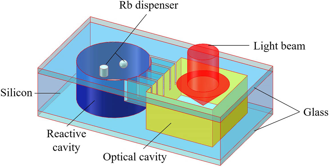
A microloop-gap resonator[19,20], the traditional optical microwave cavity, limits the requirement of a small volume in the vapor cell. Now, the coherent population trapping (CPT) principle is implemented in chip-scale atomic devices to achieve this goal. With the development of the MEMS technology, batch-fabrication of chip-scale atomic devices comes true. An MEMS wafer-level dual-cavity vapor cell with a glass–silicon–glass three-layer physical architecture is introduced, as shown in Fig. 1.

Fig. 1. Schematic of the dual-cavity vapor cell.

下载图片 查看所有图片

Reactions in a single-cavity vapor cell have limitations. The residue is not conducive to light passing through it, which will negatively affect the detection of the spectral line. However, such disturbances can be avoided in a dual-cavity vapor cell. What is more, a dual-cavity vapor cell provides different spaces for storing the alkali-metal dispenser (reactive cavity) and reacting for light and atoms (optical cavity). In the optical cavity, one pump beam generates a coherent, and another probe beam detects the optical signal. The two cavities are connected by micro-channels, which not only helps the alkali-metal atoms to diffuse from the reaction cavity to the optical cavity but also isolates substances from the reactive cavity to some extent.

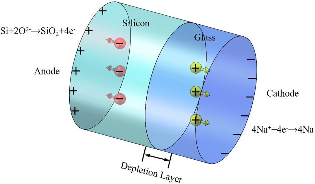
Anodic bonding is an encapsulation method commonly used for simple glass–silicon steps. The principle underlying the anodic bonding between silicon and glass is shown schematically in Fig. 2. When the temperature rises, the mobility of Na+ in the glass increases. When potential is applied, Na+ migrates toward the cathode, simultaneously forming a Na+ depletion layer at the interface of the Pyrex glass. At the same time, a positive image charge area is formed in the silicon wafer surface. The two areas attract each other, causing electrostatic force strength between the Pyrex glass and silicon to be on the order of 108V/m, resulting in a pressure of approximately 10–20 bar, which makes irreversible bonding at the silicon–glass contact interface possible. Moreover, the sealing between the silicon wafer and the Pyrex glass was no longer released after the voltage was removed. The anodic bonding is non-conductive, gas-tight, thermally stable, and chemically stable, and has high mechanical strength. Therefore, the two anodic-bonding materials should be selected with similar thermal-expansion coefficients. Otherwise, the bonding surface might crack or break due to the thermal stress generated during the anodic-bonding process[21].

Fig. 2. Schematic of the principle of anodic bonding.

下载图片 查看所有图片

In this experiment, we used a 4-in.-diameter, 1.5-mm-thick P-type <100> double-sided polished silicon wafer and two pieces of 4 in. 500-μm-thick BF33 glass plates that can be bonded to each other. The thermal-expansion coefficients of these materials are close to each other. For a high bonding strength, both the glass plates and silicon wafer must have high surface roughness and flatness, and they are thoroughly cleaned before use.

Fabrication of a vapor cell relies on the following technologies: silicon micromachining, rubidium dispenser manipulation, and packaging. The main four steps are fabricating silicon holes with deep reactive ion etching (DRIE) technology, placing the rubidium dispenser for producing natural abundance rubidium, sealing with the anodic-bonding technology, and alkali-metal reaction.

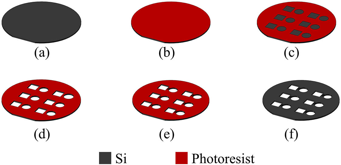
First, a double-sided polished silicon wafer is etched using photolithography with a mask and the DRIE technology, as shown in Fig. 3. The steps are as follows: (a) cleaning of the silicon wafer with the Radio Corporation of America standard to remove organic or inorganic contaminants and drying in the N2 stream; (b) spin coating with hexamethyldisilazane (HDMS) to ensure a strong adhesion of the photoresist to the substrate groups, and then spin coating with AZ 4620; (c) photolithography; (d) DRIE for forming cavities; (e) photolithography and DRIE for forming micro-channels; (f) cleaning of the silicon wafer. Cavities and micro-channels are fabricated using DRIE technology, providing a smooth interior wall; SEM images of two vapor cells are shown in Figs. 4(a) and 4(b). Figure 4(c) shows the simulated etching effect observed in a confocal microscope, and Figs. 4(d) and 4(e) show the etching depth during the etching process.
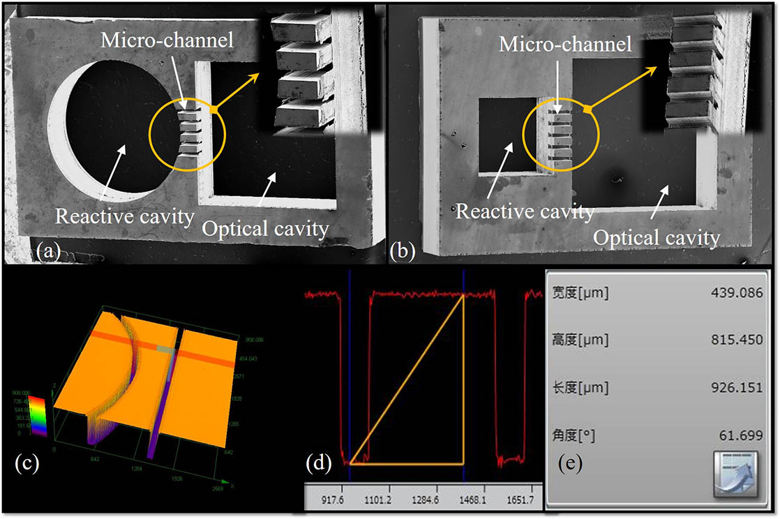
Fig. 3. Schematic of the DRIE of the silicon wafer of a vapor cell.

下载图片 查看所有图片

Fig. 4. (a) and (b) SEM images of a vapor cell with different shapes. (c) Schematic of the simulated etching effect. (d) and (e) Etching depth during the etching process.

下载图片 查看所有图片

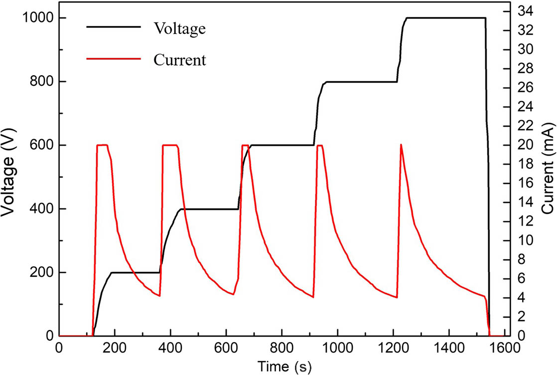
Second, the anodic-bonding process was performed using the EVG510 wafer bonding system (EV Group). The etched silicon wafer, after cleaning with acid and deionized water, and a BF33 glass plate of the same size are placed on a bonder chuck and clamped by three separation flags under a high-vacuum environment of 1×10⁵mbar, as shown in Figs. 5(a) and 5(b). Third, the two side heaters heat the silicon wafer and glass plate to the desired temperature, and the voltage is initially set to 0 V and increased in steps of 200 V from 0 V to 1000 V. The bonding contact pressure is 1500 N, and the anodic-bonding temperature is 500°C. The bonding curves of the process are shown in Fig. 6. The voltage was applied until the anodic-bonding current density decreased to 0.02mA/cm2. Fourth, thermal stresses caused by the heating process are released through a cooldown process because rapid temperature change may influence bulk materials, mostly glass. Fifth, when the temperature decreases to that of the ambient atmosphere, the alkali-metal compounds are carefully placed in the reactive cavity, as shown in Fig. 5(c). Placement of the rubidium dispenser can be accomplished using four methods: pipetting liquid alkali-atom drops (cesium or rubidium) under an anaerobic atmosphere[22,23], UV-light-induced decomposition of a deposited substance under a high-vacuum environment[24], laser ablation of alkali atoms encased in wax micro-packets[25], and evaporating alkali atoms into a cell by using a glass nozzle[26,27]. The above steps are repeated for the second anodic process, as shown in Figs. 5(d) and 5(e). A wafer-level hermetic MEMS vapor cell was obtained, as shown in Fig. 5(f).
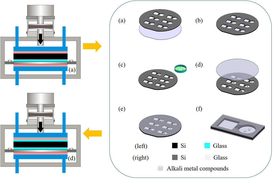
Fig. 5. Schematic of the anodic-bonding process. (a) and (b) First anodic bonding. (c) Filled alkali-metal compounds. (d) and (e) Second anodic bonding. (f) Completed vapor cell.

下载图片 查看所有图片

Fig. 6. Current–voltage curves during the anodic-bonding process.

下载图片 查看所有图片

The images of the etched silicon wafer and the bonded silicon wafer are shown in Fig. 7; vapor cells in two different samples were fabricated with a different size and shape. Then, those silicon wafers were cut into several separate chips with Disco DAD3220.
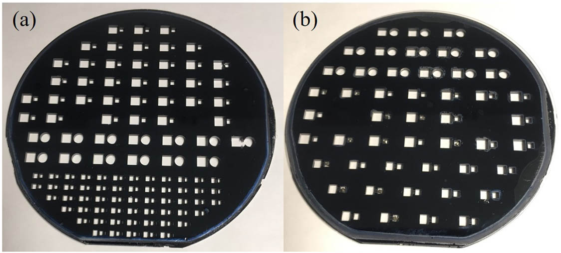
Fig. 7. (a) Image of the etched silicon wafer. (b) Image of the fabricated bonded silicon wafer.

下载图片 查看所有图片

Several double-cavity vapor cells have different lengths of optical cavities. Figure 8 shows the two chips without the high-power laser heating, and the rubidium dispenser is also visible. Then, the vapor cell is irradiated with a high-power Ti:sapphire laser with a wavelength of 852 nm to decompose the rubidium dispenser in the reactive cavities.

Fig. 8. Vapor cells of different optical cavity lengths compared with a dime: (a) 4 mm long and (b) 1 mm long.

下载图片 查看所有图片

We carried out the absorption spectroscopy experiment to verify the properties of the vapor cell. The light source is a vertical cavity surface emitting laser (VCSEL) tuned on the Rb D2 line at 780 nm. The linewidth is less than 300 kHz, and the diameter is 1 mm. The incident power is 320 μW. The laser was modulated with a 1 V, 10 Hz triangle wave. Then, the laser passed through an optical isolator, which can prevent optical feedback; then, a lens and a λ/4-wave plate were used to achieve circular polarization. The laser then passed through the heated vapor cell and triggered a photodiode to convert the beam into an electrical signal that can be observed through an oscilloscope. The rubidium D2 absorption spectroscopy test platform and spectra at different temperatures are shown in Fig. 9. The spectra exhibit four distinct peaks; the depth of each peak represents the relative abundance of an isotope in naturally occurring Rb, which consists of 72.17% Rb85 and 27.83% Rb87. Thus, the two signals with higher amplitudes correspond to the absorption of Rb85, whereas the outer two dips correspond to that of Rb87. The absorption peaks of Rb atom transitions can be observed, namely Rb87F=2F, Rb85F=3F, Rb85F=2F, Rb87F=1F[28,29].
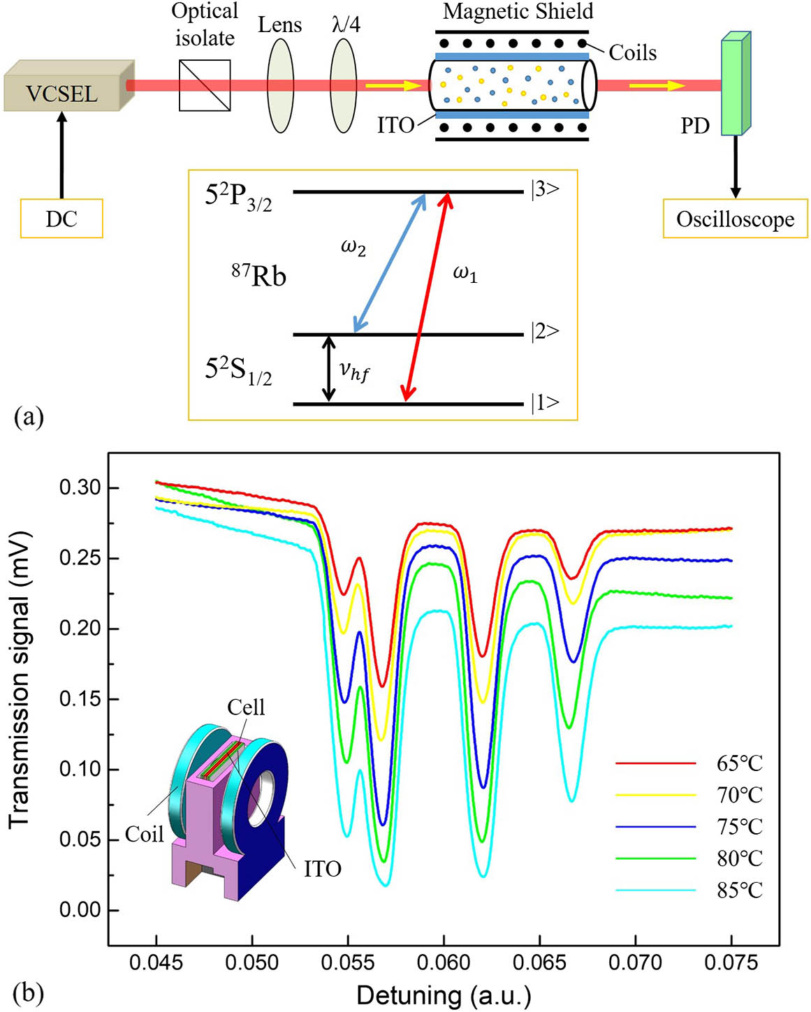
Fig. 9. (a) Test platform for D2 absorption spectroscopy. (b) D2 absorption spectra at different temperatures.

下载图片 查看所有图片

The relationship between the pressure P of a vapor cell and time t is given as follows[30]: dPdt=LPnormV(PextP),where Pnorm is the normal pressure, L is the leakage rate, V is the volume of the vapor cell cavity, and Pext is the external pressure. Based on Eq. (1), the pressure can be expressed as follows: P(t)=Pext(1eLtVPnorm),where the initial pressure is 103Pa. Therefore, the leakage rate can be expressed as follows[31,32]: L=V·ΔpΔt.

The hermeticity of the vapor cell affects the stability and aging of atomic sensors. According to the MIL-STD-883E, Method 1014.9 (1995), electronic device packaging always needs to measure the hermeticity. The process of helium fine inspection is as follows. (a) Adding helium pressure: place the vapor cell in a tank filled with helium gas. The tank is vacuumed in advance until it reaches a vacuum environment at 5 bar, and helium of purity of 99% is filled into the tank. After maintaining this state for approximately 4 h, the tank is slowly depressurized, and the vapor cells are extracted from the tank. (b) Purification: when the vapor cell is extracted from the tank, the surface-adsorbed helium is blown off with dry nitrogen. (c) Leak rate detection: put the vapor cell into the test container and connect the container to the helium leak detector. The container is vacuumed in advance, and the leak detector is checked for leak detection. By measuring the content of helium escaping from the package structure, the leak rate can be obtained. Figure 10 shows the result of the leak rate test by using an ALCATEL ASM 142 helium leak detector with the minimum helium leak rate detection of 1011mbar·L/s (the sensitivity of the helium leak detector). All of the vapor cells with different optical cavity lengths showed a leak rate of 5×10⁸mbar·L/s, which is in line with the MIL-STD-883E standard (5×10⁸mbar·L/s).
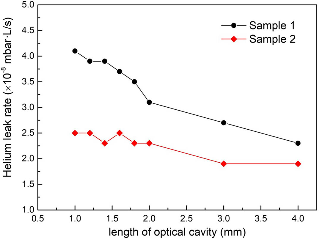
Fig. 10. Helium leak rate measurement of vapor cells with different optical cavity lengths.

下载图片 查看所有图片

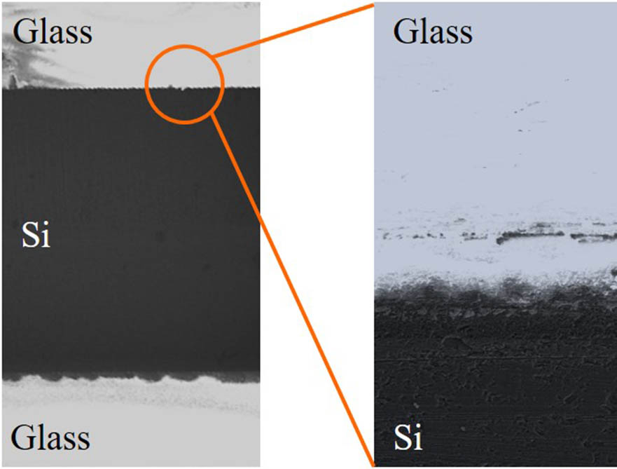
Furthermore, the silicon–glass adhesive layer was inspected by SEM to detect larger cracks. Figure 11 illustrates that there are no visual cracks and defects in the bonding surface. Subsequently, we tested the bonding strength, which is one of the most important indexes of vapor cells. The average tensile strength of the vapor cell obtained with an automatic bonding test machine was greater than 13 MPa.

Fig. 11. SEM images of the anodic-bonding surface.

下载图片 查看所有图片

The vapor cell plays an important role as a core component of atomic sensors. We have presented micro-fabrication of an MEMS wafer-level hermit vapor cell based on DRIE and vacuum anodic-bonding technology. Cavities and micro-channels were fabricated with DRIE technology, providing a smooth interior wall. The anodic-bonding process was performed with a maximum voltage of 1000 V and maximum current of 20 mA for vapor cell bonding, and the bonding had a critical influence on vapor cell hermeticity. In order to measure the bonding effect, the silicon–glass bonding surface was experimentally investigated by SEM, which illustrated that there were no visual cracks and defects in the bonding surface. The leak rate was measured using an ALCATEL ASM 142 helium leak detector. The result shows that the vapor cells with different optical cavity lengths comply with the MIL-STD-883E standard (5×10⁸mbar·L/s). Moreover, D2 absorption spectroscopy was characterized via optical absorption. The bonding strength was determined to be 13 MPa, which further verified the quality of the vapor cells. Based on analyses of the results, the presented vapor cells are deemed suitable for atomic sensors, such as atomic gyroscopes, atomic magnetometers, and atomic clocks. The dual-cavity vapor cell performed well; however, it makes miniaturization challenging because the volume of the dual-cavity is almost twice that of a single cavity. To solve this problem, we are investigating the encapsulation of single-cavity alkali-metal vapor cells, and the relevant research results will be reported in detail in another article.

References

[1] BrajeD., Physics3, 75 (2010).PHYSGM1943-2879

[2] MiroshnichenkoA. E.FlachS.KivsharY. S., Rev. Mod. Phys.82, 2257 (2010).RMPHAT0034-6861

[3] AnglinJ. R.WolfgangK., Nat. Photon.416, 211 (2002).NPAHBY1749-4885

[4] LimJ.LeeH.-g.AhnJ., J. Korean Phys. Soc.63, 867 (2013).KPSJAS0374-4884

[5] DegenC. L.ReinhardF.CappellaroP., Rev. Mod. Phys.89, 035002 (2017).RMPHAT0034-6861

[6] YangW.ConkeyD. B.WuB.YinD.HawkinsA. R.SchmidtH., Nat. Photon.1, 331 (2007).NPAHBY1749-4885

[7] GoreckiC., Procedia Eng.47, 898 (2012).

[8] FangJ.QinJ., Rev. Sci. Inst.83, 093902 (2012).

[9] KitchingJ., Appl. Phys. Rev.5, 031302 (2018).

[10] KnapkiewiczP., Micromachines (Basel)9, 405 (2018).

[11] AbdullahS.AffolderbachC.GruetF.MiletiG., Appl. Phys. Lett.106, 163505 (2015).APPLAB0003-6951

[12] ChenY.ShangJ.JiY., in 2013 IEEE 15th Electronics Packaging Technology Conference (EPTC 2013) (2013), p. 809.

[13] LvQ.HeL.XuJ., in International Conference on Electrical & Control Engineering (2011), p. 552.

[14] MalufN., Meas. Sci. Technol.13, 229 (2013).MSTCEP0957-0233

[15] SugaT.HosodaN., in IEEE International Workshop on Micro Electro Mechanical Systems (1995), p. 413.

[16] SpieringV. L.BerenschotJ. W.ElwenspoekM.FluitmanJ. H. J., J. Microelectromech. Syst.4, 151 (2002).JMIYET1057-7157

[17] TandeskeD., Sensor Rev.22, 265 (1990).SNRVDY0260-2288

[18] HuangW.-F.ShieJ.-S.LeeC.-K.GongS. C.PengC.-J., Proc. SPIE3893, 478 (1999).

[19] ViolettiM.MerliF.ZurcherJ.SkrivervikA. K.PellatonM.AffolderbachC.MiletiG., in IEEE SENSORS (2012), p. 1.

[20] ViolettiM.PellatonM.AffolderbachC.MerliF.ZurcherJ.-F.MiletiG.SkrivervikA. K., IEEE Sens. J.14, 3193 (2014).ISJEAZ1530-437X

[21] ZhangT.ZhangH.XuJ.LiuS.GanZ., Sens. Actuators A Phys.157, 168 (2010).

[22] LiewL.-A.KnappeS.MorelandJ.RobinsonH.HollbergL.KitchingJ., Appl. Phys. Lett.84, 2694 (2004).APPLAB0003-6951

[23] VecchioF.VenkatramanV.SheaH. R.MaederT.RyserP., Sens. Actuators A Phys.172, 330 (2011).

[24] LiewL.-A.MorelandJ.GerginovV., Appl. Phys. Lett.90, 114106 (2007).APPLAB0003-6951

[25] RadhakrishnanS.LalA., in International Conference on Solid-state Sensors (2005), p. 23.

[26] KnappeS.GerginovV.SchwindtP. D. D.ShahV.RobinsonH. G.HollbergL.KitchingJ., Opt. Lett.30, 2351 (2005).OPLEDP0146-9592

[27] BanK.HiraiY.TsujimotoK.TeraoA.MizutaniN.KobayashiT.TabataO., J. Vac. Sci. Technol. A34, 061601 (2016).JVTAD60734-2101

[28] ZhangX.YangG.DaiK.ChenY., Chin. Opt. Lett.15, 070201 (2017).CJOEE31671-7694

[29] WangA.MengZ.FengY., Chin. Opt. Lett.16, 050201 (2018).CJOEE31671-7694

[30] StraessleR.PellatonM.AffolderbachC.PétremandY.BriandD.MiletiG.de RooijN. F., J. Appl. Phys.113, 064501 (2013).JAPIAU0021-8979

[31] TaoY.MalsheA. P., Microelectron. Reliab.45, 559 (2005).MCRLAS0026-2714

[32] DellisA. T.ShahV.DonleyE. A.KnappeS.KitchingJ., Opt. Lett.41, 2775 (2016).OPLEDP0146-9592

Lu Zhang, Wendong Zhang, Shougang Zhang, Shubin Yan. Micro-fabrication and hermeticity measurement of alkali-atom vapor cells based on anodic bonding[J]. Chinese Optics Letters, 2019, 17(10): 100201.
引用该论文: TXT   |   EndNote

相关论文

加载中...

关于本站 Cookie 的使用提示

中国光学期刊网使用基于 cookie 的技术来更好地为您提供各项服务,点击此处了解我们的隐私策略。 如您需继续使用本网站,请您授权我们使用本地 cookie 来保存部分信息。
全站搜索
您最值得信赖的光电行业旗舰网络服务平台!