激光与光电子学进展, 2019, 56 (20): 202406, 网络出版: 2019-10-22
金属等离子体微纳结构对有机光电器件光场调控的研究  下载: 2233次特邀综述
Metallic Plasmonic Micro/Nano-Structures for Light-Field Manipulation in Organic Optoelectronic Devices
图 & 表
图 1. 等离子体微纳结构在OLEDs和OPVs中光学调控的基本原理。(a) SPP模式在金属/介质界面的电磁场分布[36];(b) SPP模式在金属/介质界面的衰减[36];(c) SPP和自由空间光子的色散关系[36];(d) SPP在周期性结构表面(周期为D)上的色散示意图[50];(e) OPVs中等离子体光散射效应示意图[55];(f) OPVs中近场增强效应示意图[55];(g) OPVs中SPP效应示意图[55]
Fig. 1. Basic principle of optical manipulation of plasma micro/nano-structures in OLEDs and OPVs. (a) Electromagnetic-field distribution of SPP mode at metal/dielectric material interface[36]; (b) decay of SPP mode at metal/dielectric material interface[36]; (c) dispersion relationship of SPP mode and free space photon[36]; (d) SPP dispersion on periodically structured surface (period D)[50]; (e) schematic of plasmonic light scattering in OPVs[55]; (f) schematic of near-filed enhanced effect in OPVs[55
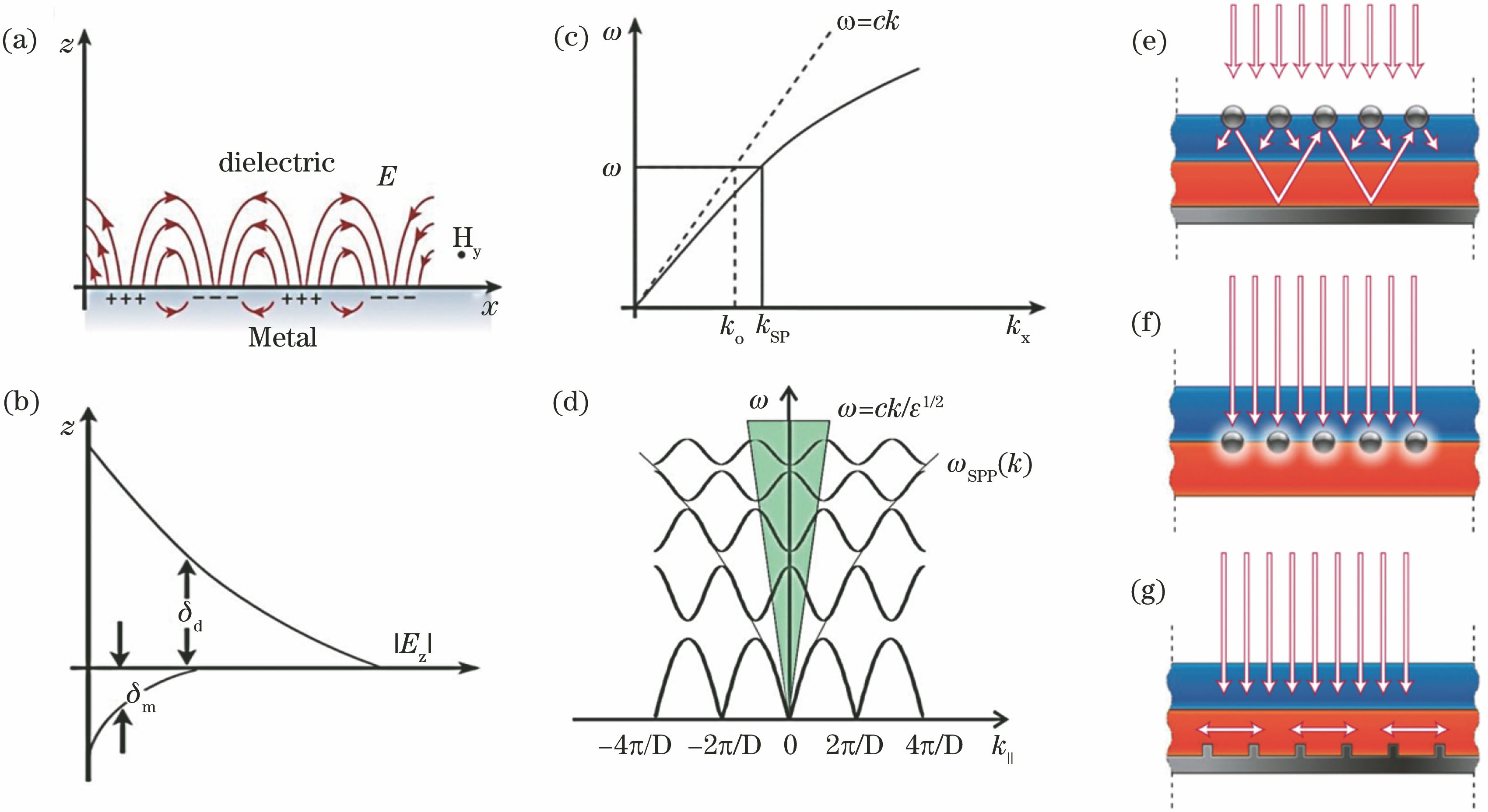
图 2. 激光辅助全息光刻技术。(a)基于激光干涉的全息光刻技术示意图[71];(b)多层次三维复合微纳结构的扫描式电子显微镜(SEM)照片[71]
Fig. 2. Laser-assisted holographic lithography. (a) Schematic of holographic lithography based on laser interference[71]; (b) scanning electron microscope (SEM) images of three-dimensional multiscale hierarchical micro/nano-structures[71]

图 3. 纳米压印技术。(a) Thermal NIL示意图[79];(b) UV-curable NIL示意图[79];(c)(d)利用UV-curable NIL制备的微纳结构的SEM照片[81-82];(e) Micro/nano-contact NIL示意图[79]
Fig. 3. Nanoimprint lithography. (a) Schematic of thermal NIL[79]; (b) schematic of UV-curable NIL[79]; (c)(d) SEM images of micro/nano-structures fabricated by UV-curable NIL[81-82]; (e) schematic of micro/nano-contact NIL[79]

图 4. 温度诱导制备微纳结构技术。(a)温度诱导制备微纳结构示意图[87];(b)基于不同热退火温度(85 ℃和105 ℃)诱导制备的波状微纳结构原子力显微镜(AFM)照片[87];(c)基于图案化弹性聚合物薄膜制备的有序微纳结构的SEM照片[90]
Fig. 4. Temperature-induced fabrication of micro/nano-structures. (a) Schematic of temperature-induced fabrication of micro/nano-structures[87]; (b) atomic force microscopy (AFM) images of temperature-induced micro-corrugations based on different annealing temperatures (85 ℃ and 105 ℃)[87]; (c) SEM images of temperature-induced complex ordered microstructures based on patterned elastomeric polymer surface[90]

图 5. 等离子微纳结构提取底发射OLEDs中的SPP和波导模式。(a)(b)基于单一周期微结构的OLEDs角度依赖EL光谱和器件内部场分布[104];(c)双周期等离子体光栅提取OLEDs中的双金属电极界面SPP损耗[111];(d)无金属电极的透明OLEDs的光取出示意图[113]
Fig. 5. Light extraction from SPP and waveguide modes in bottom-emitting OLEDs by micro/nano-structures. (a)(b) Angular dependent EL spectra and internal-field simulated distribution of magnetic field intensity in single-period micro/nano-structured OLEDs[104]; (c) extraction of SPP loss at bimetallic electrode interface in OLEDs by dual periodic gratings[111]; (d) schematic of light extraction from transparent OLEDs without metal electrodes[113]

图 6. 顶发射OLEDs的光提取。(a)(b)SPP模式与微腔模式交叉耦合提高厚金属电极的光取出效率示意图及色散关系[103];(c)顶发射白光OLEDs中TPP-MC杂化模式光提取示意图[140]
Fig. 6. Light extraction from top-emitting OLEDs. (a) (b) Schematic of cross-coupling of SPP and microcavity modes improving light-extraction efficiency of thick metal electrode and dispersion relation[103]; (c) schematic of TPP-MC hybrid-mode light extraction in white top-emitting OLEDs[140]

图 7. SPP模式提高OPVs光吸收。(a)基于不同周期一维光栅的OPVs的制备工艺、微结构AFM照片及吸收谱[161];(b) OPVs中周期性等离子体微纳结构的SEM照片[160];(c)双MEN结构提高OPVs中光吸收的示意图和MEN结构AFM照片[166]
Fig. 7. Light trapping in OPVs enhanced by SPP mode. (a) Fabrication process, AFM images of microstructures, and absorption spectra of OPVs based on one-dimensional grating with various of periods[161]; (b) SEM images of periodic micro/nano-structures in OPVs[160]; (c) schematic of light trapping in OPVs enhanced by in-cell and out-cell MEN microstructures and AFM images of MEN microstructures[166]

图 8. 不同形状金属Ag NPs提高OPVs光吸收。(a)和(b)、(d)和(e)不同形状Ag NPs的TEM照片[149];(c)和(f) Ag NPs尺寸统计分布[149]
Fig. 8. Light trapping in OPVs enhanced by Ag NPs with different metal shapes. (a)(b)、(d)(e) TEM images of different Ag NPs[149]; (c) (f) size-distribution histogram of Ag NPs[149]

图 9. 基于双等离子体纳米结构提高OPVs光吸收示意图[191]
Fig. 9. Schematic of light trapping in OPVs enhanced by dual plasmonic nanostructures[191]

图 10. 复合等离子体微纳结构提高OPVs光吸收。(a)复合等离子体微纳结构提高OPVs光吸收示意图[192];(b)复合等离子体微纳结构制备工艺流程图[192];(c)~(f)复合等离子体微纳结构的SEM照片(比例尺为1μm)[192]
Fig. 10. Light trapping in OPVs enhanced by composite plasmonic micro/nano-structure. (a) Schematic of composite plasma micro/nano-structure improving light trapping in OPVs[192]; (b) flowchart of fabrication of composite plasmonic micro/nano-structure[192]; (c)-(f) SEM images of composite plasmonic micro/nano-structure (scalebar is 1 μm)[192]

毕宴钢, 易方顺, 冯晶. 金属等离子体微纳结构对有机光电器件光场调控的研究[J]. 激光与光电子学进展, 2019, 56(20): 202406. Yangang Bi, Fangshun Yi, Jing Feng. Metallic Plasmonic Micro/Nano-Structures for Light-Field Manipulation in Organic Optoelectronic Devices[J]. Laser & Optoelectronics Progress, 2019, 56(20): 202406.


 PDF全文
PDF全文

