Chinese Optics Letters, 2018, 16 (1): 011404, Published Online: Jul. 17, 2018
Stress damage process of silicon wafer under millisecond laser irradiation  Download: 764次
Figures & Tables
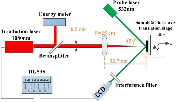
Fig. 2. Real-time images induced by different laser energy densities for (a) 19 and (b) 23 J / cm 2

Fig. 3. (a)–(d) Real-time images at different times. The laser energy density is 28 J / cm 2


Fig. 5. (Color online) (a) Temperature of spot center and (b) von Mises stresses along the X axis at 0.7, 1, 1.1, and 1.3 ms, respectively.


Fig. 7. (Color online) (a) Concentric circle and (b) shear stresses along it at 1.5 ms. S1, S2, and S3 represent the shear stress along (111)[110], (111)[101], and (111)[011], respectively.


Zhichao Jia, Tingzhong Zhang, Huazhong Zhu, Zewen Li, Zhonghua Shen, Jian Lu, Xiaowu Ni. Stress damage process of silicon wafer under millisecond laser irradiation[J]. Chinese Optics Letters, 2018, 16(1): 011404.


 PDF全文
PDF全文

