Photonics Research, 2020, 8 (11): 11001662, Published Online: Oct. 10, 2020
Hybrid nano-scale Au with ITO structure for a high-performance near-infrared silicon-based photodetector with ultralow dark current  Download: 669次
Figures & Tables
Fig. 1. Schematic process flow for the formation of ITO/Au/n-Si SPDs. (a) The PD areas were defined on an n-type Si substrate by ultraviolet lithography. (b) The patterned Si was sent to the electron beam evaporation chamber to grow Au film at room temperature. (c) 100 nm ITO was deposited on the Au film immediately by a double chamber magnetron sputtering system at room temperature under Ar / O 2
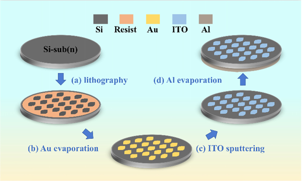
Fig. 2. (a) Cross-sectional scanning electron microscope (SEM) image of the 6AuSPD on the left, and a top view of the SEM images of the 0AuSPD (top) and 6AuSPD (down) in an area of 1 μm × 0.5 μm 5 μm × 5 μm

Fig. 3. (a) Room temperature J –V characteristics on a linear scale for the 0AuSPD and 6AuSPD under dark conditions; the inset map is the corresponding J –V data from − 0.2 J –V characteristics in semi-log for the 0AuSPD and 6AuSPD. (c) Temperature dependent J –V characteristics for the 6AuSPD. (d) In (J / T 2 T for the 0AuSPD and 6AuSPD. Experimental photocurrents and dark currents for the 0AuSPD and 6AuSPD with (e) a 1310 nm laser at a power of 1 mW and (f) a 1064 nm laser at a power of 2 mW.

Fig. 4. (a) Room temperature J –V characteristics in semi-log for AuSPDs under dark conditions; (b) ln (J / T 2 T for AuSPDs. (c) Photoresponse of AuSPDs measured at zero bias voltage from 1100 to 1700 nm. (d) Experimental photocurrents for AuSPDs with 1310 nm wavelength measured from − 1 V − 1 V
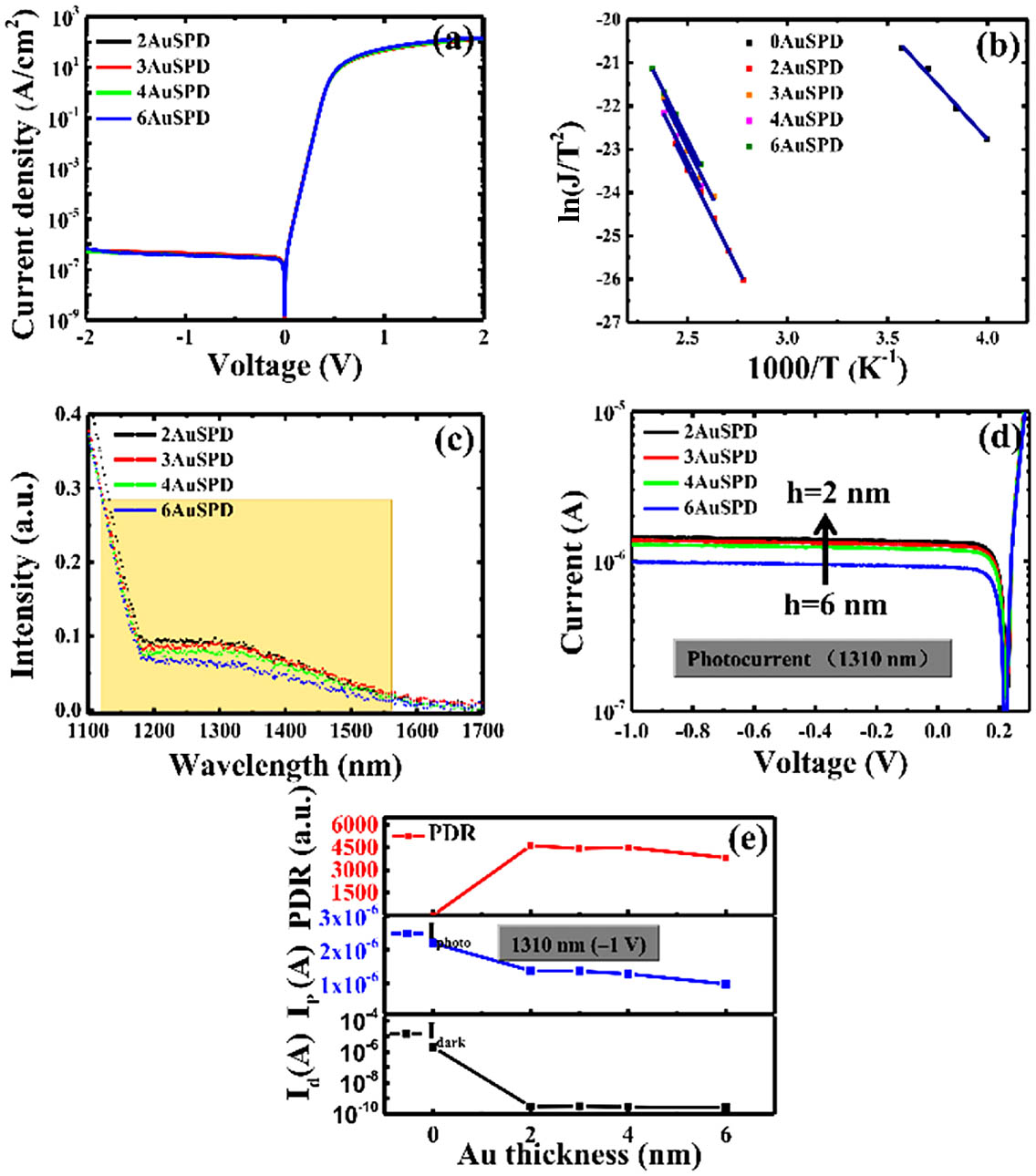
Fig. 5. (a) Samples were measured using a UV-VIS-NIR light spectrophotometer with light normal to the surface. (b) The corresponding photographs of these ITO/Au/glass films were taken under incandescent light with continuous spectrum showing considerable process uniformity in 2 cm × 2 cm


Fig. 7. (a) AFM images of the top electrodes in the 2AuSPD, 3AuSPD, 4AuSPD, and 6AuSPD with a scanned area of 5 μm × 5 μm. (b) Cross-sectional HRTEM images of the 2AuSPD, 3AuSPD, 4AuSPD, and 6AuSPD.

Fig. 8. Schematic diagram of the responsivity measurement for the 2AuSPD. A 1310 nm laser with a power of 2 mW was emitted through a single-mode fiber with an inner diameter of 9 μm onto the 2AuSPD arrays. The distance between the detector and the optical fiber outlet was about 2 mm and the numerical aperture (N A


Fig. 10. (a) Responsivity spectra with different biases of all AuSPDs. The values of the responsivities have been calibrated with a 1310 nm laser. (b) External quantum efficiency spectra with different biases of all AuSPDs.


Table1. Performance Comparison for Silicon-Based SPDs
|
Xinxin Li, Zhen Deng, Jun Li, Yangfeng Li, Linbao Guo, Yang Jiang, Ziguang Ma, Lu Wang, Chunhua Du, Ying Wang, Qingbo Meng, Haiqiang Jia, Wenxin Wang, Wuming Liu, Hong Chen. Hybrid nano-scale Au with ITO structure for a high-performance near-infrared silicon-based photodetector with ultralow dark current[J]. Photonics Research, 2020, 8(11): 11001662.


 PDF全文
PDF全文

