中国激光, 2021, 48 (2): 0202004, 网络出版: 2021-01-07
飞秒激光加工低维纳米材料及应用  下载: 2935次特邀综述
Femtosecond Laser Processing of Low-Dimensional Nanomaterials and Its Application
图 & 表
图 1. 时域整形飞秒激光双子脉冲烧蚀水环境中块体MoS2靶材的过程示意图[61]
Fig. 1. Schematic of temporally shaped femtosecond laser two sub-pulses ablating bulk MoS2 targets in water[61]
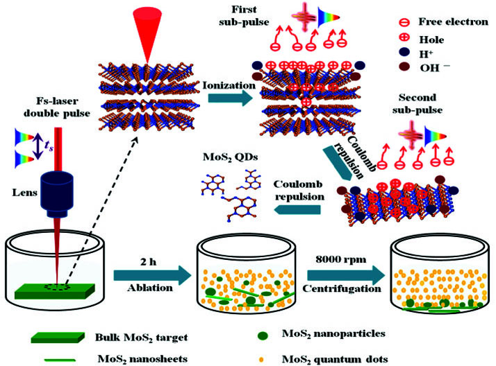
图 2. 前驱体材料作用的不同机制和选择性诱导化学反应路径示意图[62]。(a)辐射与相关分子能级发生共振时,分子才会对激光有响应;(b)弱场、短脉冲持续时间有助于克服共振约束;(c)分子振动能级和多光子激发产生足够的动态功率展宽;(d)最佳剪裁可以用来引导分子动力学选择反应通道
Fig. 2. Diagram of different mechanisms of precursor materials and selective induced chemical reaction paths[62]. (a) When the resonance occurs between the radiation and the related molecular level, molecular can response to laser; (b) constraints of resonance can be overcome in weak field and short pulse duration; (c) molecular vibrational energy level and multiphoton excitation produce enough dynamic power broadening; (d) best clipping can be used to g

图 3. a-MoSx的合成方法、结构和催化活性位点原理图[47]
Fig. 3. Schematic of preparation process, structure of a-MoSx, and catalytic active sites[47]

图 4. 制备的Ag纳米线和多种图案[65]。(a)不同能量下线宽和扫描速度的关系;(b)网格图案;(c)单词“NANO”;(d)四叶草图案
Fig. 4. Prepared Ag nanowires and varies of patterns[65]. (a) Relationship between line width and scanning speed at different laser powers; (b) mesh pattern; (c) letter ‘NANO’; (d) clover pattern

图 5. 在金膜表面加工获得的突破加工极限的纳米线结构示意图[67]。(a)空间光加工装置;(b)原始高斯光场分布;(c)整形后的光场分布
Fig. 5. Schematic of nanowire structure breaking through processing limit on Au film surface[67]. (a) Spatial optical processing setup; (b) original Gaussian optical field distribution; (c) optical field distribution after shaping

图 6. 基于MTA复合树脂的双光子聚合三维微纳结构[68]。(a)MTA复合树脂的制备示意图;(b)双光子聚合实验装置; (c)用来图案化Au电极的PET基底;(d)~(h)双光子聚合加工的三维微结构
Fig. 6. 3D micro/nano structure based on MTA composite resins obtained by two-photon polymerization (TPP) lithography[68]. (a) Schematic of preparation of MTA composite resins; (b) TPP experimental setup; (c) PET substrate for patterning Au electrodes; (d)--(h) 3D microstructures processed by TPP

图 7. 飞秒激光制备大面积“石墨烯花”微结构阵列并实现超疏水仿生表面的示意图[70]。(a)原始氧化石墨烯纳米片;(b)还原氧化石墨烯纳米片;(c)还原后的石墨烯纳米片滤膜;(d)在单脉冲、1.1 J/cm2通量下加工“石墨烯花”;(e)采用飞行打点模式加工“石墨烯花”阵列;(f)大面积均匀“石墨烯花”结构(右)和原始薄膜(左)的润湿性对比
Fig. 7. Schematic of large-area ‘graphene flower’ microarchitecture array obtained by femtosecond laser and realizing superhydrophobic bionic surface[70]. (a) Original graphene oxide nanosheet; (b) reduced graphene oxide nanosheets; (c) graphene nanoflake filter membrane after reduction; (d) prepared ‘graphene flower’ at a single pulse and fluence of 1.1 J/cm2; (e) ‘graphene flower’ arrays obtained by flight dot pattern; (f) wettability compar

图 8. FsLDW在非平面基底上还原和图案化GO薄膜[71]。(a)加工过程示意图;(b)弯折型微电路;(c)菲涅耳波带片;(d)二维码
Fig. 8. Reduced and patterned the GO films by FsLDW on nonplanar substrates[71]. (a) Schematic of processing; (b) bow-like microcircuit; (c) Fresnel zone plate; (d) quick response code

图 9. 时域整形飞秒激光诱导MoS2表面化学还原活性机理示意图[72]。(a)时域整形飞秒激光加工示意图;(b)~(d)MoS2周期性结构形貌和表面金颗粒形貌;(e)MoS2微/纳米碎片的原子尺度示意图
Fig. 9. Schematic of chemical reduction activity mechanism on MoS2 surface induced by temporally shaped femtosecond laser[72]. (a) Schematic of temporally shaped femtosecond laser processing; (b)--(d) MoS2 periodic structural morphology and surface gold particle morphology; (e) atomic-scale diagram of the MoS2 micro/nano debris

图 10. vdWHs的生长过程示意图[73]。(a)在位点处生长的金属相过渡金属硫化物;(b)激光加工示意图;(c)金属相-半导体相过渡金属硫化物异质结的三维原子结构
Fig. 10. Schematic of the vdWHs growth process[73]. (a) Metal phase transition metal sulfide grown at sites; (b) schematic of laser processing; (c) 3D atomic structure of metal-/semiconductor-TMDS heterojunctions

图 11. 基于“氧化还原梭”的光合成路径飞秒激光掺杂锐钛矿TiO2的原理图[75]
Fig. 11. Schematic of doping of anatase TiO2 by a femtosecond laser under the photosynthetic routes based on redox shuttle[75]

图 12. 分层多孔WO3纳米颗粒聚集物的示意图、形貌和光催化分解水性能[76]。(a)多孔WO3纳米颗粒聚集的分层结构示意图、相应的电荷转移和电解质渗透过程;(b)WO3纳米颗粒多孔团簇的光电化学活性;(c)形貌调控过程原理图; (d)多孔纳米颗粒团聚体电镜图(SEM)
Fig. 12. Schematic of the hierarchical porous WO3 nanoparticle aggregates, its morphology, and photoelectrochemical water splitting performance[76]. (a) Diagram of layered porous WO3 nanoparticle aggregation, corresponding charge transfer, and electrolyte permeation processes; (b) photoelectrochemical activity of porous WO3 nanoparticle aggregates; (c) schematic of morphology regulation process; (d) SEM image of porous nan

图 13. 硅-水界面等离子体增强还原AgN
Fig. 13. Plasma enhanced reduction of AgNO3 at silicon-water interface[80]. (a) Schematic of experimental mechanism; a1) Ag+ reduction at plasma-liquid interface during plasma expansion through hydrated electrons and free radicals produced by water decomposition; a2) formation of growth sites; (b) relationship between bubble diffusion distance and laser energy, and inset is the schematic of silver nanostructure on silicon surface; (c

图 14. 细胞存活检测法(MTT法)和存活细胞荧光图像的对比[82]。(a)不同细胞的存活率与MoS2纳米颗粒浓度的关系;(b)未处理的A549细胞的荧光显微图像;(c)MoS2纳米颗粒处理48 h后,A549细胞的荧光显微图像
Fig. 14. The cell viability assay method (MTT method)and the contrast of fluorescent images of living cells[82]. (a) Relationship between viability of different cells and concentration of MoS2 nanoparticles; (b) fluorescent microscopy image of untreated A549 cells; (c) fluorescent microscopy image of the A549 cells after MoS2 nanoparticles treating for 48 h

图 15. FsLDW诱导去氧化还原和图案化GO原理图、形貌和电学特性[83]。(a)GO微电路的制备过程示意图;(b)(c)梳齿状和曲线状微电路的SEM图;(d)(e)梳齿状和曲线状微电路的原子力显微镜(AFM)图;(f)飞秒激光还原前后GO薄膜轮廓示意图;(g)电学特性曲线
Fig. 15. Schematic of deoxygenation for reducing induced by FsLDW and patterning GO, morphology, and electrical property[83]. (a) Schematic of the preparation process of GO microcircuits; (b)(c) SEM images of comb-liked and curved microcircuits; (d)(e) AFM images of comb-liked and curved microcircuits; (f) schematic of GO thin film profile before and after femtosecond laser reduction; (g) electrical characteristic curve

图 16. 具有亚微米尺度分辨率的超级电容器结构示意图[84]。(a)~(e)实验过程示意图;(f)1T相MoS2滤膜的侧视SEM图;(g)拥有不同叉指的超级电容器的光学显微镜图像;(h)叉指处扫描电子显微镜(SEM) 图像和能量色散谱(EDS)分布;(i)微型超级电容器阵列的SEM图像;(j)高分辨率叉指的SEM图像
Fig. 16. Schematic of supercapacitor structure with submicron scale resolution[84]. (a)--(e) Schematic of experimental process; (f) cross-section SEM image of 1T MoS2 filter film; (g) optical microscope images of a supercapacitor with different fingers; (h) SEM images and EDS distribution of fingers; (i) SEM image of miniaturized supercapacitor arrays; (j) SEM image of finger with high resolution

图 17. 多孔碳微型超级电容器原理图、形貌和循环伏安(CV)特性响应[85]。(a)激光碳化法制备微型超级电容器的原理图;(b)贴在小瓶弯曲壁上的微型超级电容器照片;(c)靠近中心缝隙处的多孔碳片的SEM图像;(d)微型超级电容器对不同程度机械弯曲的CV响应,插图为实验中的弯曲模态
Fig. 17. Schematic of the miniaturized supercapacitor with porous carbon, its morphology, and CV responses[85]. (a) Schematic of laser carbonization method to fabricate miniaturized supercapacitor; (b) photo of a miniaturized supercapacitor attached to the curved wall of a vial; (c) SEM images of porous carbon sheets near the center crack; (d) CV response of miniaturized supercapacitors to different degrees of mechanical bending, and inset is experimental

田梦瑶, 左佩, 梁密生, 许晨阳, 原永玖, 张学强, 闫剑锋, 李欣. 飞秒激光加工低维纳米材料及应用[J]. 中国激光, 2021, 48(2): 0202004. Mengyao Tian, Pei Zuo, Misheng Liang, Chenyang Xu, Yongjiu Yuan, Xueqiang Zhang, Jianfeng Yan, Xin Li. Femtosecond Laser Processing of Low-Dimensional Nanomaterials and Its Application[J]. Chinese Journal of Lasers, 2021, 48(2): 0202004.


 PDF全文
PDF全文

