Due to the massive growth of the internet traffic, next-generation optical communication systems combining wavelength division multiplexing (WDM) and time division multiplexing (TDM) require multiple wavelength channels of short optical pulses[1]. Meanwhile, with the increasing demands in high-speed analog-to-digital converters (ADCs) in various signal processing applications, optical analog–digital conversion (OADC) has been proposed to break the sampling speed limitation of electronic ADCs. In some typical OADC schemes, multiwavelength sampling sources are indispensable[2,3]. Various multichannel sampling source generation approaches have been reported, including mode-locked fiber lasers[46" target="_self" style="display: inline;">–6], external cavity mode-locked lasers[7], photonic integrated multichannel mode-locked lasers[8,9], spectral slicing of LEDs[10], and super-continuum spectrum generation[11]. Compared to hybrid integrated array modules consisting of several discrete devices, monolithically integrated mode-locked laser arrays could potentially reduce the system costs by simplifying optical alignment and packaging processes. Mode-locked laser diodes (MLLDs) based on distributed Bragg reflectors (DBRs) could be used to generate high-frequency and short optical pulses, capable of realizing compact, cost-effective, wavelength-tunable, and mass-producible laser sources. It is suitable to be the fundamental building block for MLLDs in addition to the commonly used building blocks, such as semiconductor optical amplifiers (SOAs), multimode interference (MMI) couplers, and MMI reflectors (MIRs)[12]. Besides, due to its wavelength tunability, each channel can be used as a backup for other channels in WDM systems.
Recently, Hou et al. reported a and mode-locked DBR laser array monolithically integrated with a MMI combiner, SOA, and an electro-absorption modulator (EAM)[8,13,14]. In this structure, the active and passive sections used the same quantum well structure. The bandgap shift of the passive DBR section was realized by using rapid thermal annealing. The wavelength-tuning range of each mode-locked channel was only about 2 nm by tuning the DBR section current, which needs further improvement. The DBR array adopted surface gratings with four different periods that were prepared by electron-beam lithography. The surface grating requires a well-controlled deep etching process to guarantee the grating quality. A simple and easily accessible etching process will be preferred.
In 2016, we reported a monolithically integrated four-channel harmonically mode-locked semiconductor laser based on an arrayed waveguide grating (AWG)[9]. However, because the AWG was very long, the repetition rate of the pulse output was low. In this Letter, we demonstrate a four-channel 40 GHz DBR-MLLD array monolithically integrated with a MMI optical combiner. The DBR-MLLD adopts butt-joint regrowth (BJR) to optimize the active section and passive section, respectively. The gratings were fabricated using holographic lithography, which is more efficient and cheaper than electron-beam lithography. The DBR-MLLD can realize short pulses with a pulse width of 2.98 ps and wavelength tuning range of 8.4 nm.
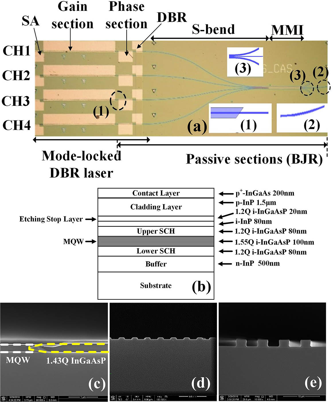
Figure 1(a) shows the microscope picture of the DBR-MLLD array. The DBR-MLLD has a total length of 1090 μm, corresponding to a fundamental mode-locking frequency of 40 GHz. It consists of a DBR section (70 μm), a phase section (150 μm), a gain section (730 μm), and a 50-μm-long saturable absorber (SA). The ratio between the SA section and the gain section was chosen to be 7% to obtain an optimum working condition according to our previous work[15]. Meanwhile, there is one 30-μm-long electrical isolation slot between each pair of these four sections, and the coupling efficiency of the DBR was about 40 cm−1. The passive sections contain a phase section, a DBR section, an S-bend, and a 4 × 1 MMI (322 μm). The butt-joint technique was adopted to integrate the active and passive sections. A 45° butt-joint angle was formed in the active–passive interface to reduce the interface reflection, as shown in the inset in Fig. 1(a)[(1)]. The output port of the MMI was prepared with a tilt angle of 7°. To minimize the influence of the reflection from the end of the MMI section to the MLLD, two bend waveguides were introduced to dissipate the residue optical field that was not collected by the output waveguide, as shown in the insets in Fig. 1(a)[(2) and (3)], respectively[16]. Figure 1(b) shows the epitaxial structure of the DBR-MLLD. The epitaxial structure was grown on an InP substrate via metal–organic chemical vapor deposition (MOCVD) to the upper separate confinement heterostructure (SCH). Then, the passive sections were defined by reactive-ion etching (RIE), and it was etched to down to the InP buffer layer. The core layer of the passive sections had a bandgap wavelength of 1.43 μm (1.43 Q). Figure 1(c) shows the scanning electron microscope (SEM) picture of the BJR, where the left side is the multiple quantum well (MQW) section, and the right side is the 1.43 Q passive section. The grating was fabricated using holographic exposure and RIE, with a period of 237 nm, as shown in Fig. 1(d). The 80 nm i-InP, 20 nm 1.2 Q i-InGaAsP (etch stop layer), 1.5 μm p-InP, and 200 nm p+ contact InGaAsP were grown successively on top of the active and passive regions. A 3-μm-wide ridge waveguide was defined by RIE terminated at the etch stop layer, followed by wet etch terminated at the upper SCH. Figure 1(e) shows the access waveguides of the MMI.
Fig. 1. (a) Optical microscope picture of the DBR-MLLD laser array, (b) the epitaxial laser wafer structure, (c) scanning electron microscope (SEM) picture of the BJR, (d) gratings, and (e) the access waveguides of the MMI.
下载图片 查看所有图片
In the measurement, the temperature of the DBR-MLLD was maintained at 25°C by a thermoelectric cooler. The four channels of the MLLD were designed to work simultaneously. Due to the lack of probes, we measured the four channels separately. Figure 2(a) shows the light-current (L-I) characteristics of the four separate laser channels (CH1–CH4) measured at the MMIs’ output port. The L-I characteristics of the four channels measured at the SAs’ output are shown in Fig. 2(b). The threshold current with an unbiased SA section was about 74 mA, and the current deviation within the four channels was less than 6 mA. The output power deviation was less than 1 dB when the gain section was biased at 300 mA. Figure 2(c) shows the typical L-I characteristics of a laser channel at different SA biased voltages. Due to the quantum-confined Stark effect (QCSE), an increase of the SA reverse voltage raises the threshold current and reduces the slope efficiency[17]. The output pulses of the laser were coupled into the fiber and an optical isolator. A 9:1 fiber coupler was used to split the output into two paths.
Fig. 2. (a) DBR-MLLD L-I characteristics of the four channels from the MMI output, (b) the DBR-MLLD L-I characteristics of the four channels from the SA output, (c) the L-I characteristics of a typical channel with different bias voltages of the SA. (d)–(f) Measured results when , with the other section floating: (d) optical spectral width fit, (e) RF spectral width fit, and (f) autocorrelation trace fit.
下载图片 查看所有图片
The 10% part was sent to an optical spectrum analyzer (Advantest Q8384) to measure the optical spectrum, and the 90% part was used to measure the RF spectrum (Agilent PXA-N9030 A) and the autocorrelation trace (APE-150). Figure 2(d) shows the typical optical spectra of the DBR-MLLD, with the full width at half-maximum (FWHM) of 1.1 nm. Figure 2(e) shows the beating RF signal of the mode-locked laser modes. The −3 dB linewidth of the beating signal was 348 kHz. The laser pulse has a pulse width of 2.98 ps using a sech2 fit of the autocorrelation trace, as shown in Fig. 2(f), and the corresponding time-bandwidth product (TBP) is 0.39.
To characterize the wavelength tunability of the DBR-MLLD, and were changed to tune the center wavelength. The optical spectra, RF spectra, and autocorrelation traces of a typical channel in various lasing states are shown in Figs. 3(a1)–3(d1), 3(a2)–3(d2), and 3(a3)–3(d3), respectively. At working conditions of , [0 V, 193 mA, 9.0 mA], [−0.4 V, 173 mA, 3.3 mA], [0 V, 163 mA, 0 mA], the peak wavelength of the MLLD reached 1575, 1577.9, 1580.5, and 1583.4 nm, with the signal to noise ratio (SNR) of 41.9, 43.5, 30.9, and 34.8 dB respectively, as shown in Fig. 3. The wavelength tuning range reached 8.4 nm. The pulse widths were 4.2 ps, 3.6 ps, 1.9 ps, and 2.5 ps, respectively. Figure 4 shows the dependence of the peak wavelength (), pulse repetition frequency (Fr), pulse width, and TBP on the DBR tuning current when was fixed at 164.1 and 182.6 mA, respectively. For all tested , the peak wavelength showed blue-shift when was increased from 0 to 10 mA [see Fig. 4(a)]. Figure 4(b) shows the pulse repetition frequency, where a tuning range of about 200 MHz was obtained when was varied from 0 to 10 mA. The pulse width (Gaussian fit) and TBP are shown in Figs. 4(c) and 4(d), respectively.
Fig. 4. Typical channel characteristics: (a) emission peak wavelength (), (b) pulse repetition frequency (Fr), (c) pulse width, and (d) TBP versus for , 182.6 mA while all other sections are left floating.
下载图片 查看所有图片
Fig. 3. Typical channel lasing characteristics of the DBR-MLLD biased at different conditions. (a1)–(d1) measured optical spectra, (a2)–(d2) measured RF power spectra, (a3)–(d3) measured autocorrelation traces. (a) , , ; (b) , , ; (c) , , ; (d) , , .
下载图片 查看所有图片
Figure 5 shows the optical spectra, RF spectra, and autocorrelation traces of the four channels at appropriate biased currents. The peak wavelength of the four channels is located at 1584.2, 1580.8, 1578.3, and 1575.2 nm, respectively, as shown in Fig. 5(a). The corresponding RF signals have peak frequencies at 39.896, 39.937, 40.001, and 39.890 GHz, respectively, with a channel frequency difference less than 110 MHz, as shown in Fig. 5(b). Such a small frequency difference enables a hybrid mode-locking possibility. The autocorrelation trace of the four channels is shown in Fig. 5(c), and the pulse widths are 1.8, 2.5, 3.2, and 6.6 ps, respectively.
Fig. 5. (a) Superposition of the four-channel optical spectra, (d) superposition of the four-channel RF spectra, and (c) the autocorrelation trace of the four channels.
下载图片 查看所有图片
In conclusion, we designed and fabricated a DBR-MLLD array and achieved simultaneous lasing of the four channels. The shortest pulse width of 1.8 ps, wavelength tuning range of 8.4 nm, and inter-channel frequency difference less than 110 MHz were demonstrated using the DBR-MLLD. The DBR-MLLD could be an alternative short pulse source of OADC and optical communication systems.
Huan Wang, Lu Guo, Wu Zhao, Guangcan Chen, Dan Lu, Lingjuan Zhao. 4 × 40 GHz mode-locked laser diode array monolithically integrated with an MMI combiner[J]. Chinese Optics Letters, 2019, 17(11): 111402.


