超薄氮化镓基LED悬空薄膜的制备及表征  下载: 557次
1 Introduction
Gallium nitride (GaN) materials have excellent optical, electrical, mechanical and piezoelectric properties[1-2]. By changing the content of In, Ga and Al, the energy gap of the material can be regulated, and the luminescent devices in ultraviolet, visible and near-infrared bands can be prepared[3-5]. High-quality silicon-based gallium nitride wafers are becoming more mature by introducing the buffer layers to release the residual stress caused by lattice mismatch and thermal expansion inconsistency. The advantages of silicon-based material, such as low cost, large wafer size, good heat dissipation and easy peeling, combined with the excellent photoelectric performance of gallium nitride material, have laid a material foundation for the research of wafer-level silicon-based gallium nitride micro-nano LED devices and related MOMES[6-8]. At present, the main bottleneck limiting the application of GaN-based LED device with silicon substrate is the adverse effect of silicon substrate and GaN epitaxial layer on the photoelectric performance of LED devices[9-11]. Due to the lattice mismatch and thermal expansion inconsistency between silicon substrate and GaN epitaxial layer, the wafer has a high internal stress[12-14]. The realization of silicon-based GaN MOMES requires the preparation of GaN-based freestanding membrane, so it is a key research difficulty to solve the problem of stress release in a large-area GaN-based freestanding membrane.
The current Chinese and international research efforts on improving the performance of silicon-based GaN LED device mainly involve the following technical route: imaging the silicon substrate, adding a Bragg reflector to the space between silicon substrate and epitaxial layer, and transferring the LED device to copper substrate. From the perspective of material growth, the research team led by Professor Takashi Egawa from the Nagoya University of Technology in Japan used the Metal-Organic Chemical Vapor Deposition (MOCVD) technology to prepare the Distributed Bragg Reflector (DBR) structure between silicon substrate and GaN epitaxial layer in order to reduce the absorption of LED-emitted light by the silicon substrate[15-16]. This team also used the Selective Laser Lift-Off (SLO) technique to remove the silicon substrate below the light-emitting zone of LED device, and transferred the LED device to the space above the copper substrate through bonding so as to improve the photoelectric performance of the device[17]. The research team led by Professor ZHANG Bai-jun from Sun Yat-Sen University transferred the LED device fabricated on a silicon-based gallium nitride wafer to an electroplated copper substrate. After the substrate transfer, part of the stress in the GaN epitaxial layer is released, which is beneficial to reduce the quantum-limited Stark effect of LED device[18-19]. The team led by Professor XIONG Chuan-bing from Nanchang University transferred the GaN-based LED membrane with silicon substrate to a substrate with a flexible bonding layer, and obtained an LED device not bound to substrate[20]. They also characterized and analyzed the stress changes before and after the transfer of LED device and its photoluminescence spectra by using high-resolution X-ray diffractometer and spectrometer. However, the above research work has not involved the preparation and optical property analysis of a large-area GaN-based LED freestanding membrane with sub-micron thickness that can be applied to MOMES system.
In this paper, the techniques of silicon substrate lift-off and freestanding GaN membrane backside thinning were developed based on silicon-based gallium nitride wafer. By using the backside process, a large-area ultrathin GaN-based LED freestanding membrane of sub-micron thickness was prepared. The morphology and optical properties of the LED freestanding membrane were tested and characterized. The optical properties of LED freestanding membrane are closely related to its thickness and deformation. The research on the large-area GaN-based LED freestanding membrane with sub-micron thickness also provides a possibility for the integration of GaN-based LED device with dynamic and adjustable MOMES system.
2 Fabrication and morphological characterization of ultra-thin GaN-based LED freestanding membrane
In this paper, the ultra-thin GaN-based LED freestanding membrane based on GaN-on-silicon wafer was prepared by combining the backside process with photolithography, Deep Reactive Ion Etching (DRIE) and Fast Atom Beam (FAB) etching. Silicon-based gallium nitride wafers were produced by Suzhou Lattice Power using the MOCVD technology. The substrate of a silicon-based gallium nitride wafer is made of thinned 200 μm thick silicon material. From bottom to top, the layered structure of GaN epitaxial layer is composed of a 900 nm Al(Ga)N buffer layer, a 400 nm undoped GaN layer, a 3.2 μm n-type GaN layer, a 250 nm InGaN/GaN multilayer quantum well layer (active luminous layer), and a 220 nm p-type GaN layer. The total thickness of GaN epitaxial layer is 4.9 nm. Both the silicon substrate and the GaN epitaxial layer will adversely affect the optical performance of LED device. The silicon substrate will absorb the outgoing light generated by the active layer of LED device, so will the epitaxial layer. This will cause the reflection dissipation of the outgoing light in the epitaxial layer.
The backside process for preparing the ultra-thin GaN-based LED freestanding membrane is shown in
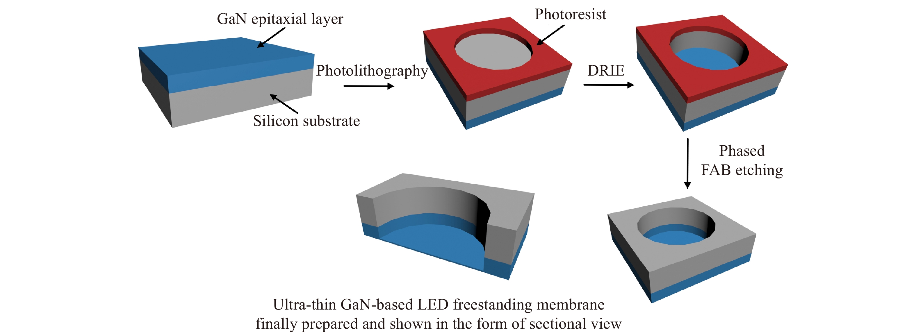
图 1. 超薄氮化镓基LED悬空薄膜工艺流程图
Fig. 1. Fabrication process of ultra-thin GaN-based LED freestanding membrane
In order to study the deformation and stress release rules of the LED freestanding membranes in different sizes, we designed four types of round LED freestanding membranes with different diameters (100, 200, 400 and 800 μm). The membrane areas range from 31 400 μm2 to 2 009 600 μm2, covering the possible sizes of GaN-based MOMES system. The
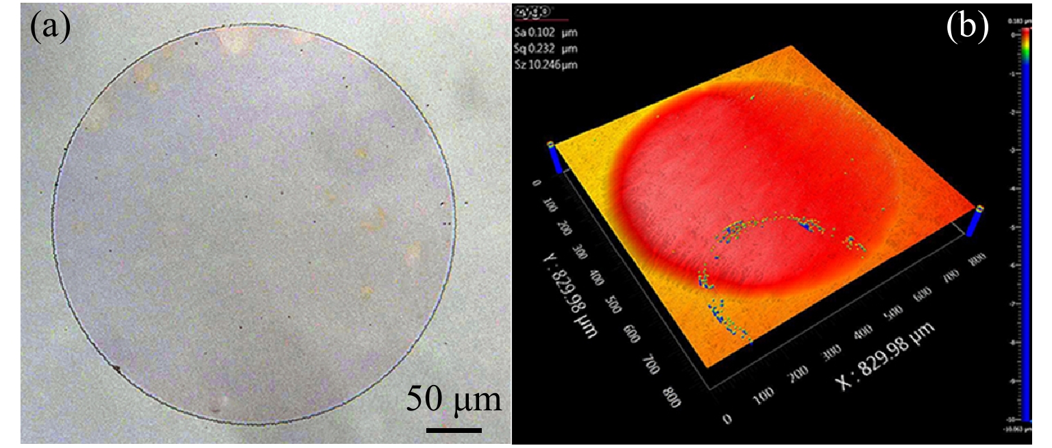
图 2. 剥离硅衬底的直径为800 μm的LED悬空薄膜的 (a)正面光镜图及(b)白光干涉仪获得的悬空薄膜三维变形图
Fig. 2. LED freestanding membrane with 800 μm diameter after removing silicon substrate. (a) Top-view optical microscope image, (b) 3D deformation image obtained by white light interferometer
The LED freestanding membranes with different diameters and thicknesses prepared by backside process have different surface deformations, as can be seen in

图 3. 具有不同直径的LED悬空薄膜的变形情况。 (a)掏空硅衬底,(b)背后减薄一次,(c)背后减薄两次
Fig. 3. Deformations of LED freestanding membranes with different diameters. (a) Removing silicon substrate, (b) thinning the backside once, (c) thinning the backside twice
3 Optical characterization of ultrathin GaN-based LED freestanding membrane
In the above text, we studied and analyzed the morphological characteristics of ultrathin GaN-based LED freestanding membrane. In this section, we will study its optical characteristics and analyze how to improve its optical performance. We will also use a reflectance spectrometer to test the membranes that have been thinned on the backside to different thicknesses. With the wavelength range of 450~850 nm, the reflectance spectrometer tests the reflectance spectrum of the membranes from the normal incident direction. The reflected light on the membrane surface and that on the bottom interface interferes with each other. The resulting reflectance spectrum can be used to characterize the membrane thickness and the number of modes. The thicker the membrane, the more the harmonic peaks (the number of modes) caused by interference.
For the silicon-based GaN sample without backside processing, the total thickness of its GaN epitaxial layer, including silicon substrate, is 4.9 μm. In the
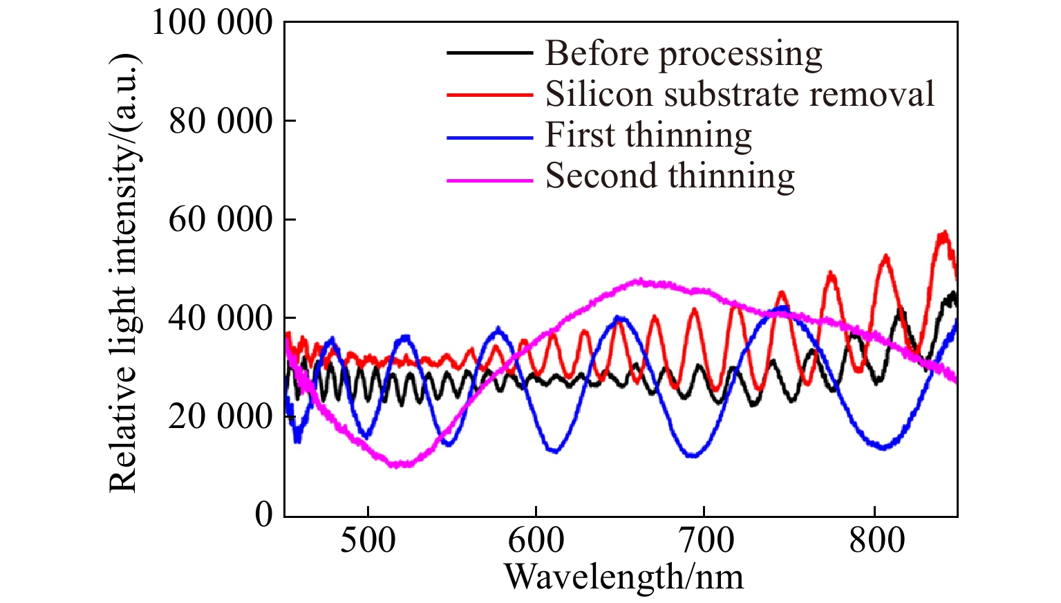
图 4. 具有不同厚度LED悬空薄膜的反射谱
Fig. 4. Reflectance spectra of LED freestanding membranes with different thicknesses
After that, a He-Ne laser with a wavelength of 325 nm is used to excite the active layer of quantum well of LED freestanding membrane to generate the emergent light, which is then tested for photoluminescence and for spectrum measurement by a wide-spectrum spectrometer. Due to the large lattice mismatch and thermal mismatch between silicon substrate and GaN epitaxial layer, a thick Al(Ga)N buffer layer is introduced into the GaN epitaxial layer to compensate for the lattice mismatch and thermal expansion. There is a large internal stress between silicon substrate and GaN epitaxial layer. Under the condition of photoluminescence excitation from the membrane front, we have studied the photoluminescence spectrum where the internal stress between GaN epitaxial layer and silicon substrate is released through the backside process. After the release of internal stress, the quantum well band structure of LED freestanding membrane will change, resulting in the corresponding change of its photoluminescence spectrum. As can be seen from
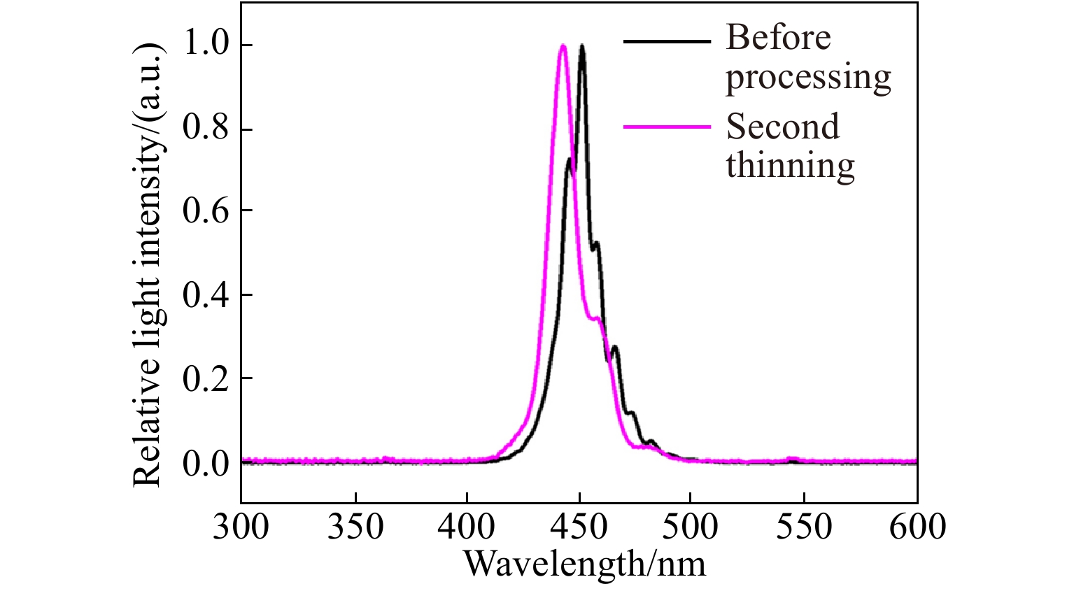
图 5. 正面激发下不同厚度LED悬空薄膜的光致发光谱
Fig. 5. Photoluminescence spectra of LED freestanding membranes with different thicknesses under front excitation
As shown in
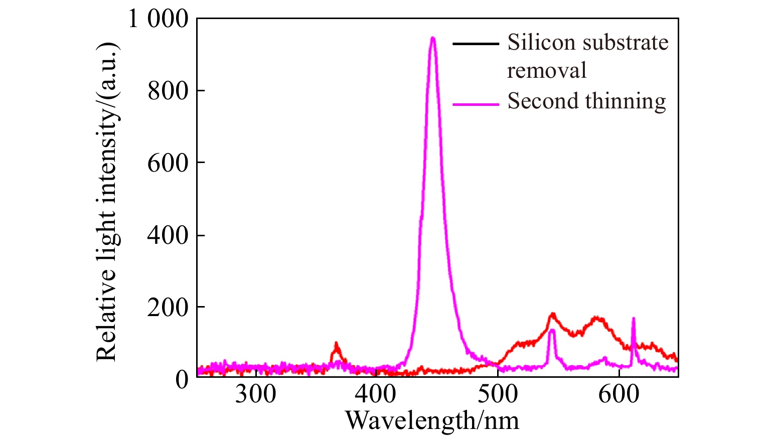
图 6. 背面激发下不同厚度LED悬空薄膜的光致发光谱
Fig. 6. Photoluminescence spectra of LED freestanding membranes with different thicknesses under backside excitation
4 Conclusion
In this paper, an ultra-thin GaN-based LED freestanding membrane based on the backside process has been obtained by using a silicon-based gallium nitride wafer. By peeling off the silicon substrate through deep reaction ion etching and thinning the backside of GaN epitaxial layer through FAB etching, the epitaxial layer was thinned from 4.9 μm to about 600 nm. We studied the deformation and optical characteristics of LED freestanding membranes with different thicknesses and sizes. The overall membrane deformation increases with the membrane diameter and decreases with the membrane thickness. The membrane as a whole presents the arch deformation with a bulging center and a smooth edge. After the backside thinning, the deformation of the membrane with a diameter of 800 μm decreases from 400 nm to 100 nm. The reflectance spectrum test shows that the freestanding membrane with a thickness of 4.9 μm has 27 interference modes, while the membrane with a thickness of 600 nm has only 1 interference mode. The front photoluminescence test shows that the release of internal stress generated by the backside process causes the change of quantum well band structure. Compared with unprocessed silicon-based gallium nitride wafer, the spectral peak of the 600 nm thick membrane has a blue shift of 8.2 nm. In the photoluminescence test on the backside, obvious outgoing light can also be detected from the ultra-thin LED freestanding membrane with most of the GaN epitaxial layer removed. With small overall deformation, a large round LED freestanding membrane of submicron thickness can be applied to the MOMES system requiring precise operation and control. Fewer interference modes of the membrane can help derive more easily the outgoing light generated by the active layer of LED device. This membrane provides a new way for the application of GaN-based LED device in the field of MOMES.
1 引 言
氮化镓材料拥有优异的光学、电学、机械和压电性能[1-2]。通过改变In、Ga、Al的含量,可以调控材料的禁带宽度,制备紫外、可见光及近红外波段的发光器件[3-5]。通过引入缓冲层来消除晶格失配以及热膨胀不一致引起的残余应力,生产高质量的硅衬底氮化镓晶圆技术日益成熟。利用硅作为衬底原料具有成本低廉、晶圆尺寸大、散热性能好、衬底易于剥离等优点,结合氮化镓材料优异的光电性能,为进行晶圆级硅基氮化镓微纳LED器件及相关的光微机电系统的研究工作奠定了材料基础[6-8]。目前限制硅衬底氮化镓基LED器件应用的主要瓶颈是硅衬底和氮化镓外延层对LED器件光电性能的不利影响[9-11]。此外,由于硅衬底和氮化镓外延层之间存在晶格失配及热膨胀不一致等问题,晶圆内部存在较大的内应力[12-14]。而硅基氮化镓光微机电系统的实现需要制备氮化镓基悬空薄膜器件,而大面积氮化镓基悬空薄膜内应力的释放问题也是研究难点。
目前,国内外关于改善硅基氮化镓LED器件性能的研究工作,主要涉及下述技术:图形化硅衬底、在硅衬底和外延层间添加布拉格反射镜、将LED器件转移至铜衬底。日本名古屋工业大学Takashi Egawa教授研究小组从材料生长的角度,利用金属有机化合物化学气相沉积(MOCVD)技术在硅衬底和氮化镓外延层之间制备分布式布拉格反射镜(DBR)结构,减少硅衬底对LED出射光的吸收[15-16]。该小组也利用选择性激光剥离(SLO)去除LED器件发光区下方的硅衬底,并利用键合工艺将LED器件转移至铜衬底上方,以提升LED器件的光电性能[17]。中山大学张佰君教授研究小组将制备在硅基氮化镓晶圆上的LED器件转移至电镀铜衬底上。在衬底转移后,氮化镓外延层中的部分应力得到释放,有利于减小LED器件的量子限制斯塔克效应[18-19]。南昌大学熊传兵教授小组将硅衬底氮化镓基LED薄膜转移至带有柔性黏结层的衬底上,获得了不受衬底束缚的LED器件[20],并分别利用高分辨率X射线衍射仪和光谱仪,表征分析了LED器件转移前后的应力变化及LED器件的光致发光光谱。以上研究工作都尚未涉及能够应用于光微机电系统的大面积亚微米厚度氮化镓基LED悬空薄膜的制备和光学特性分析。
本文基于硅基氮化镓晶圆,开发了硅衬底剥离及悬空氮化镓薄膜背后减薄工艺,利用背后工艺制备了大面积亚微米厚度的超薄氮化镓基LED悬空薄膜,并对LED悬空薄膜进行了形貌测试及光学性能表征。LED悬空薄膜的光学特性和薄膜厚度及变形情况密切相关。大面积亚微米厚度氮化镓基LED悬空薄膜的研究也为氮化镓基LED器件与可动可调控的光微机电系统的集成提供了可能性。
2 超薄氮化镓基LED悬空薄膜的制备及形貌表征
本文的研究工作结合光刻工艺、深反应离子刻蚀(DRIE)技术和快速原子束刻蚀(FAB)技术,利用背后工艺制备基于硅基氮化镓晶圆的超薄氮化镓基LED悬空薄膜器件。硅基氮化镓晶圆由苏州晶能光电公司利用MOCVD技术生产。硅基氮化镓晶圆的衬底是经过减薄的厚度为200 μm的硅材料,氮化镓外延层从下至上依次为900 nm厚的Al(Ga)N缓冲层、400 nm厚的无掺杂GaN层、3.2 μm厚的n型GaN层、250 nm厚的InGaN/GaN多层量子阱层(为有源发光层)、220 nm的p型GaN。氮化镓外延层的总厚度为4.9 μm,硅衬底和氮化镓外延层都会对LED器件的光学性能造成不利影响。硅衬底会吸收LED器件有源层产生的出射光,外延层也会吸收出射光,并造成出射光在外延层内的反射耗散。
制备超薄氮化镓基LED悬空薄膜器件背后工艺的过程如
为研究制备具有不同尺寸的LED悬空薄膜的变形和应力释放规律,本文设计了4种具有不同直径的圆形LED悬空薄膜,其直径分别为100、200、400和800 μm,薄膜面积从31 400 μm2至2 009 600 μm2,涵盖了氮化镓基光微机电系统可能包括的典型尺寸。
利用背后工艺制备的不同直径、不同厚度的LED悬空薄膜的表面变形程度如
3 超薄氮化镓基LED悬空薄膜的光学特性表征
在上文中,研究分析了超薄氮化镓基LED悬空薄膜器件的形貌特征。本节将深入研究超薄氮化镓基LED悬空薄膜器件的光学特性,以此为基础,分析其光学性能的提升。利用反射谱测试设备对经过多次背后减薄,厚度不同的氮化镓基LED悬空薄膜进行测试。反射谱测试设备所使用的光源波长范围为450~850 nm,选取正入射方向测试悬空薄膜的反射光谱。薄膜表面的反射光和薄膜与底部界面的反射光相互干渉,形成的反射谱可以表征薄膜的厚度和模式数。薄膜厚度越厚,干涉现象产生的谐振峰(即模式数)越多。
未经过背后加工的硅衬底氮化镓样品,其氮化镓外延层总厚度为4.9 μm,带有硅衬底,
之后利用波长为325 nm的He-Ne激光器激发LED悬空薄膜的量子阱有源层产生出射光,进行光致发光测试,并使用宽谱光谱仪测试出射光的光谱。由于硅衬底与氮化镓外延层之间存在较大的晶格失配和热失配,氮化镓外延层中引入了较厚的Al(Ga)N缓冲层来弥补晶格失配及热膨胀造成的影响。在从LED悬空薄膜正面进行光致发光激发的情况下,研究经过背后工艺释放了氮化镓外延层与硅衬底间内部应力的光致发光光谱。LED悬空薄膜器件的量子阱能带结构在内部应力释放后会发生改变,其光致发光光谱也会发生相应变化。由
从背后对LED悬空薄膜器件进行光致发光测试,如
4 结 论
本文利用硅基氮化镓晶圆制备了基于背后工艺的超薄氮化镓基LED悬空薄膜器件。利用深反应离子刻蚀技术剥离硅衬底,并利用快速原子束刻蚀技术从背后减薄氮化镓外延层,将厚度为4.9 μm的氮化镓外延层减薄至600 nm左右。本文研究了具有不同厚度、不同尺寸的LED悬空薄膜的变形程度和光学特性。结果显示:LED悬空薄膜整体变形随薄膜直径的增大而增大,随着薄膜厚度的减小而减小,且整体呈现中央凸起边缘平滑的拱形变形。经过背后减薄处理后,直径为800 μm的LED悬空薄膜变形从400 nm降低至100 nm。反射谱测试表明厚度为4.9 μm的悬空薄膜的干涉模式数为27,厚度为600 nm的悬空薄膜的干涉模式数降低为1。正面光致发光测试结果表明背后工艺产生的内部应力释放会造成量子阱能带结构变化,相较于未加工的硅基氮化镓晶圆,厚度为600 nm的LED悬空薄膜的出射光峰值波长出现了8.2 nm的蓝移。从背后进行光致发光测试发现,移除了大部分氮化镓外延层的超薄LED悬空薄膜也可以测试到明显的出射光。大尺寸亚微米厚的圆形LED悬空薄膜整体变形小,可应用于需要精确动作操控的光微机电系统,薄膜干涉模式数少,可以更容易地导出LED有源层产生的出射光,为氮化镓基LED器件在光微机电系统领域的应用开辟了新的途径。
[1] PEARTON S J, ZOLPER J C, SHUL R J. GaN: processing, defects, and devices[J]. Journal of Applied Physics, 1999, 86(1): 1-78.
[3] NAKAMURA S, PEATRON S, FASOL G. The Blue Laser Diode: the Complete Sty[M]. 2nd ed. Berlin: Springer, 2000.
[15] ISHIKAWA H, ASANO K, ZHANG B. Improved characteristics of GaN-based light-emitting diodes by distributed Bragg reflector grown on Si[J]. Physica Status Solidi (A), 2004, 201(12): 2653-2657.
Article Outline
李欣, 沙源清, 蒋成伟, 王永进. 超薄氮化镓基LED悬空薄膜的制备及表征[J]. 中国光学, 2020, 13(4): 873. Xin LI, Yuan-qing SHA, Cheng-wei JIANG, Yong-jin WANG. Fabrication and characterization of ultra-thin GaN-based LED freestanding membrane[J]. Chinese Optics, 2020, 13(4): 873.
