InP基近红外单光子雪崩光电探测器阵列  下载: 3147次封面文章
Indium Phosphide-Based Near-Infrared Single Photon Avalanche Photodiode Detector Arrays
1 中国科学院半导体研究所集成光电子学国家重点实验室, 北京 100086
2 中国科学院大学材料科学与光电技术学院, 北京 100049
图 & 表
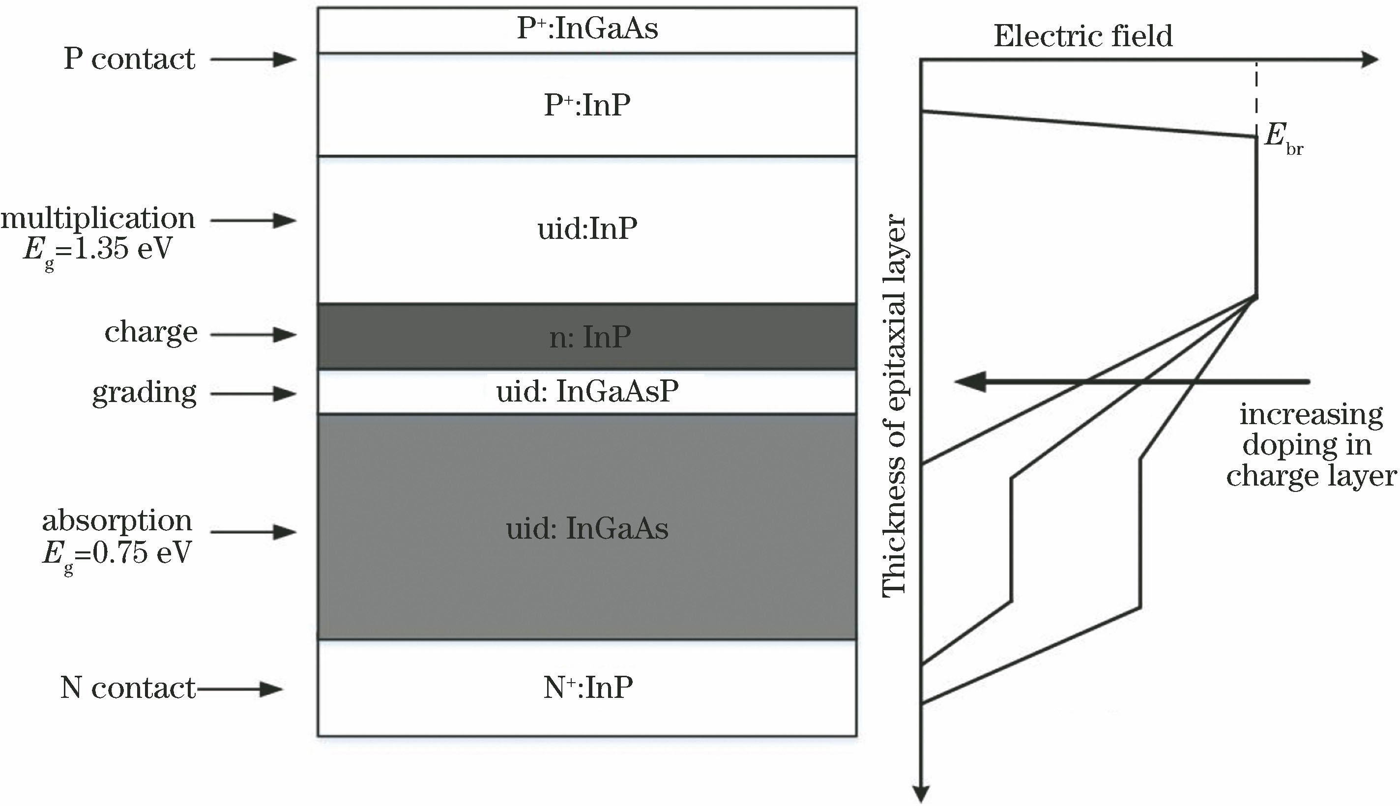
图 1. SAGCM层叠结构和内部电场分布
Fig. 1. SAGCM laminated structure and internal electric-field distribution
下载图片 查看原文
图 2. 参数关系。(a) PDE在不同温度下与过偏压的关系[15];(b)固定PDE时,不同倍增层厚度下DCR与PDE的关系[16]
Fig. 2. Parameter relationships. (a) Relationship between PDE and over-bias at different temperatures[15]; (b) relationship between DCR and PDE for devices with different thicknesses of multiplication layers and fixed PDE[16]
下载图片 查看原文
图 3. 参数关系。(a)不同倍增层厚度器件的DCR与过偏压的关系;(b)过偏压为4 V时,不同倍增层厚度器件的DCR与温度的关系[15]
Fig. 3. Parameter relationships. (a) Relationship between DCR and over-bias for devices with different thicknesses of multiplication layers; (b) relationship between DCR and temperature for devices with different thicknesses of multiplication layers at 4 V over-bias[15]
下载图片 查看原文
图 4. InGaAsP/InP SPAD的器件平台设计和阵列图像。(a) MIT设计的InGaAsP/InP SPAD外延层和台面结构示意图;(b)单个像元的显微照片;(c) 4×4阵列的显微照片[24]
Fig. 4. Device platform design and array image of InGaAsP/InP SPAD. (a) Schematic of epitaxial layer and mesa structure of InGaAsP/InP SPAD designed by MIT; (b) micrograph of individual pixel; (c) micrograph of 4×4 detector array[24]
下载图片 查看原文
图 5. MIT制备的APD/CMOS。(a) 32×32 APD/CMOS阵列桥接后的显微照片;(b)高倍镜下APD/CMOS阵列中单个像元的显微照片[26]
Fig. 5. APD/CMOS prepared by MIT. (a) Micrograph of bridged 32×32 APD/CMOS array; (b) micrograph of individual pixel in APD/CMOS array at high magnification[26]
下载图片 查看原文
图 6. GM-APD的相关参数和横截面示意图。(a) GM-APD的PDE和串扰与过偏压的关系;(b)与MLA结合的InP GM-APD阵列的横截面示意图[33]
Fig. 6. Related parameters and cross-sectional schematic of GM-APD. (a) PDE and crosstalk as functions of over-bias of GM-APD; (b) cross-sectional schematic of InP GM-APD array combined with MLA[33]
下载图片 查看原文
图 7. InP GM-APD焦平面阵列结构示意图。(a) InGaAs(P)/InP GM-APD结构;(b)倒接焊GM-APD焦平面阵列
Fig. 7. Schematic of focal plane array structure of InP GM-APD. (a) Structure of InGaAs(P)/InP GM-APD; (b) reverse welding GM-APD focal plane array
下载图片 查看原文
图 8. 1×16 InGaAs/InP SPAD线阵[38]
Fig. 8. 1×16 InGaAs/InP SPAD line array[38]
下载图片 查看原文
图 9. 两个像元之间的光路简图。(a)没有金属沟槽;(b)有金属沟槽[38]
Fig. 9. Schematic of optical path between two pixels. (a) Without metal trenches; (b) with metal trenches[38]
下载图片 查看原文
图 10. InGaAs/InP雪崩光电二极管。(a)结构示意图;(b) 8×8阵列照片[39]
Fig. 10. InGaAs/InP avalanche photodiode. (a) Schematic of structure; (b) photograph of 8×8 array[39]
下载图片 查看原文
表 1台面型InGaAsP/InP SPAD在不同条件下的性能参数
Table1. Performance parameters of mesa-type InGaAsP/InP SPAD under different conditions
| Multiplication zone thickness /μm | Over bias /V | Operating temperature /K | PDE /% | DCR /(109 Hz·cm-2) |
|---|
| 1.4 | 5 | 280 | 53 | 22 | | 1.4 | 5 | 240 | 56 | 1.3 | | 2.0 | 10 | 240 | >70 | 1.3 |
|
查看原文
表 2Verghese等[31]在2007年发表的阵列像元实验结果
Table2. Experimental results of array pixel published by Verghese et al.[31] in 2007
| Absorption zone material | Operating temperature /K | Detection wavelength /μm | PDE /% | DCR /kHz | Dead time /μs |
|---|
| InGaAsP | 298 | 1.06 | 50 | <20 | 1 | | InGaAs | 240 | 1.55 | 45 | <20 | 6 |
|
查看原文
表 3PLI最新研制的InP GM-APD焦平面阵列参数
Table3. Parameters of focal plane array of InP GM-APD developed by PLI
| Array scale | 32×32[36] | 32×128[36] | 32×32[18] |
|---|
| Detectionwavelength /μm | 1.06 | 1.06 | 1.55 | | Operatingtemperature /K | 253 | 248 | 248 | | Average DCR /kHz | 14 | 3.7 | 17.9 | | Average PDE /% | 39 | 34 | 19.7 | | PDE error /% | 6 | 9 | - |
|
查看原文
表 4PDE为20%,工作温度为233 K时,器件在不同尺寸下的DCR和后脉冲概率统计分布
Table4. DCR and after-pulsing probability statistically distributed at different sizes when PDE is 20% and operating temperature is 233 K
| Devicediameter | 16 μm | 25 μm | 40 μm |
|---|
| Maximum DCR /kHz | 8.8 | 99.1 | 97.5 | | Minimum DCR /kHz | 0.7 | 1.8 | 4.7 | | Mean DCR /kHz | 3.5 | 29.7 | 40.7 | | Maximum after-pulsing probability | 2.85×10⁻⁴ | 9.76×10⁻⁴ | 5.26×10⁻⁴ | | Minimum after-pulsing probability | 2.37×10⁻⁵ | 2.66×10⁻⁷ | 9.16×10⁻⁶ | | Mean after-pulsing probability | 6.72×10⁻⁵ | 8.04×10⁻⁵ | 8.95×10⁻⁵ |
|
查看原文
表 5各机构在InGaAs/InP SPAD阵列领域研究进展对比
Table5. Comparison of research progresses of various institutions in field of InGaAs/InP SPAD array
| Institution | SAGCM | Device diameter /μm | Operating temperature /K | Array size | DCR /kHz | PDE /% |
|---|
| MIT | Mesa | 20 | 240 | 32×32 | <20 | 45 | | PLI | Planar | 25 | 248 | 128×32 | 3.7 | 34 | | Chongqing | Planar | | 235 | 8×8 | 32.5 | 19.5 |
|
查看原文
刘凯宝, 杨晓红, 何婷婷, 王晖. InP基近红外单光子雪崩光电探测器阵列[J]. 激光与光电子学进展, 2019, 56(22): 220001. Kaibao Liu, Xiaohong Yang, Tingting He, Hui Wang. Indium Phosphide-Based Near-Infrared Single Photon Avalanche Photodiode Detector Arrays[J]. Laser & Optoelectronics Progress, 2019, 56(22): 220001.


 PDF全文
PDF全文

