Mid-infrared 2 × 2 electro-optical switching by silicon and germanium three-waveguide and four-waveguide directional couplers using free-carrier injection  Download: 882次
1. INTRODUCTION
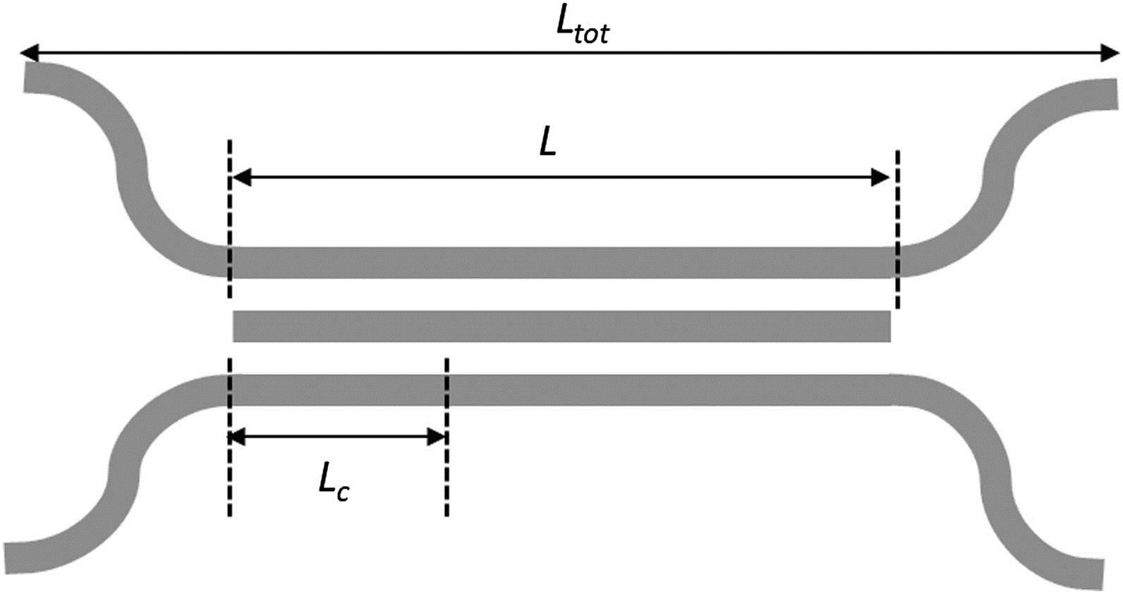
Techniques for electro-optical (EO) switching have been an ongoing concern throughout the history of integrated photonics, with the coupler being an early choice and the Mach–Zehnder interferometer (MZI) later becoming a favorite. The EO coupler approach is “revived” here and is expanded to multiple waveguides. This paper focuses on the design and numerical simulation of active broadband directional couplers consisting of three or four Si or Ge side-coupled channel waveguides. The outer two waveguides are the switching channels, and the central waveguide “island(s)” have a PIN diode structure for injecting electrons and holes into the intrinsic waveguide core(s). The active length is chosen equal to the coupling length so that input light crosses over to the second outer waveguide in the zero-bias PIN state, yielding the optical cross state. With sufficient bias applied (as determined here), the launched lightwave “decouples” and remains principally in the initial waveguide, forming the optical bar state and providing the desired crossbar switching.
Using a two-dimensional (2D) effective-index approximation of in-plane three-dimensional (3D) structures, an analytic formalism [1] and a mode-simulation software approach [2] were employed here to determine the infrared power in each waveguide as a function of propagation distance for both the voltage-off and voltage-on conditions. That modeling allowed determination of the infrared insertion loss (IL) and crosstalk (CT) at any length . The electron-and-hole concentrations and injected into an active waveguide produce a modification of the initial 0.0 bulk core index by an amount . Thus free-carrier physics comes into play to determine how the wavelength of operation and the carrier concentrations influence and . These free-carrier-effect (FCE) relationships [3] are specified here for both Si and Ge over their transparency ranges: 1.32 to 12 μm for Si and 1.8 to 12 μm for Ge. (The Ge transparency continues beyond 12 μm, but we arbitrarily stopped there.)
A level of electron-and-hole injection was selected as being an induced that is effective for switching. Although this injection level might seem “high,” it is readily reachable in practice. The EO bulk-waveguide perturbations and were then calculated from free-carrier theory at this level of injection. These perturbations were then entered into the simulation to show the switching response.
The inter-waveguide spacing enables evanescent-wave coupling of the various air-clad waveguides, and can be adjusted to determine the distance at which the first cross state occurs, which means that “any” value of can be obtained for the device such as those in the 10–4000 μm range. The change in propagation coefficient of a carrier-injected waveguide is , and we determine the two channel output powers as a function of , assuming an initial cross state. The component was fully taken into account in our work. The obtained graph is the generic switching characteristic. We found the generic characteristic of directional coupler switches composed of two, three, or four waveguides. In this paper, the abbreviations 2w, 3w, and 4w are used to denote the two-waveguide, three-waveguide, and four-waveguide directional coupler switches, respectively. The generic plots just mentioned gave us the value of required in the 2w, 3w, and 4w cases to get a reasonably low-loss bar state such as of loss. The results for 2w, 3w, and 4w were , 28, and 14, respectively. Then, starting with the -dependent FCE theory cited above, we determined a specific with which we were able to find the device length required for high-performance crossbar switching for both the Si and Ge cases. The results presented here show in the range of 0.24–0.80 mm (at ) to 1.6–3.6 mm (at ).
2. BACKGROUND DISCUSSION
The MZI may be operated as a high-performance EO switch when a pair of 3 dB couplers is employed—one at input, the other at output. The EO perturbation of active length is utilized in one arm of the MZI. This switch has the desired “cross” and “bar” states, with the cross usually occurring at perturbation-off, and with the bar state found at perturbation-on, as shown in Figs.
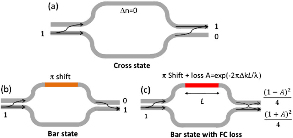
Fig. 1. MZI
For the MZI and the present 2,3,4w’s, electron–hole injection will produce a change in the complex bulk index of the intrinsic waveguide core by an amount , where is the real-index change, and is the change in extinction coefficient. The loss component is always present and is “inevitable.” If we define the ratio , we find that depends upon , , and the spectral absorption curve of Si, Ge, or SiGeSn.
The MZI has high performance and can act as a standard of comparison. The induced shift in the propagation coefficient of the MZI active waveguide is proportional to the real-index shift , and the swing in the MZI required for complete switching to the bar state is rad. During that switching, because of there will be optical propagation loss in the active arm at the bar state: , inducing IL and CT at the outputs. The normalized output power of the MZI in the presence of and phase shift is shown in Fig.
The loss parameter in Fig.
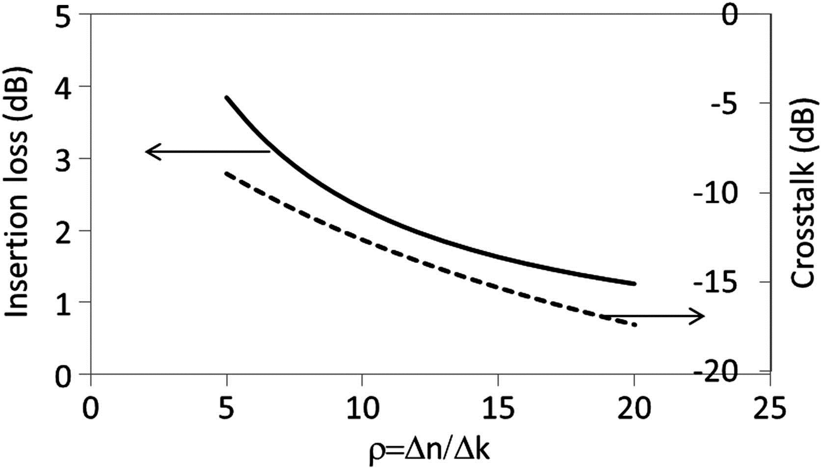
Fig. 2. MZI
This paper presents the new EO 3w and 4w as useful alternatives to the MZI. These switches are nonresonant (broad spectrum) noninterferometric devices. As shown here, complete switching appears feasible. The MZI, with its two 3 dB couplers and straight-arms section, has a “three-piece” construction, whereas our couplers offer one-piece construction. Our work here reveals a disadvantage—that the length of the 2,3,4w’s active region is always greater than that of the MZI ; however, the 2,3,4w’s overall switch length may comparable to the MZI total length. An advantage found here is that the 2,3,4w’s offer greater immunity against -induced bar-state propagation loss than do the MZIs.
The Fig.
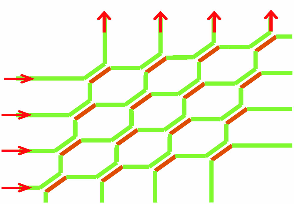
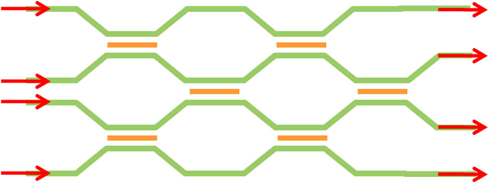
What are the possibilities? The 2w is unfortunately an asymmetric switch, because, for a given input, the switching characteristic changes when the EO zone changes from the second to the first waveguide. By contrast, the 3w and 4w have the property of being completely symmetric. Because of asymmetry, the 2w would be used functionally as a switch, and that operation works well when a group of 2w’s are “cascaded” into the crossbar matrix shown in Fig.
3. APPROACH AND ANALYSIS
Simplifying assumptions were made in the analysis. Although the actual couplers are 3D, our 2D effective-index simulations give guidelines on what to expect for the 3D case. Also, all waveguides are assumed identical—yielding synchrony or phase matching. Actually, of course, and contacts would introduce a small amount of loss in the central waveguides, thereby changing the core’s real index slightly. Hence a small IL and phase mismatch would really exist at the zero-bias cross state, violating our assumption of a perfect cross state existing at . From knowledge of and we estimate the real cross-state IL as . Here we also equate the material index change and the effective modal index change to simplify the analysis, i.e., , which is generally valid for the strongly guiding waveguide.
Our approach is divided into two parts. The analytical coupled-mode theory of Chen et al. [1] was used for the 3w, whereas the 4w research employed beam-propagation software [2] to find the infrared output power emanating from WGs 1 and 4, under varying conditions. For both devices, free-carrier theory gives effective indices in the central waveguides: at “voltage-on” and , for voltage-off.
3.3 A. Analytical Formulation for the 3w Switch
In the 3w, as shown in Fig.

Fig. 7. Top view of 3w symmetric coupler with one central active waveguide and two adjoining passive waveguides. CW light is launched from WG1.
The direct coupling between WG1 and WG3 is neglected. (This is usually true for high-index-contrast waveguides.) The optical field is launched into WG1. We are going to investigate the optical amplitude-squared , , and , the power that comes out of WGs 1, 2, and 3 respectively. We can write the following three equations to describe the light propagation within 3w:
In the present context, the zero-bias state corresponds to the case of and . Therefore, Eqs. (
Thus, by substituting into Eqs. (
3.4 B. Assumption of Weak Coupling
In arrays of parallel 3D strip waveguides, the strength of evanescent-wave coupling between adjacent waveguides is determined by the width and height of the waveguides as well as the inter-guide gap. This strength can be weak, moderate, or strong. Weak coupling is assumed here. Such coupling can be described in physical and/or mathematical language. An approximate way to talk about such coupling is to say that coupling is weak if the evanescent mode field from one waveguide does not extend into a nonadjacent waveguide.
It is difficult to state an “exact criterion” for weak coupling. A realistic way to characterize “weakness” in the present 3w and 4w cases is to say that the desired weak coupling is attained when is greater than at the wavelength of operation. Here refers to the device length needed to obtain complete cross coupling of light from one outer waveguide to the other outer waveguide when the voltage is off.
In situations in which the coupling is moderate to strong, for example, when , the same cross-to-bar switching is expected, but the IL and CT predicted by the “weak assumption” will not be accurate. Weak coupling is sometimes violated in the 7–12 μm wavelength region because the free-carrier EO effects are strong there, leading to a large perturbation that shrinks in the switching requirement. Strong coupling is not necessarily bad. Strong coupling could lead to some very good switching performance, but that analysis is beyond the scope of this paper and is recommended for future study.
3.5 C. Free-Carrier Theory
For crystalline silicon, the FCE has been worked out over the 1.3–14 μm wavelength range to yield detailed predictions of and for injected or depleted concentrations of electrons and/or holes [4]. That theory is employed here, specifically in Table
Table 1. Change in Silicon Waveguide Core Index at a Carrier Injection Level of
|
Table 2. Change in Germanium Waveguide Core Index at a Carrier Injection Level of
|
4. SWITCHING-CHARACTERISTIC RESULTS
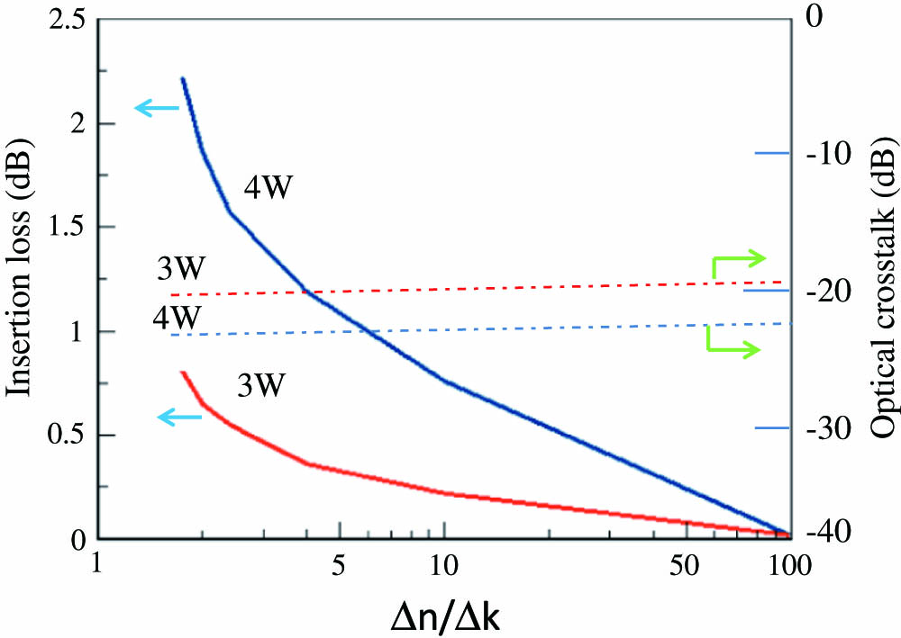
4.1 A. Comparison of 2w and 3w based on Coupled-Mode Analysis
Our first calculation is a comparison of 3w with the prior-art 2w. In the 2w, as indicated above in Fig.
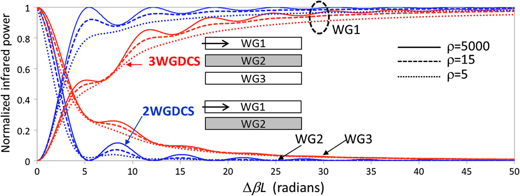
Fig. 8. “2w” and “3w”
4.2 B. Beam-Propagation Simulation for 3w and 4w
Next, beam-propagation simulation is adopted to characterize the switching performance in 3w and 4w couplers. Simulation is carried out at the TE polarization (parallel to the device plane), since the TM beam-propagation simulation is often erroneous in high-index-contrast waveguides. However, the rules deduced here apply to both polarizations. Silicon at and germanium at were chosen to examine the effects of spectrum change and materials change. Metaphorically, these choices are “end points” that “bracket” the behavior of 3w and 4w. At , a waveguide width of 0.4 μm is selected for the single-mode Si channels by scaling down the well-known width for 1.55 μm. At the upper end, the Ge width of 3.6 μm is adopted because GeSn waveguide work [7] shows widths in the range , depending upon the core/cladding index contrast.
Figure
As in the 2w and 3w cases, the bar/cross states in 4w are associated with and . Thus at fixed , the switching characteristics are determined by and . Considering the Si 4w at 1.32 μm, in order to verify that the product governs switching behavior, the responses of two devices were compared. One had , and the other had . Those lengths were attained by adjusting in each case. The cross state at for the two cases is shown by the solid lines in Fig.
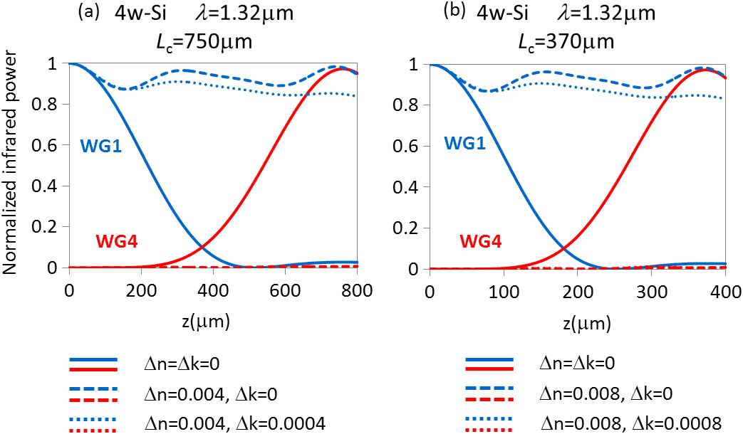
Fig. 10. Beam-propagation simulation at 1.32 μm for Si 4w with (a)
We next compare the Si 3w and 4w at 1.32 μm by considering the same with . The dependence of the power output upon is determined through beam-propagation simulation for 4w and through analytical calculation for 3w. In the lossless injection case (), ranging from 0.001 to 0.006 is introduced to give going from 4 to 25. The resulting IL and CT are plotted versus in Fig.
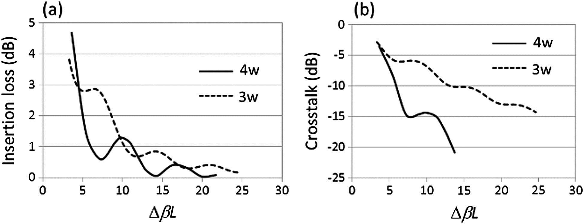
Fig. 11. (a) IL and (b) CT versus
For the remainder of this paper, the effect of finite is examined for 4w at and for 3w at . Thus, at , keeping for 4w, the for 3w is increased in Fig.
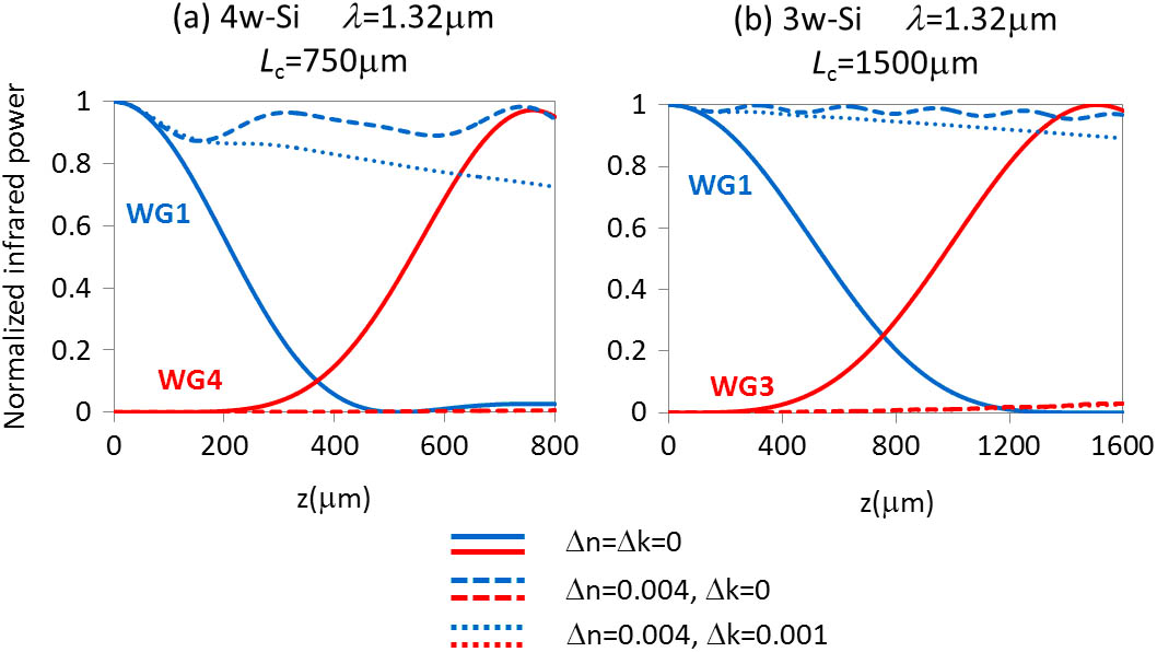
Fig. 12. Beam-propagation simulation at 1.32 μm for (a) Si 4w with
Before turning to the Ge devices, let us update the lossless Fig.
Next, as illustrated in Fig.
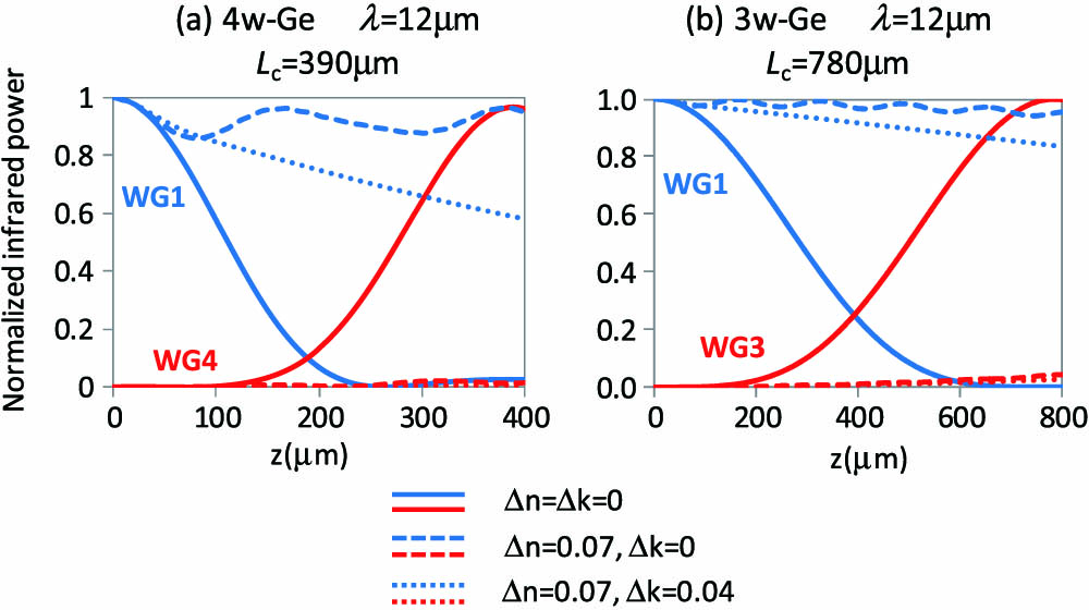
Fig. 15. Beam-propagation simulation at 12 μm for (a) Ge 4w and (b) Ge 3w at zero bias (solid lines), lossless injection (dashed lines), and lossy injection (dotted lines).
Based on the criteria for 3w and for 4w, it is straightforward to predict the minimum device length required for high-performance Si and Ge 3,4w switches at different wavelengths and at various carrier injection levels. Taking the presented in Tables
Table 3. Minimum Device Length in Si and Ge Required to Meet the
|
5. ALTERNATIVE ELECTRO-MODULATION TECHNIQUES
As viable alternatives to the FCE, there are several EO mechanisms available for altering the effective index of a semiconductor waveguide. Touching briefly on these in the present switching context, the first is the index shift induced by the Pockels effect of a DC-poled second-order nonlinear optical polymer that is embedded in a central slot of the Si or the Ge strip channel waveguide(s) in the mid-region of the 3w or 4w switch. Both “half strips” of the Si or Ge waveguide are doped for Ohmic contacting so that voltage can be applied across the EO polymer. An example is the polymer developed by the University of Arizona group [8] for the 1.55 μm wavelength (and for part of the mid-infrared). In addition, a recent paper suggests that an effective value of is feasible [9]. Let us assume that the slot contact spacing is just a few hundred nanometers. This assumption then leads to the estimate that an RF electric field of can be applied to the polymer. Then we turn to the traditional formulation: . Taking under the trade name “soluxra” with its index , we find a change of 0.0073 in the bulk polymer index. Conservatively, this should lead to an effective of 0.003 or more in the waveguide. The conclusion here is that the 4w organic-semiconductor hybrid looks quite feasible for at and for at .
The thermo-optic effect is also a good choice, mainly in Ge devices at [10] and at mid-infrared, where is about . Taking , an effective index shift around looks feasible, which could actuate a millimeter-scale 4w at . Looking at quadratic EO effects in Ge at (and in GeSn for longer wavelengths), we have the Franz–Keldysh and quantum-confined Stark effects, both of which are judged to be unlikely candidates for directional coupler switches because these effects are electro-absorption effects that have a large background absorption that would decrease the cross-state transmission.
6. PLASMONIC WAVEGUIDE COUPLERS
A new kind of channel waveguide is coming on-stream in the mid-infrared region, a strip structure that has “hybrid” waveguiding wherein a surface-plasmon-polariton mode trapped at a conductor interface [11] is combined with internal infrared reflection within a dielectric strip, forming the hybrid plasmon-polariton (HPP) mode. Experiments on this HPP strip structure at showed a large change in effective index of . However, the issue here is an initial background loss of 0.42 dB per μm. The solution to this problem is to go into the strong-coupling regime, where the switch length shrinks down to just a few wavelengths so as to minimize the initial cross-state loss. Sorger and co-workers [12,13] have presented evidence that this can be done in a 3w.
7. ACTIVE WAVEGUIDED RESONATORS
Looking to the future, the topic of EO waveguided resonators used as the central waveguide(s) in 3w and 4w is ripe for exploration. The Si or Ge strip waveguide can be made resonant by forming an inline array of cylindrical holes or rectangular slots in the waveguide so as to create a one-dimensional photonic crystal (PhC) cavity having reasonably high . Such a resonator is known as a nanobeam (NB), and this PhC device is quite scaleable with wavelength. The FCEs are quite applicable to NBs and can cause considerable shift and damping of a particular resonant mode by the depletion, injection, or accumulation of charge. For example, a recent paper [14] pointed out the advantages of using a lateral PN junction to deplete a 1.55 μm group IV NB. The technique of resonance shifting within 3w and 4w is expected to yield switch lengths that are much smaller than those derived here for broadband structures. The much-reduced device size in the cavity cases comes at the expense of a narrow spectral window.
8. CONCLUSION
The 2D effective-index approximation allows us to sketch out the main features of actual 3D directional coupler switches that are integrated in plane with side-coupled parallel channels. An analytic coupled-mode formalism was taken for 3w, and a beam-propagation software numerical-simulator approach was taken for 4w. All three devices, 2w, 3w, and 4w, are readily cascadeable into the crossbar matrix switch. Unlike the asymmetric 2w, the symmetric 3ws and 4ws are easily cascaded into the nonblocking permutation matrix switch. The 4w is generally more compact than either 3w or 2w since it does not always require spatial “fan out” of the outer waveguides.
In the 3w,4w analysis, phase-matched synchrony of WGs in the weak-coupling regime is assumed, resulting in a perfect cross state with injection off. (In reality, this cross state has a small IL due to the background loss of the WGs.) Our simulations for silicon show the new result that the bar state with injection on is well shielded from IL induced by the component. Silicon 3w’s and 4w’s are projected to give bar-state IL and CT over the full 1.3–12 μm wavelength range when the PIN injection level is chosen to yield an index change of for the 3w and for the 4w. This simulation takes into account the actual loss that accompanies the . Generally, the 4w can achieve switching performance equivalent to 3w in half of the 3w’s length, but the bar-3w is less sensitive to as compared to bar-4w. It is clear that 3w, 4w have a significantly larger active length when compared to the reference MZI active length whose switching requirement is . However, the MZI is not protected against bar-state IL loss linked to , which would be in the MZI during the presence of . At that same level, the IL for 4w is only 0.8 dB. As mentioned, the cross state at zero bias would experience contact loss from P and N doping, but that loss is expected to be small in practice.
For the free-carrier scenario, switching speed and energy consumption were not addressed here. Instead, theoretical estimates of CT and IL were targeted. The projected performance is “good” for the following reasons: the bar state CT was less than for Si and Ge, in both 3w and 4w. The bar state IL depended upon ρ, which ranged from 5.3 to 17.8 for Si and from 1.5 to 4.8 for Ge. Analysis of Si over the 1.32–12 μm range, and of Ge over the 1.8–12 μm range, gave IL of 0.30 to 0.55 dB in Si 3w, 0.65 to 1.0 dB in Si 4w, 0.7 to 1.6 dB in Ge 3w, and 1.2 to 2.2 dB in Ge 4w. Those losses are low except for the 2.2 dB longwave loss in Ge 4w.
A benefit of PIN-waveguide free-carrier injection is the decreased switch length in the mid-wave and long-wave infrared regions. That happens because FCE grows stronger with increasing wavelength. If a representative injection is assumed, and if is raised from 1.32 to 12 μm, then decreases from 3.6 to 0.49 mm (Si 3w), from 1.8 to 0.24 mm (Si 4w), from 3.2 to 0.8 mm (Ge 3w), and from 1.6 to 0.4 mm (Ge 4w).
It is likely that improvements in switching performance for these Si and Ge devices can be attained by selecting a different EO mechanism, by choosing plasmonic EO waveguides (instead of photonic waveguides), or by inserting cavity resonators within active photonic waveguides. For example, analysis indicates that a fast, low-loss EO polymer “slot layer” embedded in a Si or Ge strip waveguide would yield low-loss switching in a 1 mm length at and in a 3 mm length at .
9 ACKNOWLEDGMENTS
Acknowledgment. The author appreciates the valuable help of Dr. Yijing Chen (Data Storage Institute of Singapore and the ECE Dept., National University of Singapore), who performed all of the Beam Prop simulations. Dr. Chen’s wisdom and technical advice were essential to this paper. Support of the Air Force Office of Scientific Research (Dr. Gernot Pomrenke, Program Manager) and the UK Engineering and Physical Sciences Research Council (Project MIGRATION) is also gratefully acknowledged.
[2]
[3] R. A. Soref, L. Friedman. Electrooptical modulation in Si1-xGex/Si and related heterostructures. Int. J. Optoelectron., 1994, 9: 205-210.
[6] R. A. Soref, D. L. McDaniel, B. R. Bennett. Guided-wave intensity modulators using amplitude and phase perturbations. IEEE J. Lightwave Technol., 1988, LT-6: 437-443.
Article Outline
Richard Soref. Mid-infrared 2 × 2 electro-optical switching by silicon and germanium three-waveguide and four-waveguide directional couplers using free-carrier injection[J]. Photonics Research, 2014, 2(5): 05000102.
