光学学报, 2017, 37 (12): 1202001, 网络出版: 2018-09-06
一种光学通道开放且适合构建晶格的静电阱  下载: 567次
Electrostatic Trap Suitable for Construction of Lattices with Opened Optical Access
图 & 表
图 1. (a) 三个带电球电极囚禁分子的方案图; (b) 镜像法的原理图
Fig. 1. (a) Schematic for trapping molecules using three charged spherical electrodes; (b) schematic of the image method
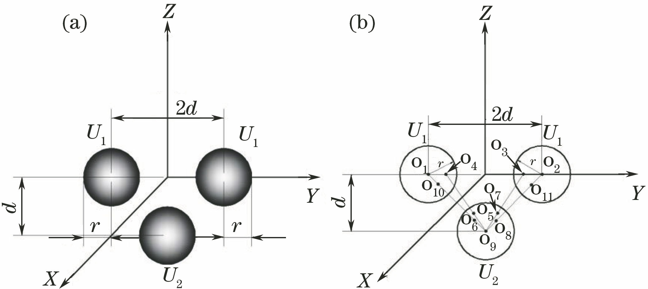
图 2. 囚禁时YOZ、XOZ、XOY平面的电场等高线分布的解析解和数值解。(a)(d) YOZ平面; (b)(e) XOZ平面; (c)(f) XOY平面
Fig. 2. Analytical solutions and numerical solutions of contour distributions of trapping field at YOZ, XOZ and XOY planes. (a)(d) YOZ plane; (b)(e) XOZ plane; (c)(f) XOY plane
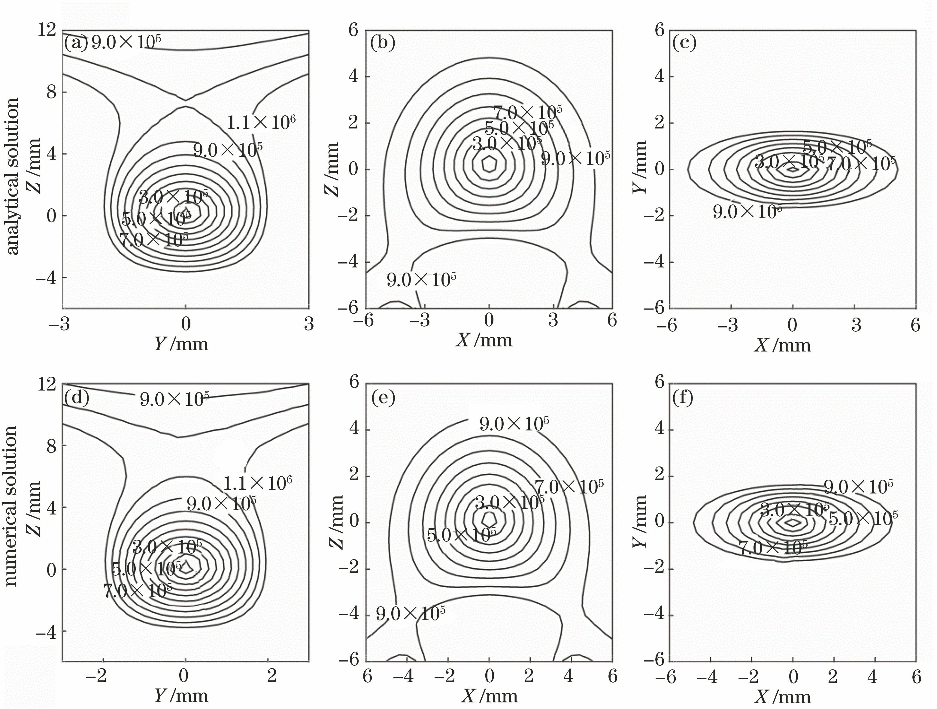
图 4. 沿Z方向的电场分布及对处于量子态|J,K,M>=|1,1,-1>的ND3分子的Stark势能。 (a)装载; (b)囚禁
Fig. 4. Electric field distributions in Z direction and Stark potential for ND3 molecules in state (|J,K,M>=|1,1,-1>). (a) Loading; (b) trapping
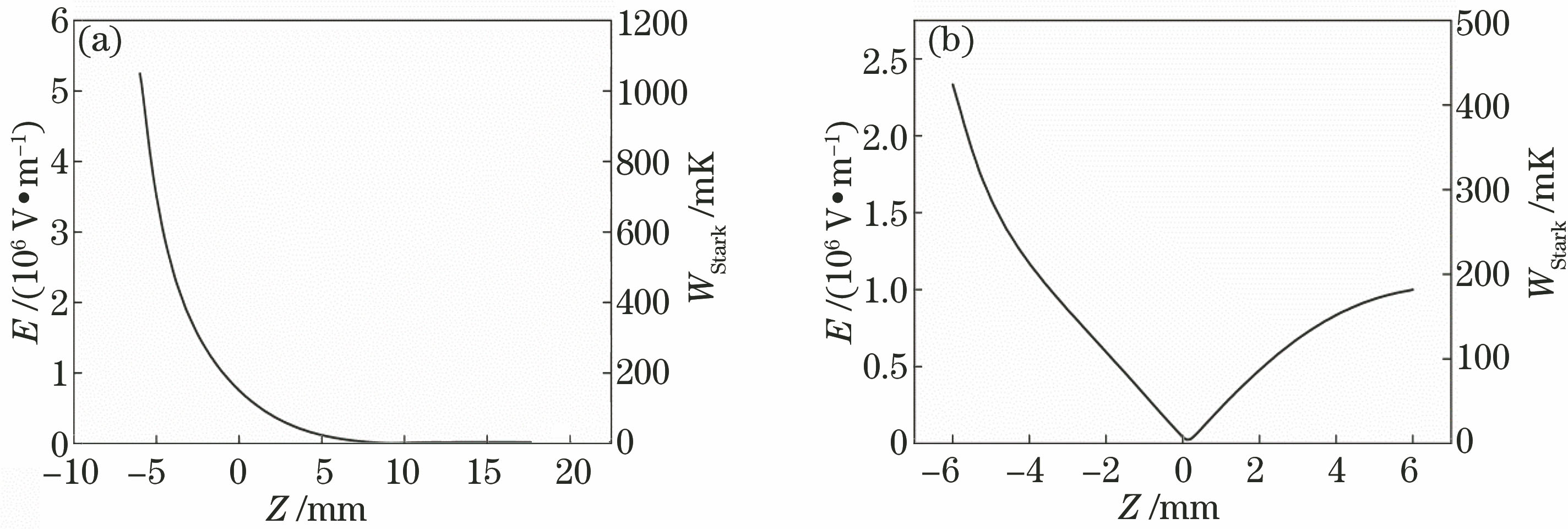
图 5. 在三个不同分子束入射速度下,装载效率与装载时间的关系
Fig. 5. Relationship between loading efficiency and loading time under different velocities of incident molecular beam
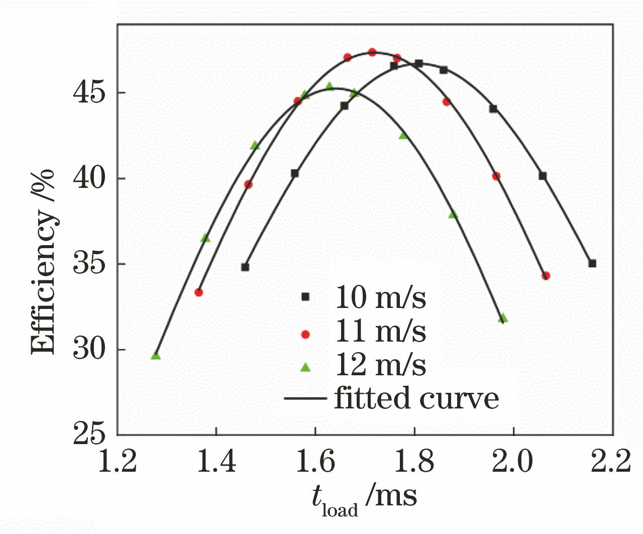
图 6. 装载效率与入射分子束中心速度的关系
Fig. 6. Relationship between loading efficiency and center velocity of incident molecular beam
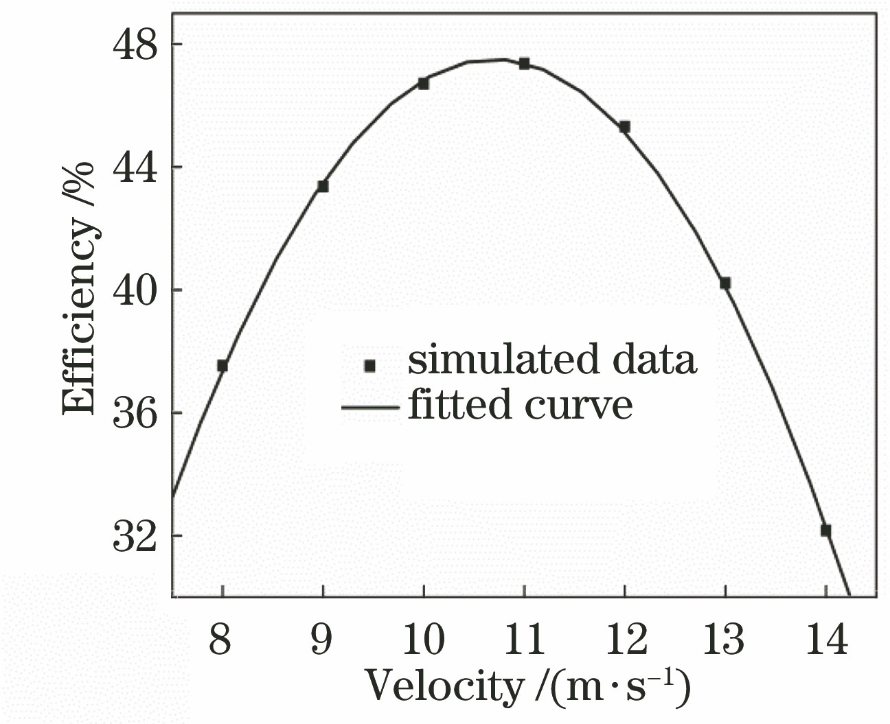
图 7. 入射分子束的初始速度分布及囚禁在阱中的分子速度(VX、VY、VZ)分布。 (a) VX; (b) VY; (c) VZ
Fig. 7. Velocity distributions of incident molecular beam before loading process and the trapped cold molecules. (a) VX; (b) VY; (c) VZ
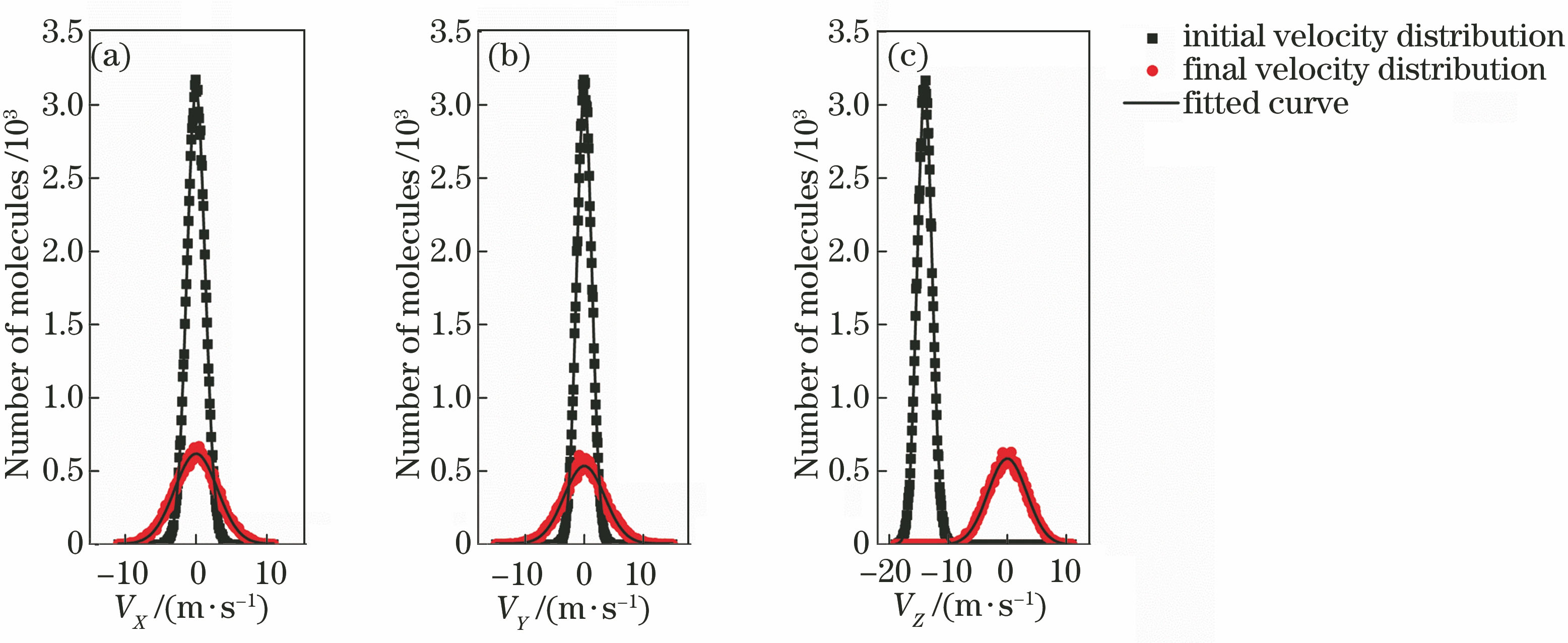
图 8. 用三个带电球电极构建静电表面阱方案图
Fig. 8. Schematic for trapping molecules on a chip with three charged spherical electrodes
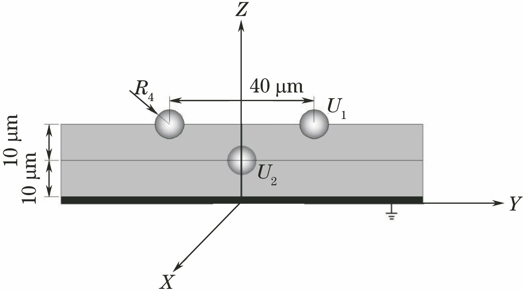
图 9. 囚禁电场的等高线分布。 (a) YOZ平面; (b) XOZ 平面; (c) XOY平面
Fig. 9. Contour distributions of trapping field. (a) YOZ plane; (b) XOZ plane; (c) XOY plane
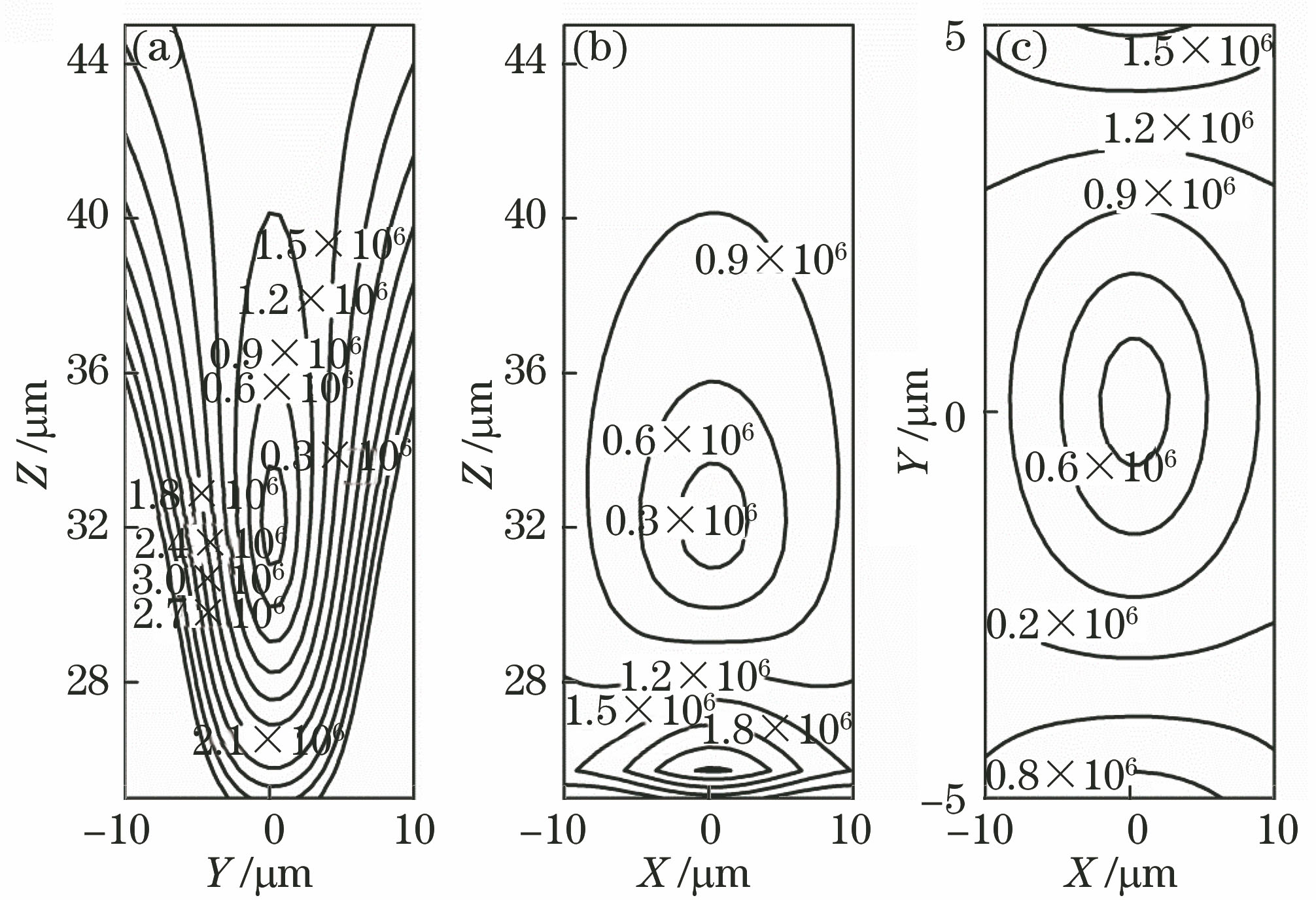
图 10. 一系列三球电极实现在芯片表面对冷分子静电囚禁(一维静电晶格)
Fig. 10. Schematic for trapping molecules on a chip with a series of three charged spherical electrodes (one-dimensional electrostatic lattice)
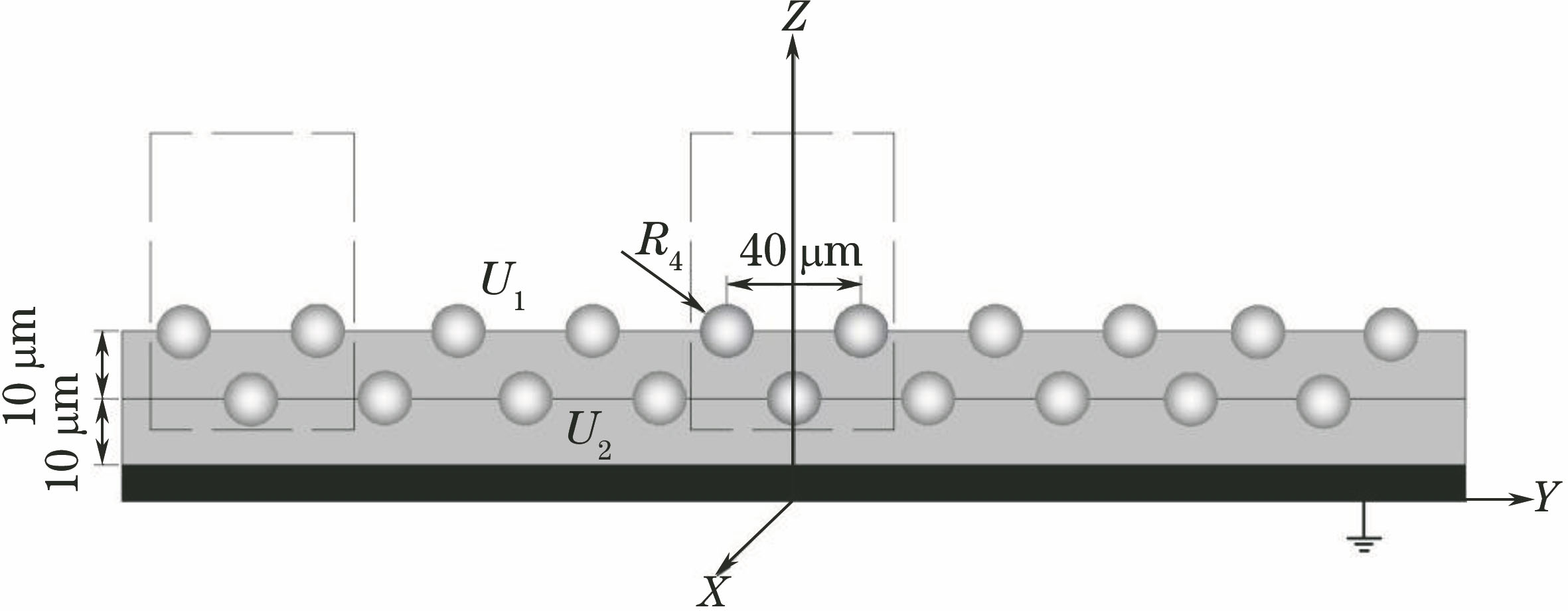
图 11. 在两个不同位置处[图9(a)虚框位置]电场的等高线分布。 (a)(d) XOZ平面; (b)(e) XOY平面; (c)(f) YOZ平面
Fig. 11. Contour distributions of trapping field at two different locations [marked with dashed box in Fig. 9(a)]. (a)(d) XOZ plane; (b)(e) XOY plane; (c)(f) YOZ plane

图 12. 利用一系列三球电极在芯片表面实现对冷分子的静电囚禁(二维静电晶格)
Fig. 12. Schematic for electrostatic trapping of cold molecules on a chip with a series of three charged spherical electrodes (two-dimensional electrostatic lattice)
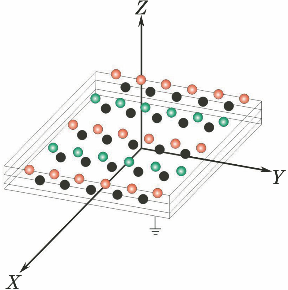
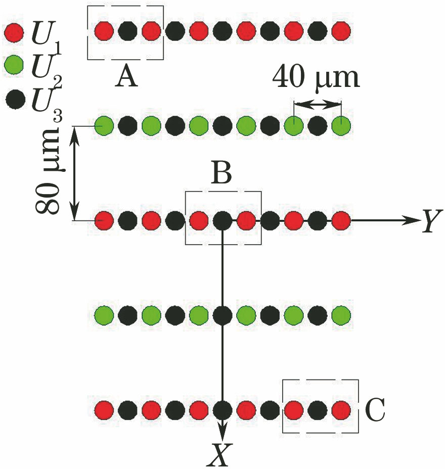

表 1电荷量和坐标
Table1. Charges and coordinates
|
李胜强, 张梦芝, 杨亮亮. 一种光学通道开放且适合构建晶格的静电阱[J]. 光学学报, 2017, 37(12): 1202001. Shengqiang Li, Mengzhi Zhang, Liangliang Yang. Electrostatic Trap Suitable for Construction of Lattices with Opened Optical Access[J]. Acta Optica Sinica, 2017, 37(12): 1202001.


 PDF全文
PDF全文

