1 1.昆明理工大学 材料科学与工程学院,昆明 650031
2 2.塔什干都灵工业大学, 塔什干 100095, 乌兹别克斯坦
光催化以其反应条件温和、能直接利用太阳能转化为化学能的优势, 而备受科研人员的关注。如何拓展光谱吸收范围及阻止光生“电子-空穴”复合, 是目前光催化研究领域的热点。本工作通过阳极氧化制备出非晶TiO2纳米管(TiO2NTs), 利用机械液压法将熔融铟锡合金压入非晶TiO2中, 得到In9.45Sn1/TiO2NTs, 再经高温煅烧后得到ITO/TiO2NTs复合材料。实验对比了TiO2NTs、In9.45Sn1/TiO2NTs与ITO/TiO2NTs对去除水溶液中亚甲基蓝的光催化性能, 在180 min光照下, ITO/TiO2NTs的降解效果最佳, 降解效率达96.14%。利用紫外-可见漫反射光谱(UV-Vis DRS)研究了TiO2NTs、In9.45Sn1/TiO2NTs和ITO/TiO2NTs的光吸附性能, ITO/TiO2NTs的吸光度最强。结合瞬态光电流响应、光电流密度电势、电化学阻抗谱和Mott-Schottky测试结果可知, ITO/TiO2NTs比TiO2NTs具有更高的电荷转移能力和供体密度, 抑制了空穴和电子的复合, 从而增强光电化学性能。经过五次循环后, ITO/TiO2NTs的降解效率保持在90.28%。自由基捕获实验结果表明, •O2-和•OH是光催化降解的主要活性物质。
二氧化钛 ITO 纳米管阵列 亚甲基蓝 机械液压法 titania ITO nanotube array methylene blue mechanical hydraulic method
1 上海理工大学光电信息与计算机工程学院, 上海 200093
2 教育部光学仪器与系统工程研究中心, 上海市现代光学系统重点实验室, 上海 200093
本文通过电子束蒸发技术制备了金属锡掺杂浓度不同的一系列ITO薄膜。采用X射线衍射仪、原子力显微镜、紫外-可见光-近红外分光光度计、四探针测电阻仪和Z扫描系统分别对ITO薄膜的物相结构、微观形貌、光学吸收、方块电阻和非线性光学性能进行测试和表征。结果表明, 随着金属锡掺杂浓度由10%增加到30%: ITO薄膜的结晶质量增加; 薄膜表面粗糙度增加, 晶粒尺寸逐渐增大; 等离子体吸收增强, 且吸收峰的位置发生红移, 光学带隙变窄; 薄膜的方块电阻不断减小; 非线性吸收系数逐渐增加, 绝对值最大可以增至2.59×10⁻⁷ cm/W。时域有限差分拟合结果表明金属锡掺杂浓度不同的ITO薄膜电场强度变化规律与实验结果相一致。
氧化铟锡 局部表面等离子体共振 非线性光学响应 Z扫描 增强电场 掺杂 电子束蒸发 ITO LSPR nonlinear optical response Z-scan enhanced electric field doping electron beam evaporation
1 中国科学技术大学国家示范性微电子学院,合肥 230026
2 中国科学院苏州纳米技术与纳米仿生研究所,苏州 215123
3 苏州纳维科技股份有限公司,苏州 215123
4 江苏第三代半导体研究院,苏州 215000
透明半导体铟锡氧化物(ITO)作为电极能够降低光导开关电极边缘电流集聚效应和提高脉冲激光的利用率。本文通过在ITO与GaN界面之间分别插入10 nm的Ti与TiN, 研究Ti、TiN对ITO与GaN欧姆接触性能的影响。I-V测试结果表明, 随着退火温度升高, 插入TiN的光导开关一直保持欧姆接触特性, 而插入Ti的光导开关由欧姆接触转变为肖特基接触。通过TEM测试发现, 当以Ti作为插入层时, ITO通过插入层向插入层与GaN的界面扩散, 在接触界面形成Ti的氧化物及空洞。透射光谱显示, 不同退火温度下插入Ti层的透过率均低于38.3%, 而以TiN作为插入层时透过率为38.8%~55.0%。因此含有TiN的光导开关具有更稳定的电学性能和更高的透过率, 这为GaN光导开关在高温高功率领域的应用提供了参考。
GaN光导开关 欧姆接触 GaN photoconductive semiconductor switch ITO ITO Ti Ti TiN TiN Ohmic contact

Author Affiliations
Abstract
Engineering Research Center of Optical Instrument and System, Ministry of Education and Shanghai Key Laboratory of Modern Optical System, University of Shanghai for Science and Technology, Shanghai 200093, China
In this study, a batch of indium tin oxide (ITO)/Sn composites with different ratios was obtained based on the principle of thermal evaporation by an electron beam. The crystalline structure, surface shape, and optical characterization of the films were researched using an X-ray diffractometer, an atomic force microscope, a UV-Vis-NIR dual-beam spectrophotometer, and an open-hole Z-scan system. By varying the relative thickness ratio of the ITO/Sn bilayer film, tunable nonlinear optical properties were achieved. The nonlinear saturation absorption coefficient maximum of the ITO/Sn composites is , approximately 21 and 1.72 times more enhanced compared to monolayer ITO and Sn, respectively. Moreover, the improvement of the sample nonlinear performance was verified using finite-difference in temporal domain simulations.
ITO/Sn composite film Z-scan nonlinear absorption characteristic synergistic effect electric field enhancement Chinese Optics Letters
2023, 21(8): 081902
Author Affiliations
Abstract
1 State Key Laboratory of Precision Spectroscopy, School of Physics and Electronic Science, East China Normal University, Shanghai 200062, China
2 Huawei Technologies Co, Ltd., Bantian Longgang District, Shenzhen 518129, China
3 Collaborative Innovation Center of Extreme Optics, Shanxi University, Taiyuan 030006, China
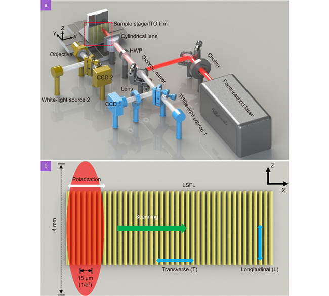
This paper reports the fabrication of regular large-area laser-induced periodic surface structures (LIPSSs) in indium tin oxide (ITO) films via femtosecond laser direct writing focused by a cylindrical lens. The regular LIPSSs exhibited good properties as nanowires, with a resistivity almost equal to that of the initial ITO film. By changing the laser fluence, the nanowire resistances could be tuned from 15 to 73 kΩ/mm with a consistency of ±10%. Furthermore, the average transmittance of the ITO films with regular LIPSSs in the range of 1200–2000 nm was improved from 21% to 60%. The regular LIPSS is promising for transparent electrodes of nano-optoelectronic devices—particularly in the near-infrared band.
transparent nanowires periodic surface nanostructures femtosecond laser direct writing ITO film anisotropic electrical conductivity Opto-Electronic Science
2023, 2(1): 220002
闽南师范大学物理与信息工程学院,福建 漳州 363000
铟锡氧化物(ITO)作为一种高掺杂的半导体材料,其材料介电常数零点波长位于近红外波段,且其在近红外波段的吸收损耗较小,因此ITO可以成为近红外波段理想的局域表面等离激元共振效应(LSPR)材料。采用时域有限差分法模拟长方体状ITO纳米棒阵列的LSPR效应,通过调整ITO纳米棒的载流子浓度、尺寸、间距以及衬底折射率实现其红外波段LSPR共振峰的有效调节。这对于扩宽ITO纳米结构在红外波段LSPR效应的应用具有重要的研究意义。
材料 局域表面等离激元共振 ITO纳米结构 时域有限差分法 消光特性

Author Affiliations
Abstract
1 Institute of Semiconductors, Chinese Academy of Sciences, Beijing 100083, China
2 Beijing Smart-chip Microelectronics Technology Co., Ltd, Beijing 100083, China
3 Zhongguancun Xinhaizeyou Technology Co., Ltd, Beijing 100049, China
4 Center of Materials Science and Optoelectronics Engineering, University of Chinese Academy of Sciences, Beijing 100049, China
The silicon on glasses process is a common preparation method of micro-electro-mechanical system inertial devices, which can realize the processing of thick silicon structures. This paper proposes that indium tin oxides (ITO) film can serve as a deep silicon etching cut-off layer because ITO is less damaged under the attack of fluoride ions. ITO has good electrical conductivity and can absorb fluoride ions for silicon etching and reduce the reflection of fluoride ions, thus reducing the foot effect. The removal and release of ITO use an acidic solution, which does not damage the silicon structure. Therefore, the selection of the sacrificial layer has an excellent effect in maintaining the shape of the MEMS structure. This method is used in the preparation of MEMS accelerometers with a structure thickness of 100 μm and a feature size of 4 μm. The over-etching of the bottom of the silicon structure caused by the foot effect is negligible. The difference between the simulated value and the designed value of the device characteristic frequency is less than 5%. This indicates that ITO is an excellent deep silicon etch stopper material.The silicon on glasses process is a common preparation method of micro-electro-mechanical system inertial devices, which can realize the processing of thick silicon structures. This paper proposes that indium tin oxides (ITO) film can serve as a deep silicon etching cut-off layer because ITO is less damaged under the attack of fluoride ions. ITO has good electrical conductivity and can absorb fluoride ions for silicon etching and reduce the reflection of fluoride ions, thus reducing the foot effect. The removal and release of ITO use an acidic solution, which does not damage the silicon structure. Therefore, the selection of the sacrificial layer has an excellent effect in maintaining the shape of the MEMS structure. This method is used in the preparation of MEMS accelerometers with a structure thickness of 100 μm and a feature size of 4 μm. The over-etching of the bottom of the silicon structure caused by the foot effect is negligible. The difference between the simulated value and the designed value of the device characteristic frequency is less than 5%. This indicates that ITO is an excellent deep silicon etch stopper material.
SOG process DRIE cut-off layer ITO film foot effect Journal of Semiconductors
2023, 44(4): 044101
为了满足ITO玻璃深加工生产线的掰断和输送的工艺需求,设计了一种ITO玻璃带负压换向掰断输送设备,解决了不同于普通玻璃的ITO玻璃深加工生产线现场问题。
ITO玻璃生产线 负压 换向 掰断 输送 ITO glass production line negative pressure reversing breaking delivery
1 桂林电子科技大学材料科学与工程学院,电子信息材料与器件教育部工程研究中心,广西信息材料重点实验室,桂林 541004
2 广西中沛光电科技有限公司,来宾 546100
本文采用直流磁控溅射分层溅射制备了氧化铟锡(ITO)/银(Ag)/ITO多层复合薄膜。系统研究了溅射温度对ITO/Ag/ITO多层复合薄膜的结构和光电性能影响。采用ITO(m(In2O3)∶m(SnO2)=9∶1; 直径60 mm)靶材和Ag(纯度99.999%; 直径60 mm)靶材分层溅射,使ITO薄膜和Ag薄膜依次沉积在钠-钙玻璃基片上。结果表明,溅射温度对该薄膜的形貌和结构具有显著的影响。在中间Ag薄膜和顶层ITO薄膜的溅射温度均为120 ℃时,薄膜表面晶粒形貌由类球形转变为菱形,此时薄膜方阻为3.68 Ω/Sq,在488 nm处透射率为88.98%,且品质因数为0.03 Ω-1,实现了低方阻高可见光透射率ITO/Ag/ITO多层复合薄膜的制备。
磁控溅射 分层溅射 复合薄膜 ITO薄膜 Ag薄膜 溅射温度 megnetron sputtering hierarchical sputtering composite film ITO thin film Ag thin film sputtering temperature


