中国石油大学(华东)理学院,山东 青岛 266580
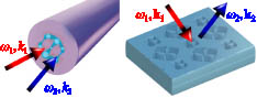
具有超高品质因子的光学微腔是构造各种集成光子器件的重要组件,以光子晶体微腔为基础的混合微腔为实现强烈的光和物质相互作用提供了一个新颖的平台,在腔量子电动力学、集成单光子源、量子计算等方面都具有十分广阔的应用前景。本文基于双异质结构光子晶体微腔,结合蝶形金纳米天线等离激元结构,设计实现了一种可见光波段的新型光子-等离激元混合微腔,并通过改变蝶形金纳米天线的间隙、角度、长度、厚度、相对位置等结构参数,利用三维时域有限差分法研究了等离激元纳米结构对混合腔的品质因子、有效模式体积、品质因数的调控规律,模拟结果显示,混合腔的有效模式体积和品质因数分别始终稳定在10-6(λ/n)3和108(λ/n)-3数量级,最佳品质因数值可达5.730689×108(λ/n)-3,优于其他类型的微腔。
光电子学 纳米光子学和光子晶体 光子晶体微腔 等离激元 纳米天线 品质因子 时域有限差分法 激光与光电子学进展
2023, 60(15): 1525002

Author Affiliations
Abstract
1 Key Laboratory of Artificial Structures and Quantum Control (Ministry of Education), Shanghai 200240, China
2 School of Physics and Astronomy, Shanghai Jiao Tong University, Shanghai 200240, China
3 Collaborative Innovation Center of Advanced Microstructures, Nanjing 210000, China
We propose an optical weighing technique with a sensitivity down to a single atom through the coupling between a surface plasmon and a suspended graphene nanoribbon resonator. The mass is determined via the vibrational frequency shift on the probe absorption spectrum while the atom attaches to the nanoribbon surface. We provide methods to separate out the signals of the ultralow frequency vibrational modes from the strong Rayleigh background, first based on the quantum coupling with a pump-probe scheme. Owing to the spectral enhancement in the surface plasmon and the ultralight mass of the nanoribbon, this scheme results in a narrow linewidth (~GHz) and ultrahigh mass sensitivity (~30 yg). Benefitting from the low noises, our optical mass sensor can be achieved at room temperature and reach ultrahigh time resolution.
Optomechanics Surface plasmons Nanophotonics and photonic crystals Spectroscopy, atomic Photonics Research
2018, 6(9): 09000867

Author Affiliations
Abstract
1 School of Information and Communication Engineering, Beijing University of Posts and Telecommunications, Beijing 100876, China
2 State Key Laboratory of Information Photonics and Optical Communications, Beijing University of Posts and Telecommunications, Beijing 100876, China
3 State Key Laboratory for Mesoscopic Physics, School of Physics, Peking University, Collaborative Innovation Center of Quantum Matter, Beijing 100871, China
4 Collaborative Innovation Center of Extreme Optics, Shanxi University, Taiyuan, Shanxi 030006, China
Optical trapping techniques are of great interest since they have the advantage of enabling the direct handling of nanoparticles. Among various optical trapping systems, photonic crystal nanobeam cavities have attracted great attention for integrated on-chip trapping and manipulation. However, optical trapping with high efficiency and low input power is still a big challenge in nanobeam cavities because most of the light energy is confined within the solid dielectric region. To this end, by incorporating a nanoslotted structure into an ultracompact one-dimensional photonic crystal nanobeam cavity structure, we design a promising on-chip device with ultralarge trapping potential depth to enhance the optical trapping characteristic of the cavity. In this work, we first provide a systematic analysis of the optical trapping force for an airborne polystyrene (PS) nanoparticle trapped in a cavity model. Then, to validate the theoretical analysis, the numerical simulation proof is demonstrated in detail by using the three-dimensional finite element method. For trapping a PS nanoparticle of 10 nm radius within the air-slot, a maximum trapping force as high as 8.28 nN/mW and a depth of trapping potential as large as 1.15×10⁵ kBT mW 1 are obtained, where kB is the Boltzmann constant and T is the system temperature. We estimate a lateral trapping stiffness of 167.17 pN·nm 1· mW 1 for a 10 nm radius PS nanoparticle along the cavity x-axis, more than two orders of magnitude higher than previously demonstrated on-chip, near field traps. Moreover, the threshold power for stable trapping as low as 0.087 μW is achieved. In addition, trapping of a single 25 nm radius PS nanoparticle causes a 0.6 nm redshift in peak wavelength. Thus, the proposed cavity device can be used to detect single nanoparticle trapping by monitoring the resonant peak wavelength shift. We believe that the architecture with features of an ultracompact footprint, high integrability with optical waveguides/circuits, and efficient trapping demonstrated here will provide a promising candidate for developing a lab-on-a-chip device with versatile functionalities.
Integrated optics devices Nanophotonics and photonic crystals Optical tweezers or optical manipulation Laser trapping Photonic crystals Resonators Photonics Research
2018, 6(2): 02000099
Author Affiliations
Abstract
1 Department of Electrical Engineering, Princeton University, Princeton, New Jersey 08544, USA
2 John A. Paulson School of Engineering and Applied Sciences, Harvard University, Cambridge, Massachusetts 02138, USA
Typically, photonic waveguides designed for nonlinear frequency conversion rely on intuitive and established principles, including index guiding and bandgap engineering, and are based on simple shapes with high degrees of symmetry. We show that recently developed inverse-design techniques can be applied to discover new kinds of microstructured fibers and metasurfaces designed to achieve large nonlinear frequency-conversion efficiencies. As a proof of principle, we demonstrate complex, wavelength-scale chalcogenide glass fibers and gallium phosphide three-dimensional metasurfaces exhibiting some of the largest nonlinear conversion efficiencies predicted thus far, e.g., lowering the power requirement for third-harmonic generation by 104 and enhancing second-harmonic generation conversion efficiency by 107. Such enhancements arise because, in addition to enabling a great degree of tunability in the choice of design wavelengths, these optimization tools ensure both frequency- and phase-matching in addition to large nonlinear overlap factors.
Computational electromagnetic methods Nonlinear optics, fibers Harmonic generation and mixing Nonlinear optics, devices Nanophotonics and photonic crystals Photonics Research
2018, 6(5): 05000B82

Author Affiliations
Abstract
1 School of Physics & Astronomy, University of Birmingham, Birmingham B15 2TT, UK
2 Center for Terahertz Waves and College of Precision Instrument and Optoelectronics Engineering, Tianjin University, Tianjin 300072, China
Indefinite media with mixed signs of dielectric tensor elements possess unbounded equifrequency surfaces that have been utilized for diverse applications such as superimaging, enhanced spontaneous emission, and thermal radiation. One particularly interesting application of indefinite media is an optical cavity supporting anomalous scaling laws. In this Letter, we show that by replacing an indefinite medium with magnetized plasma one can construct a tunable indefinite cavity. The magnetized plasma model is based on realistic semiconductor material properties at terahertz frequencies that show hyperbolic dispersion in a certain frequency regime. The hyperbolic dispersion features are utilized for the design of optical cavities. Dramatically different sizes of cavities can support the same resonance mode at the same frequency. For a cavity of fixed size, the anomalous scaling law between the resonance frequency and mode number is confirmed. The resonance frequency can be strongly modulated by changing the strength of the applied magnetic field. The proposed model provides active controllability of terahertz resonances on the deep subwavelength scale with realistic semiconductor materials.
350.4238 Nanophotonics and photonic crystals 350.5400 Plasmas Chinese Optics Letters
2018, 16(5): 050005

Author Affiliations
Abstract
1 Microelectronics-Photonics Graduate Program, University of Arkansas, Fayetteville, Arkansas 72701, USA
2 Department of Physics, University of Arkansas, Fayetteville, Arkansas 72701, USA
Plasmonic grating structures have been shown effective at increasing near-field optical enhancement. A doublewidth plasmonic grating design is introduced, where each period has two alternating metal widths separated by a nanogap. With this new design, analysis has shown that plasmonic resonances couple between each metal section, resulting in even greater optical enhancement compared with single-width gratings. The geometry that gives the greatest optical enhancement has been determined with a computational model. This work demonstrates that the increased enhancement is due to hybridized modes that couple between the two grating segments.
Surface plasmons Surface plasmons Plasmonics Plasmonics Gratings Gratings Nanophotonics and photonic crystals. Nanophotonics and photonic crystals. Photonics Research
2016, 4(5): 05000173
Author Affiliations
Abstract
Centre for Micro-Photonics, Faculty of Engineering and Industrial Sciences, Swinburne University of Technology, Hawthorn VIC 3122, Australia
We demonstrate the confinement of broadband optical energy in the visible to near-infrared regime in a threedimensional nanoscale volume with high energy efficiency in a nanostructure consisting of multiple nanoslits in dielectric chacolgenide material. We find that a broadband optical field can be confined down to the scale of 1 nm (λ∕650) with a confinement volume of λ3∕3 × 10<参考文献原文>The figure of merit of the nanostructure can be up to 10 times that achieved by plasmonic lensing and nanofocusing. Our work opens a new way for truly nanoscaled photonics applicable to nanolithograpy, nanoimaging, lab-on-chip nanosensing, single-molecule detection, and nanospectroscopy.
Subwavelength structures nanostructures Nanophotonics and photonic crystals Photonics Research
2013, 1(3): 03000136
Author Affiliations
Abstract
Introducing the finite difference time domain method and perfect match layer absorbing boundary condition, the electro-tunable localized modes in two-dimensional (2D) nematic-liquid-crystal photonic crystal with a point defect (1PD2D-NLCPC) are investigated by numerical simulation. The numerical simulations show that as the direction of the external electrical field varies, the band gap in the 1PD2D-LCPC changes; when the wavelength in the band gap is the wavelength of the sine source wave, the most of optical field energy is localized in the point defect; therefore manipulating the direction of the external electrical field causes the change of the localized mode.
160.0160 Materials 160.5298 Photonic crystals 350.0350 Other areas of optics 350.4238 Nanophotonics and photonic crystals Chinese Optics Letters
2012, 10(s2): S21602
Author Affiliations
Abstract
To resolve the problem of missed evanescent waves in a beam focusing system, a hyperlens-based beam focusing device is proposed in this letter. This device can convert the evanescent waves into propagating waves, and then a super-resolution spot is formed at the center of the hyperlens. The working principle of the device is presented, and the way in which the material and structural parameters of the hyperlens affect the resolution and transmission is analyzed in detail. A multibeam focusing device is optimally designed, and the simulated results verify that a nanoscale spot with a diameter of 15.6 nm (corresponding to \lambda 0/24, where \lambda 0 is the working wavelength in vacuum) is achieved, which is far less than the diffraction limited resolution with a value of 625 nm (1.7\lambda 0). The device is expected to find numerous applications in optical data storage and nano{photolithography, among others.
230.0230 Optical devices 160.3918 Metamaterials 220.3630 Lenses 350.4238 Nanophotonics and photonic crystals Chinese Optics Letters
2012, 10(4): 042302
Author Affiliations
Abstract
1 Physics Department of the Science College, China University of Mining and Technology, Xuzhou 221116, China
2 Surface Physics Laboratory, Fudan University, Shanghai 200433, China
We propose a two-dimensional (2D) annular photonic crystal (APC) with dual equi-frequency contours (EFCs) in one band. The refractive behaviors of a Gaussian beam incident from air to the APC are analyzed by the EFC analysis and finite-difference time-domain (FDTD) method. The results show the positive-negative birefraction phenomenon for the transverse magnetic (TM) polarization in the same band occurs at the interface between air and the APC, and the surface termination of the APC has a large effect on the strength of the negatively refracted beam.
环形光子晶体 等频图 双折射 有限时域差分法 260.1180 Crystal optics 350.4238 Nanophotonics and photonic crystals 350.3618 Left-handed materials 350.7420 Waves Chinese Optics Letters
2011, 9(2): 022601


