1 Department of Photonics & Graduate Institute of Electro-Optical Engineering, College of Electrical and Computer Engineering, Taiwan Chiao Tung University, Hsinchu 30010, China
2 Institute of Photonic System, Taiwan Chiao Tung University, Tainan 71150, China
3 Saphlux Inc., Branford, Connecticut 06405, USA
4 Department of Electronic Science, Fujian Engineering Research Center for Solid-State Lighting, Xiamen University, Xiamen 361005, China
5 Department of Electrical Engineering, Yale University, New Haven, Connecticut 06520, USA
6 e-mail: wutingzhu@xmu.edu.cn
7 e-mail: hckuo@faculty.nctu.edu.tw
Red-green-blue (RGB) full-color micro light-emitting diodes (μ-LEDs) fabricated from semipolar (20-21) wafers, with a quantum-dot photoresist color-conversion layer, were demonstrated. The semipolar (20-21) InGaN/GaN μ-LEDs were fabricated on large (4 in.) patterned sapphire substrates by orientation-controlled epitaxy. The semipolar μ-LEDs showed a 3.2 nm peak wavelength shift and a 14.7% efficiency droop under injected current density, indicating significant amelioration of the quantum-confined Stark effect. Because of the semipolar μ-LEDs’ emission-wavelength stability, the RGB pixel showed little color shift with current density and achieved a wide color gamut (114.4% NTSC space and 85.4% Rec. 2020).
1 School of Electronic Science and Engineering, Nanjing University, Nanjing 210023, China
2 College of Engineering and Applied Sciences, Nanjing University, Nanjing 210023, China
3 Jiangsu Key Laboratory of Spectral Imaging and Intelligence Sense, Nanjing University of Science and Technology, Nanjing 210094, China
4 e-mail: Lzhang@nju.edu.cn
5 e-mail: lijian.zhang@nju.edu.cn
Laser communication using photons should consider not only the transmission environment’s effects, but also the performance of the single-photon detector used and the photon number distribution. Photon communication based on the superconducting nanowire single-photon detector (SNSPD) is a new technology that addresses the current sensitivity limitations at the level of single photons in deep space communication. The communication’s bit error rate (BER) is limited by dark noise in the space environment and the photon number distribution with a traditional single-pixel SNSPD, which is unable to resolve the photon number distribution. In this work, an enhanced photon communication method was proposed based on the photon number resolving function of four-pixel array SNSPDs. A simulated picture transmission was carried out, and the error rate in this counting mode can be reduced by 2 orders of magnitude when compared with classical optical communication. However, in the communication mode using photon-enhanced counting, the four-pixel response amplitude for counting was found to restrain the communication rate, and this counting mode is extremely dependent on the incident light intensity through experiments, which limits the sensitivity and speed of the SNSPD array’s performance advantage. Therefore, a BER theoretical calculation model for laser communication was presented using the Bayesian estimation algorithm in order to analyze the selection of counting methods for information acquisition under different light intensities and to make better use of the SNSPD array’s high sensitivity and speed and thus to obtain a lower BER. The counting method and theoretical model proposed in this work refer to array SNSPDs in the deep space field.
1 The MOE Key Laboratory of Weak-Light Nonlinear Photonics, TEDA Institute of Applied Physics and School of Physics, Nankai University, Tianjin 300457, China
2 Institute of Optoelectronic Engineering, College of Physics & Optoelectronics, Taiyuan University of Technology, Taiyuan 030024, China
3 Synergetic Innovation Center of Chemical Science and Engineering, Tianjin 300071, China
4 Institute of Physics, National Academy of Sciences of Ukraine, Prospect Nauki 46, Kiev 03028, Ukraine
5 Faculty of Mathematics and Physics, University of Ljubljana and Department of Complex Matter, J. Stefan Institute, Ljubljana, Slovenia
6 Faculty of Physics, Vienna University, Boltzmanngasse 5, A-1090 Wien, Austria
7 e-mail: zxz@nankai.edu.cn
8 e-mail: lgtc@iop.kiev.ua
9 e-mail: jjxu@nankai.edu.cn
Random lasing was experimentally investigated in pyrromethene 597-doped strongly disordered chiral liquid crystals (CLCs) composed of the nematic liquid crystal SLC1717 and the chiral agent CB15. The concentration of the chiral agent tuned the bandgap, and disordered CLC microdomains were achieved by fast quenching of the mixture from the isotropic to the cholesteric phase. Random lasing and band edge lasing were observed synchronously, and their behavior changed with the spectral location of the bandgap. The emission band for band edge lasing shifted with the change of the bandgap, while the emission band for random lasing remained practically constant. The results show that the threshold for random lasing sharply decreases if the CLC selective reflection band overlaps with the fluorescence peak of the dye molecules and if the band edge coincides at the same time with the excitation wavelength.
1 Laboratory of Information Optics and Opto-electronic Technology, Shanghai Institute of Optics and Fine Mechanics, Chinese Academy of Sciences, Shanghai 201800, China
2 School of Physical Science and Technology, ShanghaiTech University, Shanghai 201210, China
3 University of Chinese Academy of Sciences, Beijing 100049, China
4 Department of Physics, Zhejiang University of Science and Technology, Hangzhou 310023, China
5 e-mail: Junjiey@siom.ac.cn
6 e-mail: chazhou@mail.shcnc.ac.cn
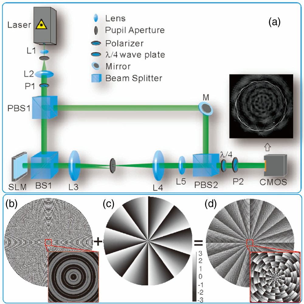
Perfect optical vortices (POVs) provide a solution to address the challenge induced by strong dependence of classical optical vortices on their carried topological charges. However, traditional POVs are all shaped into bright rings with a single main lobe along the radial direction. Here we propose a method for enhanced control on the ring profile (the radial intensity profile of circular rings) of POVs based on modulated circular sine/cosine radial functions, which is realized by a circular Dammann grating embedded with a spiral phase. Specifically, a type of “absolute” dark POVs surrounded by two bright lobe rings in each side is presented, which provides a perfect annular potential well along those dark impulse rings for trapping low-index particles, cells, or quantum gases. In addition, several POVs with different ring profiles, including conventional POVs with bright rings, the dark POVs mentioned above, and also POVs with tunable ring profiles, are demonstrated. This work opens up new possibilities to controllably tune the ring profile of perfect vortices, and this type of generalized POVs will enrich the content of singular optics and expand the application scope of perfect vortices in a range of areas including optical manipulation, both quantum and classical optical communications, enhanced optical imaging, and also novel structured pumping lasers.
Institut National de la Recherche Scientifique–Énergie, Matériaux et Télécommunications (INRS–EMT), H5A 1K6 Montréal, Quebec, Canada
Data signals consisting of arbitrarily modulated sequences of pulses are extensively used for processing and communication applications. The spectral extent of such signals is determined by the bandwidth of the individual pulses in the sequence, which imposes a fundamental limit to the maximum amount of information that can be transmitted or processed per time period. In this work, we propose and experimentally demonstrate that the frequency spectrum occupied by a data-modulated pulse sequence can be significantly compressed to well below the individual pulse bandwidth while still maintaining the temporal duration of the pulses in the sequence and without losing any of the information carried by the signal. The proposed method involves fully reversible linear transformations of the data signal along the time and frequency domains. We demonstrate successful pulse-shape-preserving spectral compression and subsequent full waveform and information recovery of a optical pulse sequence, modulated by an arbitrary data pattern, liberating over 60% of its bandwidth. These findings should prove useful for applications in signal processing, communications, and others.
Wuhan National Laboratory for Optoelectronics & School of Optical and Electronic Information, Huazhong University of Science and Technology, Wuhan 430074, China
A thermally tuned multi-channel interference widely tunable semiconductor laser is designed and demonstrated, for the first time to our knowledge, that realizes a tuning range of more than 45 nm, side-mode suppression ratios up to 56 dB, and Lorentzian linewidth below 160 kHz. AlGaInAs multiple quantum wells (MQWs) were used to reduce linewidth, which have a lower linewidth enhancement factor compared with InGaAsP MQWs. To decrease the power consumption of micro-heaters, air gaps were fabricated below the arm phase sections. For a 75 μm long suspended thermal tuning waveguide, about 6.3 mW micro-heater tuning power is needed for a round-trip phase change. Total micro-heater tuning power required is less than 50 mW across the whole tuning range, which is lower than that of the reported thermally tuned tunable semiconductor lasers.
1 Department of Information Engineering, Università degli Studi di Padova, Via Giovanni Gradenigo 6, 35131 Padova, Italy
2 Optoelectronics Research Centre, University of Southampton, Southampton SO17 1BJ, UK
We demonstrate the possibility of post-fabrication trimming of the response of nitrogen-rich silicon nitride racetrack resonators by using an ultraviolet laser. The results revealed the possibility to efficiently tune the operating wavelength of fabricated racetrack resonators to any point within the full free spectral range. This process is much faster than similar, previously presented methods (in the order of seconds, compared to hours). This technique can also be applied to accurately trim the optical performance of any other silicon photonic device based on nitrogen-rich silicon nitride.
1 State Key Laboratory for Modern Optical Instrumentation, Center for Optical & Electromagnetic Research, College of Optical Science and Engineering, International Research Center for Advanced Photonics, Zhejiang University, Hangzhou 310058, China
2 Ningbo Research Institute, Zhejiang University, Ningbo 315100, China
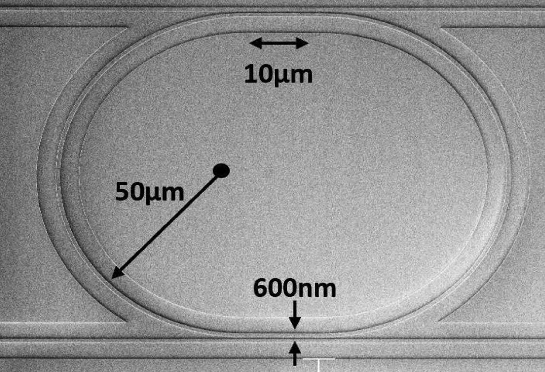
An ultrahigh-Q silicon racetrack resonator is proposed and demonstrated with uniform multimode silicon photonic waveguides. It consists of two multimode straight waveguides connected by two multimode waveguide bends (MWBs). In particular, the MWBs are based on modified Euler curves, and a bent directional coupler is used to achieve the selective mode coupling for the fundamental mode and not exciting the higher-order mode in the racetrack. In this way, the fundamental mode is excited and propagates in the multimode racetrack resonator with ultralow loss and low intermode coupling. Meanwhile, it helps achieve a compact 180° bend to make a compact resonator with a maximized free spectral range (FSR). In this paper, for the chosen 1.6 μm wide silicon photonic waveguide, the effective radius of the designed 180° bend is as small as 29 μm. The corresponding FSR is about 0.9 nm when choosing 260 μm long straight waveguides in the racetrack. The present high-Q resonator is realized with a simple standard single-etching process provided by a multiproject wafer foundry. The fabricated device, which has a measured intrinsic Q-factor as high as , is the smallest silicon resonator with a Q-factor.
Wuhan National Laboratory for Optoelectronics (WNLO) & National Engineering Laboratory for Next Generation Internet Access System, School of Optical and Electronic Information, Huazhong University of Science and Technology, Wuhan 430074, China
Distributed optical fiber Brillouin sensors detect the temperature and strain along a fiber according to the local Brillouin frequency shift (BFS), which is usually calculated by the measured Brillouin spectrum using Lorentzian curve fitting. In addition, cross-correlation, principal component analysis, and machine learning methods have been proposed for the more efficient extraction of BFS. However, existing methods only process the Brillouin spectrum individually, ignoring the correlation in the time domain, indicating that there is still room for improvement. Here, we propose and experimentally demonstrate a BFS extraction convolutional neural network (BFSCNN) to retrieve the distributed BFS directly from the measured two-dimensional data. Simulated ideal Brillouin spectra with various parameters are used to train the BFSCNN. Both the simulation and experimental results show that the extraction accuracy of the BFSCNN is better than that of the traditional curve fitting algorithm with a much shorter processing time. The BFSCNN has good universality and robustness and can effectively improve the performances of existing Brillouin sensors.
1 Key Laboratory of In-fiber Integrated Optics, Ministry of Education, Harbin Engineering University, Harbin 150001, China
2 Department of Material Chemistry, Graduate School of Engineering, Kyoto University, Nishikyo-ku, Kyoto 615-8510, Japan
3 Center of Analysis and Measurement, Harbin Institute of Technology, Harbin 150001, China
4 School of Information Engineering, Guangdong University of Technology, Guangzhou 510008, China
5 Key Laboratory of Processing and Testing Technology of Glass & Functional Ceramics of Shandong Province, School of Materials Science & Engineering, Qilu University of Technology (Shandong Academy of Sciences), Jinan 250353, China
6 e-mail: ren.jing@hrbeu.edu.cn
7 e-mail: zhangjianzhong@hrbeu.edu.cn
8 e-mail: yangj@gdut.edu.cn
Photonic media containing hybrid noble metal–dielectric nanocrystals (NCs) represent a wonderland of nanophotonics, with a myriad of uncharted optical functions yet to be explored. Capitalizing on the unique phase separation and spontaneous formation of Au-metal NCs in a gallosilicate glass, we fabricated -doped transparent nanoglass composites (GCs) containing -dielectric NCs. Compared with GCs free of Au-metal NCs, the superbroadband near-infrared emission of with a full width at half-maximum over 280 nm is enhanced twice in the dual-phase GCs. A comparison is given as to the spontaneous emission (SPE) properties of in the dual-phase GCs when pumped resonantly and off-resonantly with the localized surface plasmon resonance band of the Au-metal NCs. The important role of the Au-metal NCs in the SPE enhancement is revealed by theoretical simulation based on the finite-element method. Combining the photonic engineering effect of hybrid NCs and the sensitization effect of on , a record-high enhancement factor of over 10 of the NIR emission is achieved, and optical gain is demonstrated in the GCs at the fiber communication wavelength.
Centre for Nano Optics, University of Southern Denmark, Campusvej 55, DK-5230 Odense, Denmark
Gap-surface plasmon (GSP) metasurfaces have attracted progressively increasing attention due to their planar configurations, ease of fabrication, and unprecedented capabilities in manipulating the reflected fields that enable integrating diverse bulk-optic-based optical components into a single ultrathin flat element. In this work, we design and experimentally demonstrate multifunctional metalenses that perform simultaneous linear-polarization conversion, focusing, and beam splitting, thereby reproducing the combined functionalities of conventional half-wave plates, parabolic reflectors, and beam splitters. The fabricated single-focal metalens incorporates properly configured distinct half-wave-plate-like GSP meta-atoms and exhibits good performance under linearly polarized incidence in terms of orthogonal linear-polarization conversion () and focusing (overall ) in the wavelength spectrum ranging from 800 to 950 nm. To further extend the combined functionalities, we demonstrate a dual-focal metalens that splits and focuses a linearly polarized incident beam into two focal spots while maintaining the capability of orthogonal linear-polarization conversion. Furthermore, the power distribution between two split beams can readily be controlled by judiciously positioning the incident beam. The demonstrated multifunctional GSP-based metalenses mimic the combined functionalities of a sequence of discrete bulk optical components, thereby eliminating the need for their mutual alignment and opening new perspectives in the development of ultracompact and integrated photonic devices.
1 College of Advanced Interdisciplinary Studies, National University of Defense Technology, Changsha 410073, China
2 Hypervelocity Aerodynamics Institute, China Aerodynamics Research and Development Center, Mianyang 621000, China
3 e-mail: shandapengfei@126.com
4 e-mail: zhoupu203@163.com
High-power mode-programmable orbital angular momentum (OAM) beams have received substantial attention in recent years. They are widely used in optical communication, nonlinear frequency conversion, and laser processing. To overcome the power limitation of a single beam, coherent beam combining (CBC) of laser arrays is used. However, in specific CBC systems used to generate structured light with a complex wavefront, eliminating phase noise and realizing flexible phase modulation proved to be difficult challenges. In this paper, we propose and demonstrate a two-stage phase control method that can generate OAM beams with different topological charges from a CBC system. During the phase control process, the phase errors are preliminarily compensated by a deep-learning (DL) network, and further eliminated by an optimization algorithm. Moreover, by modulating the expected relative phase vector and cost function, all-electronic flexible programmable switching of the OAM mode is realized. Results indicate that the proposed method combines the characteristics of DL for undesired convergent phase avoidance and the advantages of the optimization algorithm for accuracy improvement, thereby ensuring the high mode purity of the generated OAM beams. This work could provide a valuable reference for future implementation of high-power, fast switchable structured light generation and manipulation.
1 Electronic Information School, Wuhan University, Wuhan 430072, China
2 NOEIC, State Key Laboratory of Optical Communication Technologies and Networks, Wuhan Research Institute of Posts and Telecommunications, Wuhan 430074, China
3 School of Physics and Technology, Center for Nanoscience and Nanotechnology, and Key Laboratory of Artificial Micro- and Nano-structures of Ministry of Education, Wuhan University, Wuhan 430072, China
4 e-mail: lizile@whu.edu.cn
5 e-mail: gxzheng@whu.edu.cn
The unwanted zero-order light accompanied by the birth of diffractive optical elements and caused mainly by fabrication errors and wavelength variations is a key factor that deteriorates the performance of diffraction-related optical devices such as holograms, gratings, beam shapers, beam splitters, optical diffusers, and diffractive microlenses. Here, inspired by the unique characteristic of nano-polarizer-based metasurfaces for both positive and negative amplitude modulation of incident light, we propose a general design paradigm to eliminate zero-order diffraction without burdening the metasurface design and fabrication. The experimentally demonstrated meta-hologram, which projects a holographic image with a wide angle of in the far field, presents a very low zero-order intensity (only 0.7% of the total energy of the reconstructed image). More importantly, the zero-order-free meta-hologram has a large tolerance limit for wavelength variations (under a broadband illumination from 520 to 660 nm), which brings important technical advances. The strategy proposed could significantly relieve the fabrication difficulty of metasurfaces and be viable for various diffractive-optics-related applications including holography, laser beam shaping, optical data storage, vortex beam generation, and so on.
1 School of Physics and Optoelectronic Engineering, Xidian University, Xi’an 710071, China
2 State Key Laboratory of Pulsed Power Laser Technology, Hefei 230037, China
3 Xi’an Research Institute of High Technology, Xi’an 710025, China
4 College of Liberal Arts and Sciences, National University of Defense Technology, Changsha 410073, China
5 e-mail: liaojiali@xidian.edu.cn
6 e-mail: xjli@nudt.edu.cn
High-order temporal soliton compression in dispersion-engineered silicon photonic crystal waveguides will play an important role in future integrated photonic circuits compatible with complementary metal–oxide–semiconductors. Here, we report the physical mechanisms of high-order temporal soliton compression affected by third-order dispersion (TOD) combined with free carrier dispersion (FCD) in a dispersion engineered silicon photonic crystal waveguide with wideband low anomalous dispersion. Through numerical temporal soliton evolution analysis, we report what we believe is the first demonstration of the dual opposite effects of TOD on temporal soliton compression, which are strengthening or weakening through two different physical mechanisms, not only depending on the sign of TOD but also the relative magnitude of TOD-induced equivalent group velocity dispersion (GVD) to the original GVD . We further find that FCD counteracts the effects of negative TOD on the soliton compression, while it reinforces the effects of positive TOD on the soliton compression. These results will help to design suitable dispersion-engineered silicon waveguides for superior on-chip temporal pulse compression in optical communications and processing application fields.
1 Department of Physics, Wesleyan University, Middletown, Connecticut 06459, USA
2 Department of Physics and Astronomy, University of Texas at San Antonio, San Antonio, Texas 78249, USA
3 Air Force Research Laboratory, Sensors Directorate, Wright-Patterson Air Force Base, Ohio 45433, USA
We propose a conceptual design of optical power limiters with abrupt limiting action and enhanced power-handling capabilities that is based on exceptional point degeneracies (EPDs). The photonic circuit consists of two coupled cavities with differential factors. One of the cavities includes a Kerr-like nonlinear material. The underlying mechanism that triggers an abrupt transmittance suppression relies on the interplay between a nonlinear instability and an abrupt destruction of EPDs due to a resonance detuning occurring when the incident power exceeds a critical value. Our proposal opens up possibilities for the use of EPDs in optical power switching, switching, routing, and so on.
1 School of Physics, University of Electronic Science and Technology of China, Chengdu 610054, China
2 Southwest Institute of Technical Physics, Chengdu 610041, China
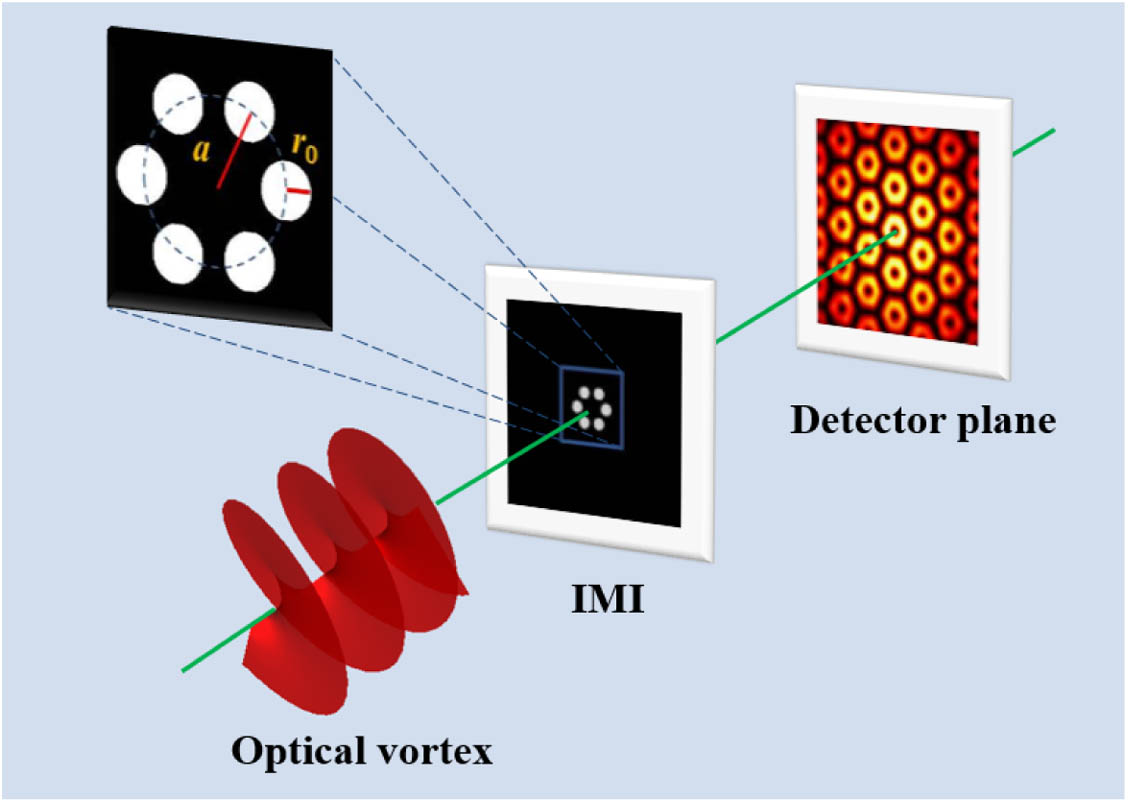
A multipoint interferometer (MI), uniformly distributed point-like pinholes in a circle, was proposed to measure the orbital angular momentum (OAM) of vortex beams [Phys. Rev. Lett.101, 100801 (2008)PRLTAO0031-900710.1103/PhysRevLett.101.100801], which can be used for measuring OAM of light from astronomical sources. This is a simple and robust method; however, it is noted that this method is only available for low topological charge because the diffracted intensity patterns for vortex beams with higher OAM will repeat periodically. Here, we propose an improved multipoint interferometer (IMI) for measuring the OAM of an optical vortex with high topological charge. The structure of our IMI is almost the same as the MI, but the size of each pinhole is larger than a point in the MI. Such a small change enables each pinhole to get more phase information from the incident beams; accordingly, the IMI can distinguish any vortex beams with different OAM. We demonstrate its viability both theoretically and experimentally.
1 Department of Electronic and Computer Engineering, Hong Kong University of Science and Technology, Clear Water Bay, Kowloon, Hong Kong, China
2 Department of Physics, Hong Kong University of Science and Technology, Clear Water Bay, Kowloon, Hong Kong, China
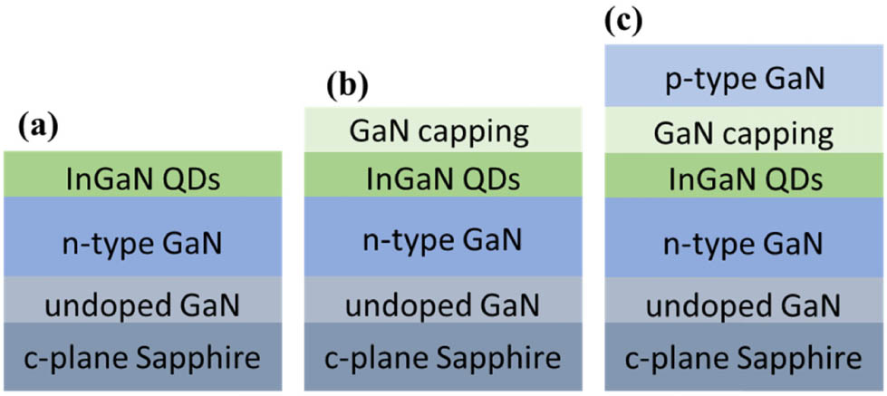
Gallium nitride (GaN)-based light-emitting diodes (LEDs) are important for lighting and display applications. In this paper, we demonstrate green-emission (512 nm) InGaN quantum dot (QD) LEDs grown on a c-plane sapphire substrate by metal-organic chemical vapor deposition. A radiative lifetime of 707 ps for the uniform InGaN self-assembled QDs is obtained by time-resolved photoluminescence measurement at 18 K. The screening of the built-in fields in the QDs effectively improves the performance of QD LEDs. These high quantum efficiency and high temperature stability green QD LEDs are able to operate with negligible efficiency droop and with current density up to . Our results show that InGaN QDs may be a viable option as the active medium for stable LEDs.
1 Key Laboratory of Semiconductor Materials Science, Institute of Semiconductors, Chinese Academy of Sciences, Beijing 100083, China
2 Center of Materials Science and Optoelectronics Engineering, University of Chinese Academy of Sciences, Beijing 100049, China
3 School of Physics and Astronomy, Cardiff University, Cardiff, UK
4 e-mail: XieS1@cardiff.ac.uk
5 e-mail: wqma@semi.ac.cn
We report on a high-performance mid-wavelength infrared avalanche photodetector (APD) with separate absorption and multiplication regions. InAs is used as the absorber material and high-bandgap is used as the multiplication material. At room temperature, the APD’s peak response wavelength is 3.27 μm, and the 50% cutoff wavelength is 3.5 μm. The avalanche gain reaches 13.1 and the responsivity is 8.09 A/W at 3.27 μm when the applied reverse bias voltage is 14.6 V. The measured peak detectivity of the device is at 3.27 μm.


 Download:1192次