1 Guangdong Provincial Key Laboratory of Optical Fiber Sensing and Communications, Institute of Photonics Technology, Jinan University, Guangzhou 510632, China
2 College of Electronic Science and Technology, Shenzhen University, Shenzhen 518060, China
3 e-mail: xiangpingli@jnu.edu.cn
4 e-mail: gpwang@szu.edu.cn
This publisher’s note reports the revision of authors’ name spelling in Photon. Res.6, 443 (2018)2327-912510.1364/PRJ.6.000443.
1 School of Optical and Electrical Information, Huazhong University of Science and Technology, Wuhan 430074, China
2 Wuhan National Laboratory for Optoelectronics, Huazhong University of Science and Technology, Wuhan 430074, China
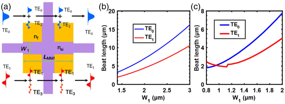
We propose and experimentally demonstrate a novel ultracompact dual-mode waveguide crossing based on subwavelength multimode-interference couplers for a densely integrated on-chip mode-division multiplexing system. By engineering the lateral-cladding material index and manipulating phase profiles of light at the nanoscale using an improved inverse design method, a subwavelength structure could theoretically realize the identical beat length for both TE0 and TE1, which can reduce the scale of the device greatly. The fabricated device occupied a footprint of only 4.8μm×4.8μm. The measured insertion losses and crosstalks were less than 0.6 dB and 24dB from 1530 nm to 1590 nm for both TE0 and TE1 modes, respectively. Furthermore, our scheme could also be expanded to design waveguide crossings that support more modes.
1 Shenzhen Key Laboratory of Advanced Thin Films and Applications, College of Physics and Energy, Shenzhen University, Shenzhen 518060, China
2 School of Physics and the Centre for Research on Adaptive Nanostructures and Nanodevices (CRANN), Trinity College Dublin, Dublin 2, Ireland
3 Key Laboratory of Materials for High-Power Laser, Shanghai Institute of Optics and Fine Mechanics, Chinese Academy of Sciences, Shanghai 201800, China
4 e-mail: wangkangpeng@msn.com
5 e-mail: luojt@szu.edu.cn
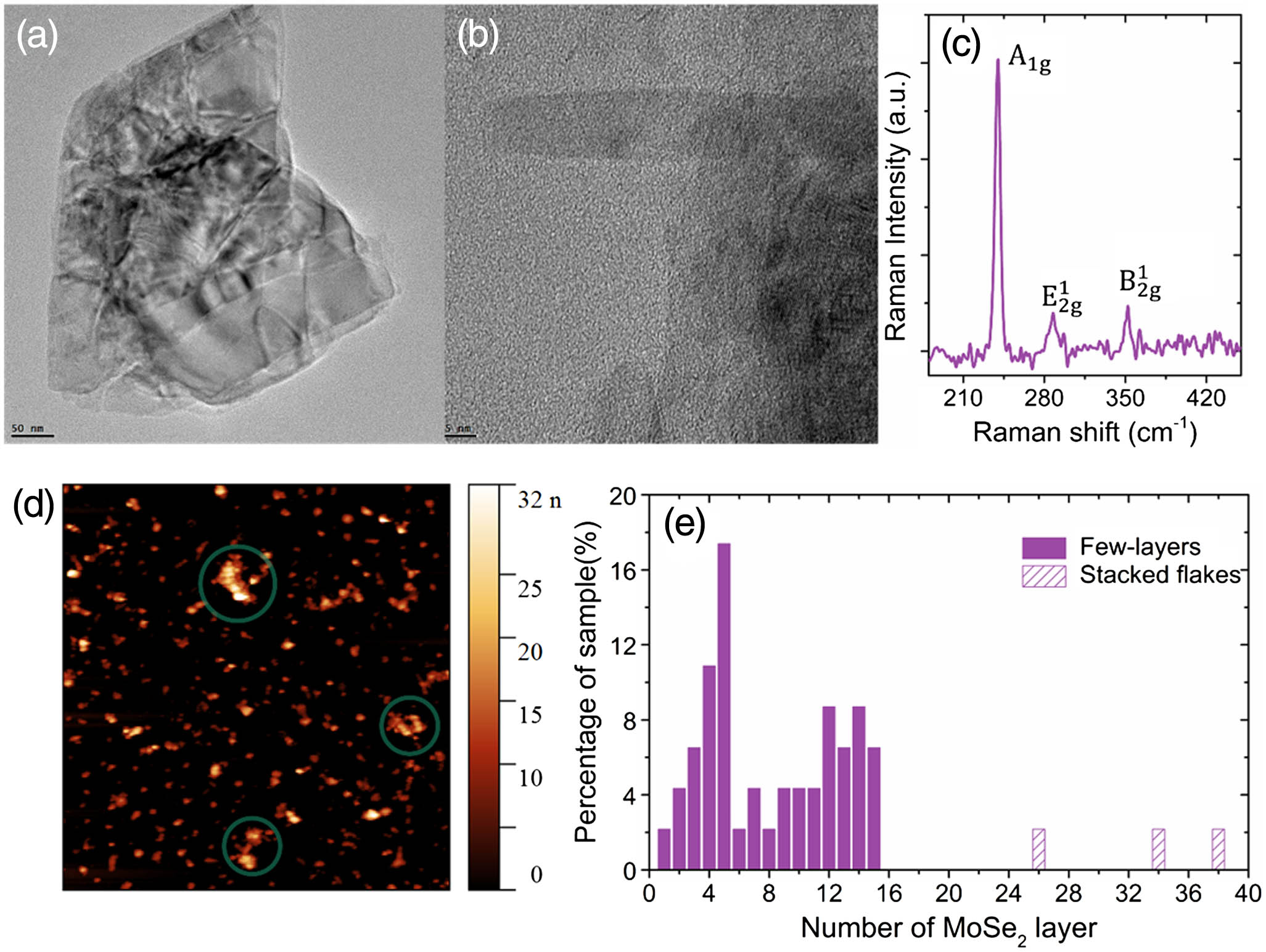
Two-dimensional transition metal dichalcogenides are considered promising materials for next-generation photonics and nano-optical devices. Although many previous reports have shown saturable absorption of molybdenum diselenide (MoSe2), these nonlinear optical (NLO) properties of MoSe2 were measured in separate works and under different conditions with their hot-carrier relaxations. Here, we conducted a series of coherent studies on the NLO properties of few-layer MoSe2 via open-aperture Z-scan and degenerate pump-probe techniques. These measurements were taken to test the materials’ capabilities as a slow-saturable absorber. A slow-absorber model was employed to analyze the NLO measurements, and the results show that the NLO modulation depth was modeled to be 7.4% and 15.1% for the linear absorption coefficients of 5.22cm1 and 6.51cm1, respectively. The corresponding saturated intensities were modeled to be 39.37MW/cm2 and 234.75MW/cm2, respectively. The excitation carrier recovery time of few-layer MoSe2 was measured by degenerate pump-probe techniques to be ~220ps. These nonlinear optical performances make it a promising slow-saturable absorber for passive mode locking in femtosecond lasers.
1 Key Laboratory of Quantum Information, University of Science and Technology of China, Chinese Academy of Sciences, Hefei 230026, China
2 College of Information Engineering, Zhejiang University of Technology, Hangzhou 310023, China
3 Synergetic Innovation Center of Quantum Information and Quantum Physics, University of Science and Technology of China, Hefei 230026, China
The dissipative sensing based on a self-interference microring resonator composed of a microring resonator and a U-shaped feedback waveguide is demonstrated experimentally. Instead of a frequency shift induced by the phase shift of the waveguide or the microcavity, the dissipative sensing converts the phase shift to the effective external coupling rate, which leads to the change of linewidth of the optical resonance and the extinction ratio in the transmission spectrum. In our experiment, the power dissipated from a microheater on the feedback waveguide is detected by the dissipative sensing mechanism, and the sensitivity of our device can achieve 0.22 dB/mW. This dissipative sensing mechanism provides another promising candidate for microcavity sensing applications.
1 Wuhan National Laboratory for Optoelectronics, Huazhong University of Science and Technology, Wuhan 430074, China
2 e-mail: huangqz@mail.hust.edu.cn
3 e-mail: jsxia@hust.edu.cn
We have designed and realized an athermal 4-channel wavelength (de-)multiplexer in silicon nitride (SiN). Minimized thermal sensitivity is achieved in a wide wavelength range by using wide and narrow waveguides with low and different thermal-optic coefficients in the two arms of Mach–Zehnder interferometers (MZIs). The SiN core layer and SiO2 cladding layers are deposited by a low-temperature plasma-enhanced chemical vapor deposition process. The fabricated MZI filter exhibits a thermal sensitivity within ±2.0pm/°C in a wavelength range of 55 nm to near 1300 nm. Then, an athermal (de-)multiplexer based on cascaded MZIs has been demonstrated with a crosstalk ≤22dB and a thermal sensitivity <4.8pm/°C for all four channels, reduced by 77% compared to a conventional SiN (de-)multiplexer. Owing to the passive operation and compatibility with the CMOS backend process, our devices have potential applications in 3D integration of photonics and electronics.
Key Laboratory for Micro-Nano Optoelectronic Devices of Ministry of Education, School of Physics and Electronics, Hunan University, Changsha 410082, China
Near-field coupled plasmonic systems generally achieve plasmonically induced transparency (PIT) using only one-way bright–dark mode coupling. However, it is challenging to realize such well-designed devices, mainly because they depend significantly on the polarization direction. We exploit surface plasmons supported by two crossed layers of graphene nanoribbons (GNRs) to achieve dynamically tunable PIT, where each GNR operates as both the bright and dark modes simultaneously. The proposed PIT can result from either one-way bright–dark mode interactions or bidirectional bright–bright and bright–dark mode hybridized coupling when the polarization is perpendicular/parallel or at an angle to the GNRs, respectively. Additionally, identical ribbon widths yield polarization-insensitive single-window PIT, whereas different ribbon widths produce polarization-dependent double-window PIT. We examine the proposed technique using plasmon wave functions and the transfer matrix method; analytical and numerical results show excellent agreement. This study can provide physical insight into the PIT coupling mechanisms and advance the applicability and versatility of PIT-based sensing platforms and other active devices.
1 Beijing Engineering Research Center for Mixed Reality and Advanced Display, School of Optics and Photonics, Beijing Institute of Technology, Beijing 100081, China
2 Beijing Key Laboratory for Metamaterials and Devices, Key Laboratory of Terahertz Optoelectronics, Ministry of Education, and Beijing Advanced Innovation Center for Imaging Technology, Department of Physics, Capital Normal University, Beijing 100048, China
3 Micro and Nanotechnology Research Center, School of Physics, Beijing Institute of Technology, Beijing 100081, China
4 e-mail: yzhang@mail.cnu.edu.cn
Metasurfaces have become a new photonic structure for providing potential applications to develop integrated devices with small thickness, because they can introduce an abrupt phase change by arrays of scatterers. To be applied more widely, active metasurface devices are highly desired. Here, a tunable terahertz meta-lens whose focal length is able to be electrically tuned by ~4.45λ is demonstrated experimentally. The lens consists of a metallic metasurface and a monolayer graphene. Due to the dependence of the abrupt phase change of the metasurface on the graphene chemical potential, which can be modulated using an applied gate voltage, the focal length is changed from 10.46 to 12.24 mm when the gate voltage increases from 0 to 2.0 V. Experimental results are in good agreement with the theoretical hypothesis. This type of electrically controlled meta-lens could widen the application of terahertz technology.
1 State Key Laboratory of Optoelectronic Materials and Technologies, School of Materials, Sun Yat-sen University, Guangzhou 510275, China
2 Key Laboratory of Materials Physics, Institute of Solid State Physics, Chinese Academy of Sciences, Hefei 230031, China
The so-called “phase difference” is commonly introduced as a phenomenological parameter in Raman tensor theory, so as to fit the experimental data well. Although phase difference is widely recognized as an intrinsic property of crystals, its physics still remains ambiguous. Recently, Kranert et al. have presented a new formalism to explain the origin of phase difference theoretically. Here, we systematically conducted experimental research with polar phonons in wurtzite crystals, the results of which strongly suggest that the phase difference should be predetermined in a Raman tensor, rather than be treated as Raman tensor elements traditionally or as an intrinsic property. On the grounds of pinpointing existing logical flaws in Raman tensor study, we provide a logically clear paradigm.
Key Laboratory for Physical Electronics and Devices of the Ministry of Education & Shaanxi Key Laboratory of Information Photonic Technique, Xi’an Jiaotong University, Xi’an 710049, China
We study the parametric amplification of electromagnetically induced transparency-assisted Rydberg six- and eight-wave mixing signals through a cascaded nonlinear optical process in a hot rubidium atomic ensemble both theoretically and experimentally. The shift of the resonant frequency (induced by the Rydberg–Rydberg interaction) of parametrically amplified six-wave mixing signal is observed. Moreover, the interplays between the dressing effects and Rydberg–Rydberg interactions in parametrically amplified multiwave mixing signals are investigated. The linear amplification of Rydberg multiwave mixing processes with multichannel nature acts against the suppression caused by Rydberg–Rydberg interaction and dressing effect.
1 Key Laboratory of Semiconductor Materials Science, Institute of Semiconductors, Chinese Academy of Sciences, Beijing 100083, China
2 Beijing Key Laboratory of Low Dimensional Semiconductor Materials and Devices, Beijing 100083, China
3 College of Materials Science and Opto-Electronic Technology, University of Chinese Academy of Sciences, Beijing 101408, China
4 e-mail: zhuoning@semi.ac.cn
A multi-wavelength sampled Bragg grating (SBG) quantum cascade laser array operating between 7.32 and 7.85 μm is reported. The sampling grating structure, which can be analyzed as a conventional grating multiplied by a sampling function, is fabricated by holographic exposure combined with optical photolithography. The sampling grating period was varied from 8 to 32 μm, and different sampling order (1st, 2nd, and 3rd order) modes were achieved. We propose that higher-order modes with optimized duty cycles can be used to take full advantage of the gain curve and improve the wavelength coverage of the SBG array, which will be beneficial to many applications.
1 Institute for Microelectronics and Microsystems, Unit of Naples, National Council of Research, Via Pietro Castellino, 80131 Naples, Italy
2 Institute of Protein Biochemistry, National Council of Research, Via Pietro Castellino, 80131 Naples, Italy
3 Lawrence Berkeley National Laboratory, Molecular Foundry Division, 67 Cyclotron Road, Berkeley, California 94720, USA
The realization of an efficient optical sensor based on a photonic crystal metasurface supporting bound states in the continuum is reported. Liquids with different refractive indices, ranging from 1.4000 to 1.4480, are infiltrated in a microfluidic chamber bonded to the sensing dielectric metasurface. A bulk liquid sensitivity of 178 nm/RIU is achieved, while a Q-factor of about 2000 gives a sensor figure of merit up to 445 in air at both visible and infrared excitations. Furthermore, the detection of ultralow-molecular-weight (186 Da) molecules is demonstrated with a record resonance shift of 6 nm per less than a 1 nm thick single molecular layer. The system exploits a normal-to-the-surface optical launching scheme, with excellent interrogation stability and demonstrates alignment-free performances, overcoming the limits of standard photonic crystals and plasmonic resonant configurations.
1 Electrical and Computer Engineering, University of California—Davis, Davis, California 95618, USA
2 W&WSens Devices, Inc., 4546 El Camino, Suite 215, Los Altos, California 94022, USA
3 Electrical Engineering, Baskin School of Engineering, University of California, Santa Cruz, California 95064, USA
4 e-mail: sislam@ucdavis.edu
In this paper, high-speed surface-illuminated Ge-on-Si pin photodiodes with improved efficiency are demonstrated. With photon-trapping microhole features, the external quantum efficiency (EQE) of the Ge-on-Si pin diode is >80% at 1300 nm and 73% at 1550 nm with an intrinsic Ge layer of only 2 μm thickness, showing much improvement compared to one without microholes. More than threefold EQE improvement is also observed at longer wavelengths beyond 1550 nm. These results make the microhole-enabled Ge-on-Si photodiodes promising to cover both the existing C and L bands, as well as a new data transmission window (1620–1700 nm), which can be used to enhance the capacity of conventional standard single-mode fiber cables. These photodiodes have potential for many applications, such as inter-/intra-datacenters, passive optical networks, metro and long-haul dense wavelength division multiplexing systems, eye-safe lidar systems, and quantum communications. The CMOS and BiCMOS monolithic integration compatibility of this work is also attractive for Ge CMOS, near-infrared sensing, and communication integration.
1 Nanophotonics Research Centre, Shenzhen Key Laboratory of Micro-Scale Optical Information Technology, Shenzhen University, Shenzhen 518060, China
2 Department of Electronic Engineering, Jinan University, Guangzhou 510632, China
3 Department of Physics, Capital Normal University, Beijing Key Laboratory of Metamaterials and Devices, Key Laboratory of Terahertz Optoelectronics, Ministry of Education, and Beijing Advanced Innovation Center for Imaging Technology, Beijing 100048, China
4 State Key Laboratory of Optoelectronic Materials and Technologies and School of Electronics and Information Technology, Sun Yat-sen University, Guangzhou 510275, China
5 e-mail: leiting@szu.edu.cn
6 e-mail: li_zhaohui@hotmail.com
The quickly increasing data transfer load requires an urgent revolution in current optical communication. Orbital angular momentum (OAM) multiplexing is a potential candidate with its ability to considerably enhance the capacity of communication. However, the lack of a compact, efficient, and integrated OAM (de)multiplexer prevents it from being widely applied. By attaching vortex gratings onto the facets of a few-mode fiber, we demonstrate an integrated fiber-based OAM (de)multiplexer. A vortex grating fabricated on the fiber facet enables the direct multiplexing of OAM states at one port and the demultiplexing of OAM states at the other port. The measured bit error rate of the carrier signal after propagating through a 5-km few-mode fiber confirms the validity and effectiveness of the proposed approach. The scheme offers advantages in future high-capacity OAM communication based on optical fiber.
1 School of Materials and Energy, Guangdong University of Technology, Guangzhou 510006, China
2 Department of Applied Physics, The Hong Kong Polytechnic University, Hung Hom, Kowloon, Hong Kong, China
3 Laboratory of All-Solid-State Light Sources, Institute of Semiconductors, Chinese Academy of Sciences, Beijing 100083, China
4 e-mail: zhangling@semi.ac.cn
5 e-mail: yuen.tsang@polyu.edu.hk
The novel vertically standing PtSe2 film on transparent quartz was prepared by selenization of platinum film deposited by the magnetron sputtering method, and an Nd:LuVO4 passively mode-locked solid-state laser was realized by using the fabricated PtSe2 film as a saturable absorber. The X-ray diffraction pattern and Raman spectrum of the film indicate its good crystallinity with a layered structure. The thickness of PtSe2 film is measured to be 24 nm according to the cross-section height profile of the atomic force microscope image. High-resolution transmission electron microscopy images clearly demonstrate its vertically standing structure with an interlayer distance of 0.54 nm along the c-axis direction. The modulation depth (ΔT) and saturation fluence (s) of PtSe2 film are measured to be 12.6% and 17.1μJ/cm2, respectively. The obtained mode-locked laser spectrum has a central wavelength of 1066.573 nm, with a 3 dB bandwidth of 0.106 nm. The transform limited pulse width of the mode-locked laser was calculated to be 15.8 ps. A maximum average output power of 180 mW with a working repetition rate of 61.3 MHz is obtained. To the best of our knowledge, this is the first report of the generation of ultrafast mode-locked laser pulses by using layered PtSe2 as a saturable absorber.
1 MOE Key Laboratory of Material Physics and Chemistry under Extraordinary Conditions, and Shaanxi Key Laboratory of Optical Information Technology, School of Science, Northwestern Polytechnical University, Xi’an 710129, China
2 Department of Public Education, Northwestern Polytechnical University Ming De College, Xi’an 710124, China
3 e-mail: pengli@nwpu.edu.cn
4 e-mail: jlzhao@nwpu.edu.cn
Polarization oscillating beams, namely, polarization standing waves, commonly formed by a pair of coherent counterpropagating light waves with orthogonal polarizations, oscillate their states of polarization periodically within a wavelength interval, offering conceptual and practical interests in light-matter interactions such as the nonreciprocal magnetoelectric effect, and impressive applications in optical imaging, sensing, and chirality detection. Here, we propose a new class of polarization oscillating beams that longitudinally vary states of polarization with spatial intervals within centimeters via the superposition of two copropagating optical frozen waves with preshaped longitudinal intensity profiles and transverse phase structures. The flexibility and manipulability are demonstrated by creating several polarization oscillating beams with different polarization structures. This work paves a new way to manipulate other waves and may be useful for applications of optical standing waves in optical manipulation, light guiding of atoms, polarization-sensitive sensing, etc.


 Download:773次