红外与毫米波学报, 2024, 43 (1): 63, 网络出版: 2023-12-26  

MBE脱氧条件与InGaAs/InP APD性能的相关性【增强内容出版】

Correlation between MBE deoxidation conditions and InGaAs/InP APD performance
作者单位
1 中国科学院上海技术物理研究所 红外物理国家重点实验室,上海 200083
2 中国科学院大学,北京 100049
3 上海科技大学 物质科学与技术学院,上海 201210
4 上海量子科学研究中心,上海 201315
5 复旦大学 应用表面物理国家重点实验室和物理学系,上海 200438
摘要
InP基InGaAs/InP雪崩光电二极管(APD)对近红外光具有高敏感度,使其成为微弱信号和单光子探测的理想光电器件。然而随着先进器件结构越来越复杂,厚度尺寸从量子点到几微米不等,性能越来越受材料中晶格缺陷的影响和工艺条件的制约。采用固态源分子束外延(MBE)技术分别在As和P气氛保护下对InP衬底进行脱氧处理并外延生长晶格匹配的In0.53Ga0.47As薄膜和APD结构材料。实验结果表明,As脱氧在MBE材料质量方面比P脱氧具有明显的优势,可获得陡直明锐的异质结界面,降低载流子浓度,提高霍尔迁移率,延长少子寿命,并抑制器件中点缺陷或杂质缺陷引起的暗电流。因此,As脱氧可以有效提高MBE材料的质量,这项工作优化了InP衬底InGaAs/InP外延生长参数和器件制造条件。
Abstract
InP-based InGaAs/InP avalanche photodiodes (APDs) have high sensitivity to near-infrared light, making them ideal optoelectronic devices for weak signal and single-photon detection. However, as device structures become complex and advanced, with thickness and sizes ranging from quantum dots to several micrometers, performance is increasingly constrained by defects in the lattice of the material and the process conditions. Solid source molecular beam epitaxy (MBE) technology was used to deoxidize InP substrates under the atmosphere As and P, respectively, and epitaxially grow lattice-matched In0.53Ga0.47As film and InGaAs/InP avalanche APD full-structure materials. The experiment results demonstrate that As deoxidation has a distinct advantage over P deoxygenation in terms of MBE material quality, which can make a straight and sharp heterojunction interface, lower carrier concentrations, higher Hall mobilities, longer minority carrier lifetimes, and achieve suppression of dark current caused by point defects or impurity defects in the device. Therefore, As deoxidation can be applied effectively to enhance the quality of MBE materials. This work optimizes InP substrate InGaAs/InP epitaxial growth parameters and device fabrication conditions.

1 Introduction

The III-V semiconductor material InGaAs has a direct band gap and high optical absorption efficiency in the near-infrared band,which can be matched with the lattice of InP materials with good collisional ionization properties as one of the replaceable indirect band gap silicon-based materials1. Avalanche photodiodes(APDs)fabricated of InP and InGaAs materials for quantum key distribution2,deep-space communications3,3-D light detection and ranging45,etc.,have many advantages such as high performance,high reliability,and low cost making a promising development outlook as optical signal detector applications. However,the performance of APDs is often limited by lattice defects in InP and InGaAs materials and the process conditions as the improvement of the structures. Therefore,preparing high-performance InGaAs/InP APD material remains challenging for researchers.

Molecular beam epitaxy(MBE)technology which has become more advanced in recent years,can control the parameters in the material deposition process,such as temperaturegas flow rate,sputtering,and deoxidation conditions,and precisely control the material thickness at the atomic layer scale,thus effectively regulating the material crystal structure and properties such as mobilitydark current and light saturation current67. In the MBE process,the atmosphere of evaporative sources is used to remove natural oxides from the substrate surface and protect against As evaporation damage,thus avoiding pollution from oxygen and other gases,known as deoxidation protection89. However,the effects of deoxidation atmospheres such as As and P sources on the performance of materials and devices,like impurities at arsenic-phosphorus heterojunctions,still need further research and optimization.1011.

In this paper,InP substrates were deoxidized under the atmosphere protection of As4 and P2,respectively. An ultra-high vacuum solid source molecular beam epitaxy(MBE)system grew lattice-matched In0.53Ga0.47As film and APD full-structure materials. The material minority carrier lifetimes were characterized by time-resolved photoluminescence(TRPL). The variation of As and P atoms and impurity concentration with thickness at the material structure interface were gauged by SIMS. The fluctuation of the In0.53Ga0.47As/InP heterojunction interface and necessary geometrical information is observed by scanning transmission electron microscopy(STEM). Finally,planar APD devices were prepared,and the IV characteristics were measured.

The effect of As-source deoxidation conditions is superior to that of P-source deoxidation conditions in terms of material surface morphology,lattice quality,minority carrier lifetime,and dark device current. This work offers a practical foundation for identifying optimal epitaxial growth and device processing parameters for InP-based InGaAs/InP.

1 Experiments

1.1 Material growth

The left side of Figure 1 shows the InGaAs/InP APD device structure cross-section,and the right shows the electric field distribution. To evaluate the effect of different deoxidation atmosphere conditions of As4 and P2 on the APD device performance,we grew high-quality InGaAs/InP APD epitaxial materials on AXT(100)InP substrates using the MBE(DCA P600)system. A three-temperature valve-controlled solid-state phosphorus cracking source and a two-temperature valve-controlled arsenic cracking furnace were used as the group V sources,and conventional Knudsen cells for Gallium and Indium are used as the group III source.
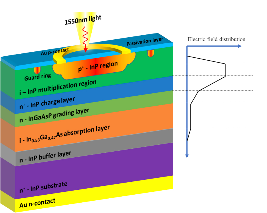
图 1. InGaAs/InP APD结构的剖面图和内部电场分布

Fig. 1. Profile diagram and internal electric field distribution of InGaAs/InP APD structure

下载图片 查看所有图片

The InP substrate was first put into the load lock and baked at 200°C to remove the adsorbed water vapor and then degassed in a pretreatment chamber at 300°C for 20 min. In the growth chamber,the intensity of the beam flux of each source at different temperatures was corrected to determine the growth temperature of each source. The beam flux ratios of group V and group III elements were determined using the beam flux monitors(BFM). The substrate was then transferred to the growth chamber. The substrate temperature of sample A was elevated under the protection of the As4 atmosphere,and sample B was performed under the P2 atmosphere to desorb the oxides from the surface. A clear 2×4 reconstitution stripe appeared on the reflection high-energy electron diffraction(RHEED)fluorescence screen,indicating desorption of the oxide layer on the substrate surface9. Afterward,the sample holder temperature continued to be raised by 30°C(thermocouple temperature ~640°C)and maintained for 6-7 min to allow complete desorption of the oxide film and flattening of the atomic layer on the substrate surface. After cooling down to the growth temperature,the beam equivalent pressure(BEP)ratios of each beam source furnace were controlled by valves to epitaxially grow 1~2 μm lattice-matched unintentionally doped In0.53Ga0.47As/InP film materials,and APD structured wafers. The APD material was based on a separate absorption,grading,charge,and multiplication(SAGCM)structure,including an n-InP buffer layer,an intrinsic In0.53Ga0.47As absorber layer,an InGaAsP component gradient layer,an n-type highly doped InP charge control layer,intrinsic InP cap layer,divides into Sample A(As4 deoxygenated)and Sample B(P2 deoxygenated)4.

1.2 Material characterization

After growth,the materials were characterized using XRD to determine the component values and the lattice quality. Van der Pauw method Hall test(Ecopia HMS-3000)was performed to characterize the carrier transport properties of epitaxial In0.53Ga0.47As/InP materials of different thicknesses.

TRPL can characterize the direct electron-hole recombination(band-to-band recombination),Shockley-Read-Hall(SRH)recombination,and other non-radiative recombination information of materials absorbing pulsed laser radiation. 12. The time-correlated single-photon counting(TCSPC)is a crucial technique for fluorescence lifetime imaging due to its high signal-to-noise ratio and high temporal resolution13. The dynamics of carrier recombination in APD structure materials were studied using the TCSPC method with a 1064 nm laser,and the results were compared with samples from the anti-reflective coating(ARC)SiNx passivation treatment(front-end process)14. The single-photon detector is a Hamamatsu H10330C -75 microchannel plate detector with a time resolution of 20 ps.

The SIMS principle is to use a focused ion beam sputtering the surface of semiconductors and then use a time-of-flight or mass spectrometer to analyze the secondary ions formed in the sputtering process,which allows for high-precision detection of the elemental distribution and interface impurities in the film materials from nanometer to tens of microns in depth1516. We used the SIMS(Cameca IMF 5F,Evans Analytical Group)test to observe the high-precision measurement of different elemental concentrations in structural samples to analyze and determine the growth behavior and quality of InGaAs lattice epitaxy on InP substrates. The detection limit(DL) is over 1.0×10¹⁰ to 1×10¹⁶ atoms/cm-3.

Interfaces and defects in MBE-grown InGaAs/InP films were further examined using aberration-corrected STEM. Cross sections of STEM sample A(As4 deoxygenated)and sample B(P2 deoxygenated)were prepared using the focused ion beam(FIB)technique(Helios-G4-CX,Thermo Fisher Scientific). The STEM investigations were performed with a field-emission STEM(Themis Z,Thermo Fisher Scientific)fit with a probe and an image aberration corrector(SCORR and CETCOR,CEOS GmbH). The microscope was operated at 300 kV. For HAADF-STEM imaging,the probe semi-convergent angle was set to 21.4 mrad,and the semi-collection angle of the detector was arranged from 76 to 200 mrad. The STEM images were collected with[101]zone axis.

1.3 Device preparation and characterization

After characterization,the incident surfaces of APD materials were coated with SiNx ARC to eliminate reflections from the air-InP interface. The wafers were fabricated into 20 µm diameter planar InGaAs/InP APD by front-end processes such as Zn doping and UV lithography,including Device A(As4 deoxygenated)and Device B(P2 deoxygenated)1117. The IV characteristics were measured by a semiconductor parameter analyzer(Keysight 4200)at room temperature.

2 Results and discussions

2.1 Hall effect analysis

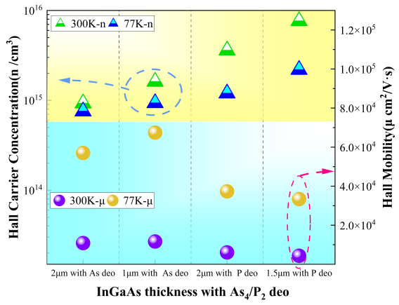
Figure 2 shows the carrier concentration n and Hall mobility μ of epitaxially grown unintentionally doped In0.53Ga0.47As/InP films under different deoxidation atmospheres at 330K and 77K. Four samples exhibit lower carrier concentrations at 77K than 300K. In contrast,μvalues at 77K are higher than that at 300K,with mobility even exceeding 6.0×104 cm2/Vs. This is due to the decreased lattice vibration scattering caused by low temperaturesµphononT-3/2),fewer impurity scattering noises from the In0.53Ga0.47As intrinsic growth(µlatticeT3/2),and lower transport energy of the thermally activated carriers. Thus,the In0.53Ga0.47As/InP materials with As4 protective atmosphere possess superior carrier transport capability than those with P2 deoxidation protection,with higher mobility and lower carrier concentration. This suggests that As4 deoxidation can help reduce impurity contamination and associated point defects introduced by the growth process.

图 2. 霍尔载流子浓度和迁移率图

Fig. 2. Hall carrier concentration and mobility plot

下载图片 查看所有图片

2.2 TRPL analysis

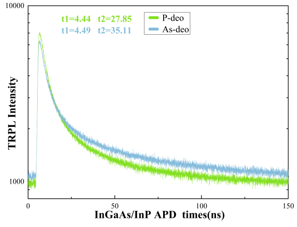
Figure 3 shows the time instrumental response function(IRF)fluorescence decay curves generated and extracted under a single laser pulse for the TRPL test. For the APD structured wafer,the 1064 nm light pulse is mainly absorbed by the InGaAs layer,and the minority carrier lifetime is reflected in the InGaAs layer. It is generally believed that the InP cap layer has little impact on the absorption layer of the 1064 nm light10. The double exponential fit(ExpDec2)using the nonlinear least squares inverse convolution method is set to obtain the minority carrier lifetimes t1 and t2,which generally correspond to the SRH recombination t1shorter lifetime)and radiation recombination t2longer lifetime)of the InP charge layer or InGaAs layer of the APD materials. Although the model presents several limitations and drawbacks,it is accepted due to its simplicity 18.

图 3. APD晶圆的TRPL光谱

Fig. 3. TRPL spectra of APD wafers

下载图片 查看所有图片

The smoother the decay of the measured TRPL curve,the larger the τ value,indicating the stability of wafer quality. The smaller the variation of the τ value,the better the wafer quality. We can see that As4 deoxidation has a longer minority carrier lifetime t2 than P2 deoxidation,indicating that the wafer of As4 deoxidation is of better quality than that of P2 deoxidation,with relatively fewer lattice defects and impurities and less radiation recombination. The t1 of the samples is tiny,which indicates that the carriers in the wafer are rapidly quenched after capture,with strong non-radiative recombination,and there may be many deep energy level recombination with high doping concentrations or background concentrations.

2.3 SIMS analysis
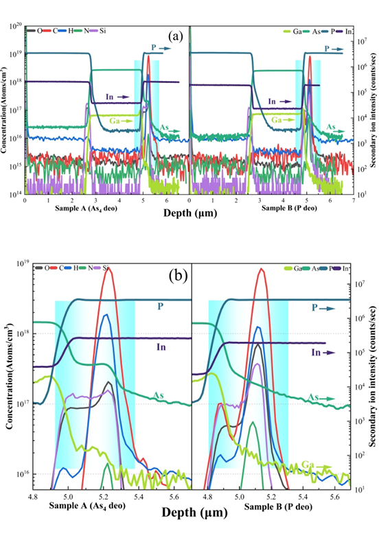
Figure 4(a)shows the depth distribution of Ga,As,P,In(right axis)and O,C,H,N,Si(left axis)in the MBE-grown InGaAs/InP APD wafers. The near-surface trailing in the SIMS profiles,especially for C,O,and H,can be explained by the kick-on of the impurity atoms from the surface contaminations into the depth by the primary ion beam and no more than 20-50 nm19. Different deoxidation conditions do not distinctly affect the concentrations of Ga and P,As,and In of sample A(As4 deoxidation)and sample B(P2 deoxidation). However,O and Si impurities increased when switching the valve sources for GaAs and InP growth(d = 2-3μm,d = 4.8-5.6μm). C and H content increase significantly at deoxidation(d = 4.8-5.6μm). In Figure 4(b),the increase in O content at d = 4.8-5.6μm is more significant for sample B than sample A. This tailing could represent impurity concentration in the matrix,or it may be caused by impurity segregation at grain boundaries and dislocations and secondary implantation of the surface contaminants. Therefore,we perform a retest to avoid the interference caused by the surface contaminants. Table 1 summarizes the peak results of the two SIMS tests for C,O,N,H,and Si impurities,with no change in the data values. However,sample B has an O concentration nearly an order of magnitude higher than A,despite being close to the detection limit. This implies that P2 deoxidation during MBE may have more negative effects than As4 deoxidation,which may cause impurity accumulation on the rough surface,lattice,and interfacial dislocations of the material19.

图 4. (a)通过 As4、P2 脱氧样品的SIMS深度分布对比,(b)深度d = 4.8-5.6 μm的脱氧界面对比

Fig. 4. (a) Comparison of SIMS depth distributions for Samples via As4, P2 deoxidation,(b) Bulk regions (d = 4.8-5.6 μm) of comparison of deoxidation interface

下载图片 查看所有图片

表 1. SIMS测量的(d = 4.8-5.6μm)的区域杂质平均最大浓度(cm-3)

Table 1. Average peak concentrations (cm-3 ) of impurities in bulk regions (d = 4.8-5.6 μm) from SIMS measurements.

SampleOCHSiN
A2.25E+179.76E+182.08E+181.56E+171.86E+16
B8E+179.09E+181.34E+183.74E+176.61E+16
DL1E151E151E161E145E14

查看所有表

2.4 STEM analysis

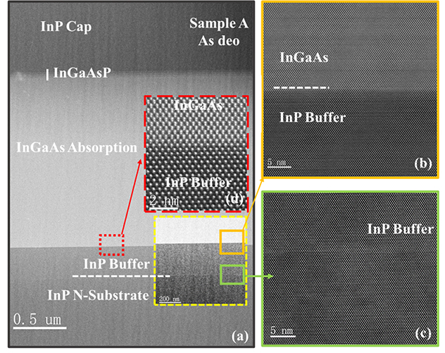
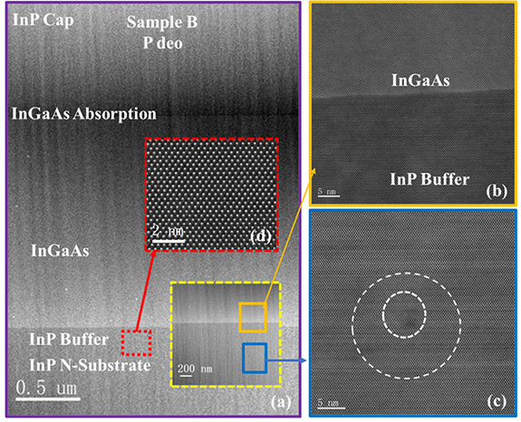
Figure 5-6 shows the HAADF-STEM images of the epitaxial cross-sectional structure of sample A(As4 deoxidation)and sample B(P2 deoxidation). According to the Z-contrast imaging mechanism of HAADF-STEM,the elements of Ga,and As shown brighter contrast than P atoms,giving InP,InGaAsP,and InGaAs their distinct differences in atomic resolved images20. Figures 5(a)and 6(a)show the wafer epitaxial cross-sectional structure. Figures 5(b)and 6(b)show a detailed scan of the InP buffer layer and InGaAs absorber layer heterojunction interface. Figures 5(c)and 6(c)show the InP buffer and substrate homojunction interface. Sample A clearly shows the sharp and straight interface between InGaAs and InP buffer layer and InP substrate,which is atomically smooth. Sample B shows only a slightly floating heterogeneous interface. And the homogeneous interface could not be characterized with grayscale fluctuations. Stacked layer dislocations or lattice distortions may lead to interface roughness2021. This indicates that sample A has a more explicit interface and better interfacial quality than sample B.

图 5. APD 样品A的STEM-HAADF图像(As-脱氧)(a)FIB网格上的APD结构图像,(b)InGaAs和InP缓冲层的图像,(c)InP同质结界面的区域,(d)(a)中红框区域的高分辨率图像

Fig. 5. STEM-HAADF image of APD sample A(As-deoxidation)(a)an image of the APD structure on FIB grid,(b)the image of InGaAs and InP buffer,(c)zoom region of InP homojunction interfaces,(d)high-resolution images of the region marked with a red frame in(a)

下载图片 查看所有图片

As shown in Fig. 5(d)and Fig. 6(d),the InGaAs layer appears as dumbbells at the atomic-scale resolution,InP appear as single dots,and the interfacial atomic layers are regularly arranged22. It indicates that the initial growth of MBE under As4 deoxidation conditions is controlled precisely,and the InP buffer layer can be stably controlled at the atomic scale. However,the unevenness of the heterogeneous interfaces of Sample B causes some heterojunctions to be identified in atomic resolution hardly. Therefore,the As4 deoxidation process avoids more defects and improves the lattice quality. This may be because As atoms are more challenging to stay on the substrate surface than P atoms. Sufficient or excess As4 sources can ensure adequate absorption of impurities such as oxygen of the substrate surface by reducing the In-O bonding on the surface while avoiding the metallization of the As atoms on the InAs surface by desorption23-25.

图 6. APD样品B的STEM-HAADF图像(P-脱氧)(a)FIB网格上的APD结构图像,(b)InGaAs和InP缓冲层的图像,(c)InP同质结界面的区域和堆叠缺陷(圆圈)圆圈表示具有不同核心结构的位错,(d)(a)中红框区域的高分辨率图像

Fig. 6. STEM-HAADF image of APD sample B(P-deoxidation)(a)an image of the APD structure on the FIB grid,(b)the image of InGaAs and InP buffer,(c)the zoom region of InP homojunction interfaces and stacking fault(circled). Circles indicate dislocations with different core structures,(d)high-resolution images of the area marked with a red frame in(a)

下载图片 查看所有图片

2.5 Device IV analysis

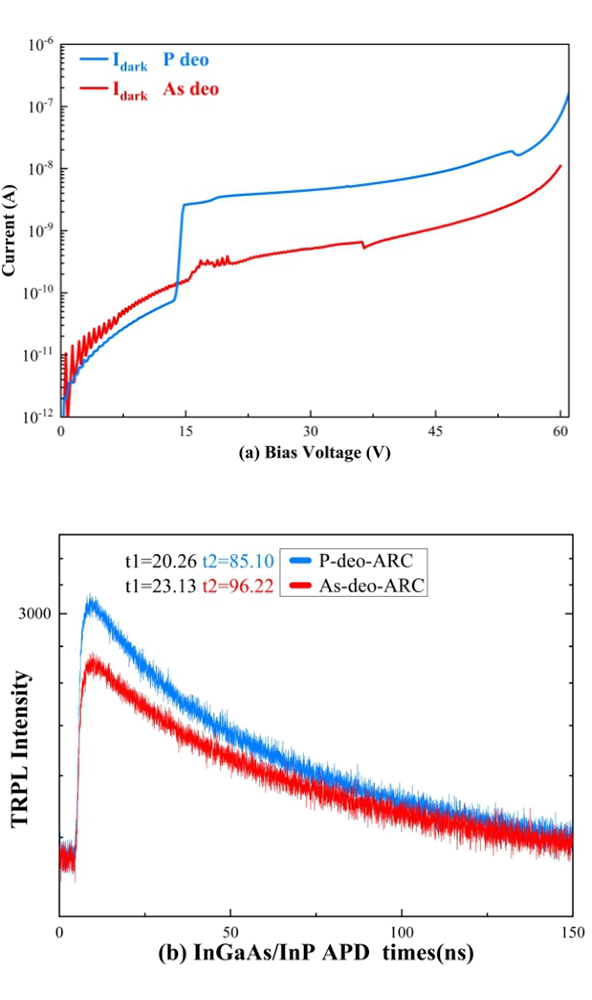
Figure 7(a)shows the current-voltage IV)characteristics of InGaAs/InP APD Device A(As4 deoxidation)and Device B(P2 deoxidation)operating in linear mode. Based on the collisional ionization principle of phonon scattering,the hot carriers in the InP collide with the lattice to generate dark current and zero photocurrents at lower reverse bias voltages. When the APD reaches the punch through voltage (near 15 V),the depletion region extends to the InGaAs absorption region. When the reverse bias voltage is between 15V and 60V,electrons move toward the substrate and holes toward the InGaAsP grading layer and the InP multiplication layer. At the same time,the number of carriers in collisional ionization increases until the breakdown voltage(near 60 V)is reached,the current is wholly transferred to the multiplication layer,and the APD enters the Geiger mode from the linear mode26-28. The main components of dark current include the generation-recombination current,tunneling current,and leakage current. Generation-recombination current is affected by carrier concentrations,minority carrier effective lifetime τeff and temperature. Tunneling current is mainly affected by band gap and trap energy levels. Higher carrier mobility and a longer lifetime can usually reduce the dark current of the device. Considering that surface leakage and weak external natural light interference have little effect on device applications,we ignore the differences in the dark current below the punch-through voltage1129.

图 7. (a)InGaAs/InP APD的I-V曲线,(b)经钝化处理的APD材料TRPL光谱

Fig. 7. (a) I-V and gain characteristics of the InGaAs/InP APD,(b) TRPL spectra of ARC-APD

下载图片 查看所有图片

Compared to device A(As4 deoxidation),device B(P2 deoxidation)has a lower punch-through voltage,a slightly higher breakdown voltage,and a more extended linear region(less than 1 V). This is mainly due to the small thickness difference of the InP multiplication layer2830. The elevated bias voltage increases the tunneling current in the absorption layer,which can lead to a significant increase in the dark current,thus affecting the performance and power consumption of the device. We note that near the punch-through voltagethe dark current of device B is 2.62×10⁻⁹ A,an order of magnitude larger than the dark current of device A of 1.62×10⁻¹⁰ A. From figure 2the carrier concentration of the InGaAs layer with As4 deoxidation is lower,thus resulting in a lower dark current at the punch-through voltage. Meanwhile,the higher carrier mobility of InGaAs layers implies fewer intrinsic defects in the As4 deoxidation materials. Therefore,the generation-recombination current caused by defects is relatively small.

The carrier lifetime measured for wafers is not the bulk carrier lifetime τb but rather the effective lifetime τeffτb,including surface and bulk recombination. When the surface layer of the wafer is coated with SiNx passivation,it can reduce the surface recombination and reflection loss,enhance the absorption of light,and suppress the surface leakage,which makes τeff closer to τb3132. Figure 7(b)shows the TRPL curves of APD wafers after ARC. Both t1 and t2 increase significantly,and the effective lifetime with As4 deoxidation τeff is longer than that with P2 deoxidation. This indicates that ARC has improved the performance of APD,but As4 deoxidation still maintains better performance than P2 deoxidation.

Combined the IV analysis with the above Hall test and TRPL results,the APD with As4 deoxidation has lower carrier concentrations,higher Hall mobilities,and higher minority carrier lifetimes compared to the P2 deoxidation,which produces some suppression of the dark current caused by point defects or impurity defect energy levels. The SIMS and STEM results also support this view further.

3 Conclusions

In summary,we used the MBE technique to deoxidize InP substrates under As4 and P2 atmosphere protection and grow In0.53Ga0.47As/InP epitaxial layer APD structures. The material quality is evaluated by STEM,TRPL,Hall test,SIMS,and other characterization methods. The APD devices were prepared by a front-end process. The IV characteristics were measured at room temperature. The effects of MBE deoxidation conditions on the material surface morphology,lattice quality,minority carrier lifetime,and dark device current were analyzed. The results show that compared with P2 deoxidation,As4 deoxidation can significantly improve the MBE material quality,make the heterogeneous interface structure stable and sharp,improve theHall mobility,reduce thecarrier concentration,lengthen the minority carrier lifetime,and have a specific suppression effect on the device dark current caused by point defects or impurity defects. This study provides valuable information on InP/InGaAs APD material devices prepared by MBE.

参考文献

[1] 李雪, 龚海梅, 邵秀梅, 等. 短波红外InGaAs焦平面研究进展[J]. 红外与毫米波学报, 2022, 41(1): 129-138.

    LI Xue, GONG Hai-Mei, SHAO Xiu-Mei, et al. Recent advances in short wavelength infrared InGaAs focal plane arrays[J]. J. Infrared Millim. Waves, 2022, 41(1): 129-138.

[2] NAMEKATA N, MAKINO Y, INOUE S. Single-photon detector for long-distance fiber-optic quantum key distribution[J]. Optics Letters, 2002, 27(11): 954-6.

[3] MENDENHALL J A, CANDELL L M, HOPMAN P I, et al. Design of an Optical Photon Counting Array Receiver System for Deep-Space Communications[J]. Proceedings of the IEEE, 2007, 95(10): 2059-69.

[4] JIANGX, WILTONS, KUDRYASHOVI, et al. InGaAsP/InP Geiger-mode APD-based LiDAR [M]. Optical Sensing, Imaging, and Photon Counting: From X-Rays to THz. 2018. 10.1117/12.2322757

[5] LEWISJ S, LEOG, BROWNG J, et al. Development of an InGaAs SPAD 2D array for flash LIDAR [M]. Quantum Sensing and Nano Electronics and Photonics XV. 2018. 10.1117/12.2289270

[6] PANISH M B. Molecular Beam Epitaxy of GaAs and InP with Gas Sources for As and P[J]. Journal of The Electrochemical Society, 1980, 127(12): 2729-33.

[7] 杨瑛, 王红真, 范柳燕、, 等. 分子束外延高铟组分InGaAs薄膜研究[J]. 红外与毫米波学报, 2022, 41(6): 987-994.

    YANG Ying, WANG Hong-Zhen, FAN Liu-Yan, et al. Study on Molecular Beam Epitaxy of High indium InGaAs Films[J]. J. Infrared Millim. Waves, 2022, 41(6): 987-994.

[8] BASTIMAN F, CULLIS A G. GaAs(001) planarization after conventional oxide removal utilising self-governed InAs QD site selection[J]. Applied Surface Science, 2010, 256(13): 4269-71.

[9] KHAIREH-WALIEH A, ARNOULT A, PLISSARD S, et al. Monitoring MBE Substrate Deoxidation via RHEED Image-Sequence Analysis by Deep Learning[J]. Crystal Growth & Design, 2023, 23(2): 892-8.

[10] ZHANG Y, GU Y, ZHENG W, et al. Anomalous arsenic diffusion at InGaAs/InP interface[J]. Materials Research Express, 2018, 6(3).

[11] GUO Z, WANG W, LI Y, et al. Material Defects and Dark Currents in InGaAs/InP Avalanche Photodiode Devices[J]. IEEE Transactions on Electron Devices, 2022: 1-6.

[12] AHRENKIEL R K, ELLINGSON R, JOHNSTON S, et al. Recombination lifetime of In0.53Ga0.47As as a function of doping density[J]. Appl Phys Lett, 1998, 72(26): 3470-2.

[13] XIAO D, SAPERMSAP N, SAFAR M, et al. On Synthetic Instrument Response Functions of Time-Correlated Single-Photon Counting Based Fluorescence Lifetime Imaging Analysis[J]. Frontiers in Physics, 2021: 9.

[14] ROSFJORD K M, YANG J K W, DAULER E A, et al. Nanowire Single-photon detector with an integrated optical cavity and anti-reflection coating[J]. Opt Express, 2006, 14(2): 527-34.

[15] EBNESAJJADS. Chapter 4 - Surface and Material Characterization Techniques [M]//EBNESAJJAD S. Surface Treatment of Materials for Adhesive Bonding (Second Edition). Oxford; William Andrew Publishing. 2014: 39-75. 10.1016/b978-0-323-26435-8.00004-6

[16] IYENGAR V V, NAYAK B K, GUPTA M C. Silicon PV devices based on a single step for doping, anti-reflection and surface passivation[J]. Solar Energy Materials and Solar Cells, 2010, 94(12): 2205-11.

[17] WEN J, WANG W J, CHEN X R, et al. Origin of large dark current increase in InGaAs/InP avalanche photodiode[J]. Journal of Applied Physics, 2018, 123(16).

[18] PéAN E V, DIMITROV S, DE CASTRO C S, et al. Interpreting time-resolved photoluminescence of perovskite materials[J]. Physical Chemistry Chemical Physics, 2020, 22(48): 28345-58.

[19] RESHCHIKOV M A, VOROBIOV M, ANDRIEIEV O, et al. Determination of the concentration of impurities in GaN from photoluminescence and secondary-ion mass spectrometry[J]. Scientific Reports, 2020, 10(1): 2223.

[20] SMITH D J. Atomic-resolution structure imaging of defects and interfaces in compound semiconductors[J]. Progress in Crystal Growth and Characterization of Materials, 2020, 66(4): 100498.

[21] PAULAUSKAS T, BUURMA C, COLEGROVE E, et al. Atomic scale study of polar Lomer–Cottrell and Hirth lock dislocation cores in CdTe[J]. Acta Crystallographica Section A, 2014, 70(6): 524-31.

[22] CHU M W, LIOU S C, CHANG C P, et al. Emergent Chemical Mapping at Atomic-Column Resolution by Energy-Dispersive X-Ray Spectroscopy in an Aberration-Corrected Electron Microscope[J]. Physical Review Letters, 2010, 104(19): 196101.

[23] SCHäFER M, NAUMANN W, FINNBERG T, et al. UV/ozone-activated growth of oxide layers on InAs(001) surfaces and oxide desorption under arsenic pressure[J]. Applied Surface Science, 2000, 158(1): 147-58.

[24] ZHOU X, LUO Z-J, GUO X, et al. Surface segregation of InGaAs films by the evolution of reflection high-energy electron diffraction patterns[J]. Chinese Physics B, 2012, 21(4).

[25] NAOKI KOBAYASHI N K, YASUYUKI KOBAYASHI Y K. As and P Desorption from III-V Semiconductor Surface in Metalorganic Chemical Vapor Deposition Studied by Surface Photo-Absorption[J]. Japanese Journal of Applied Physics, 1991, 30(10A): L1699.

[26] ZENG Q Y, WANG W J, WEN J, et al. Dependence of dark current on carrier lifetime for InGaAs/InP avalanche photodiodes[J]. Optical and Quantum Electronics, 2015, 47(7): 1671-7.

[27] MOHAMMADNEJAD S, AGHAEI F. Noise characteristics improvement of submicron InP/InGaAs avalanche photodiode for laser detection system[J]. Opt Commun, 2020: 455124561.

[28] LI K, DUAN X, LIU K, et al. High-speed and low dark current InGaAs/InAlAs avalanche photodiodes with P-type absorption layers[J]. Optical and Quantum Electronics, 2023, 55(5): 422.

[29] ZENG Q Y, WANG W J, WEN J, et al. Effect of surface charge on the dark current of InGaAs/InP avalanche photodiodes[J]. Journal of Applied Physics, 2014, 115(16): 164512.

[30] XU J, CHEN X, WANG W, et al. Extracting dark current components and characteristics parameters for InGaAs/InP avalanche photodiodes[J]. Infrared Physics & Technology, 2016: 76(468-73.

[31] SCHMIDT J, ABERLE A G. Easy-to-use surface passivation technique for bulk carrier lifetime measurements on silicon wafers[J]. Progress in Photovoltaics: Research and Applications, 1998, 6(4): 259-63.

[32] POLLOCK K L, JUNGE J, HAHN G. Detailed Investigation of Surface Passivation Methods for Lifetime Measurements on P-Type Silicon Wafers[J]. IEEE Journal of Photovoltaics, 2012, 2(1): 1-6.

郭子路, 王文娟, 曲会丹, 范柳燕, 诸毅诚, 王亚杰, 郑长林, 王兴军, 陈平平, 陆卫. MBE脱氧条件与InGaAs/InP APD性能的相关性[J]. 红外与毫米波学报, 2024, 43(1): 63. Zi-Lu GUO, Wen-Juan WANG, Hui-Dan QU, Liu--Yan FAN, Yi-Cheng ZHU, Ya-Jie WANG, Chang-Lin ZHENG, Xing-Jun WANG, Ping-Ping CHEN, Wei LU. Correlation between MBE deoxidation conditions and InGaAs/InP APD performance[J]. Journal of Infrared and Millimeter Waves, 2024, 43(1): 63.

引用该论文: TXT   |   EndNote

相关论文

加载中...

关于本站 Cookie 的使用提示

中国光学期刊网使用基于 cookie 的技术来更好地为您提供各项服务,点击此处了解我们的隐私策略。 如您需继续使用本网站,请您授权我们使用本地 cookie 来保存部分信息。
全站搜索
您最值得信赖的光电行业旗舰网络服务平台!