Opto-Electronic Advances, 2018, 1 (6): 180010, Published Online: Mar. 19, 2019  

Mode evolution and nanofocusing of grating-coupled surface plasmon polaritons on metallic tip

Author Affiliations
1 MOE Key Laboratory of Material Physics and Chemistry under Extraordinary Conditions and Shaanxi Key Laboratory of Optical Information Technology, School of Science, Northwestern Polytechnical University, Xi'an 710072, China
2 Key Laboratory of Optoelectronic Technology and Systems (Ministry of Education), Chongqing University, Chongqing 400044, China
3 MOE Key Laboratory of Weak-Light Nonlinear Photonics, TEDA Applied Physics Institute and School of Physics, Nankai University, Tianjin 300457, China
Abstract
We present a detailed analysis on mode evolution of grating-coupled surface plasmonic polaritons (SPPs) on a conical metal tip based on the guided-wave theory. The eigenvalue equations for SPPs modes are discussed, revealing that cylindrical metal waveguides only support TM01 and HEm1 surface modes. During propagation on the metal tip, the grating-coupled SPPs are converted to HE31, HE21, HE11 and TM01 successively, and these modes are sequentially cut off except TM01. The TM01 mode further propagates with drastically increasing effective mode index and is converted to localized surface plasmons (LSPs) at the tip apex, which is responsible for plasmonic nanofocusing. The gap-mode plasmons can be excited with the focusing TM01 mode by approaching a metal substrate to the tip apex, resulting in further enhanced electric field and reduced size of the plasmonic focus.

1 Introduction

Plasmonic nanofoucsing techniques have received increasing attentions for concentrating light energy into a nanoscale spatial region1. In consequence, the electric field can be significantly enhanced with mode volume maintained in nanoscale. Such an excellent characteristic has been exploited in a wide range of applications in tip-enhanced Raman spectroscopy (TERS)2-4, surface enhanced Raman spectroscopy (SERS) 5-8, nonlinear optics9-13, and super-resolution imaging14, 15, etc. The key to achieving plasmonic nanofocusing is the design of metal nanostructures with excellent localized surface plasmon resonance (LSPR) effect, such as wedges16, tetrahedrons17, grooves18, nanoparticles19, etc. Besides, it is noteworthy that noble metallic tips can combine electric field enhancement and spatial confinement characteristics to generate nano-confined light source20, 21.

Conical metal tips have been commonly adopted for TERS in the configuration of scanning probe microscopy22. Conical metal tips are typically fabricated by electrochemically etching gold/silver wires23, and directly illuminated at the tip apex with a focused laser beam24. Localized surface plasmons (LSPs) are excited at the tip apex to enhance the near field as the nano-confined light source. Subject to the diffraction limit, however, the focus light spot under the far-field illumination is much larger than the size of the enhanced near field, and thus background signal excitation is inevitable, which in turn limits sensing performance in some circumstances22.

An effective way to avoid the background signal excitation is based on a conical metal tip with grating-assisted light coupling25-27, which has also been exploited in the fields of grating-assisted SPP interferences28, imaging29, lithography30, etc. In this scheme, a diffractive grating is fabricated on the metal tip body at a distance of tens of microns from the tip apex to achieve momentum matching between the far-field excitation light and the surface plasmonic polaritons (SPPs)31-33. The grating-coupled SPPs propagate along the metal body and are finally converted to LSPs confined at the tip apex. Although such a scheme has been applied in nano-Raman/nonlinear spectroscopy34, 35, the mechanism of plasmonic mode evolution and the resulting nanofocusing has not been clearly understood36-39.

In this paper, we present a detailed analysis on mode evolution of grating-coupled SPPs on the conical metal tip based on the guided-wave theory. The eigenvalue equations of guided SPP modes and mode fields of allowed eigenmodes are examined for cylindrical plasmonic guides. The propagation of the grating-coupled SPPs on the conical metal tip is numerical simulated by using the finite difference time domain (FDTD) solution software (Lumerical Inc.), revealing plasmonic mode evolution for realization of nanofocusing.

2 Results and discussion

As an excellent plasmonic material in the visible band, silver is selected for the metal tip model, as illustrated in Fig. 1. As a proof of principle, the dielectric constant of silver is selected as εAg=-18.281+0.48108i at the excitation wavelength λ=632.8 nm40. In addition, the dielectric constant of silver given by other model can also be used in our calculations41. A slit grating with a period of $ \mathit{\Lambda} $ =1180 nm, a slit width of 20 nm and a depth of 50 nm is fabricated onto the shaft of the silver tip at a distance of L=12 μm from the tip apex. The included angle between the excitation light and the surface normal of the tip body is q. The curvature radius at the apex and the conical angle of the tip are r=20 nm and α=10°, respectively.
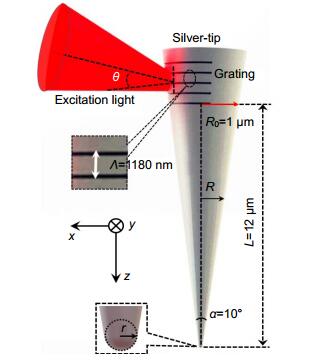
Fig. 1. Geometry of a conical silver tip with grating-assisted light coupling.The excitation light is focused onto the diffractive grating. R is the cross-sectional radius of the tip body gradually decreasing from 1 μm to 20 nm. The tip apex is modeled as a hemisphere with a radius of r.

下载图片 查看所有图片

Under the condition of k0R0≫1 42, where k0 is the wave vector of the far-field excitation light, and R0 is the cross-sectional radius of the tip body at the location of the grating, a diffractive grating located on a flat silver film as sketched in Fig. 2(a) can be taken as an approximation to the case given in Fig. 1, since the diameter of the silver tip is much greater than the wavelength of the grating-coupled SPPs. In addition, according to the propagation characteristic of SPPs43, 44, the tip model may be considered as an assembly of a planar grating structure that excites SPPs and a conical plasmonic tip that transmits and focuses the SPPs. The role of the planar grating is to match the wave vectors of the far-field excitation light and the SPP mode. The SPPs can be excited under the phase-matching condition ${k_{{\rm{SPP}}}} = {k_{//}} + {k_{\rm{G}}} $25, with the wave vector of SPPs ${k_{{\rm{SPP}}}}{\rm{ = Re}}({n^{{\rm{SPP}}}})2{\rm{ \mathsf{ π} }}/\lambda $, the wave vector component of the excitation light parallel to the surface of planar grating ${k_{//}} = 2{\rm{ \mathsf{ π} }}\sin \theta /\lambda $, and the grating vector ${k_{\rm{G}}}{\rm{ = }}2{\rm{ \mathsf{ π} }}\ell /\Lambda $. $ \ell $ and $\mathit{\Lambda} $ are the diffraction order and the period of the grating, respectively. The effective index of the SPPs can be written as $ n_{{\rm{eff}}}^{{\rm{SPP}}} = {[{\varepsilon _{{\rm{Ag}}}}{\varepsilon _{\rm{d}}}/({\varepsilon _{{\rm{Ag}}}} + {\varepsilon _{\rm{d}}})]^{1/2}}$42, i.e. neff =1.0285, where εd=1 is the surrounding's dielectric constant. Confined by the limited width of the grating structure, the grating-coupling SPPs for the model shown in Fig. 1 should have lower effective index than this value. The phase-matching condition gives θ=30° for $\ell {\rm{ = }}1 $, as shown in Fig. 2(b). In agreement with the analytical calculation, the simulation result shown in Fig. 2(c) presents a reflection minimum at θ=28.5° for λ=632.8 nm. In the simulation, the focused Gaussian beam is approximated with a plane wave. Here, the total field scattered field (TFSF) is used to prevent the possible coupling with the boundaries of the simulation area. The polarization of the excitation field is parallel to the incident plane. In Fig. 2(d), the corresponding Re(Hy) distribution illustrates the generation and propagation of SPPs at the silver-air interface.

Fig. 2. (a) Sketch map of SPPs excitation using a planar grating; (b) Dispersion relationship of SPPs and the grating coupling; (c) Reflection obtained from the field monitor located above the surface without grating; (d) Re(Hy) distribution of the grating-coupled SPPs generation and propagation along the silver-air interface with excitation wavelength at λ=632.8 nm and θ=28.5°.

下载图片 查看所有图片

To understand the guided SPP modes in an adiabatic tapered plasmonic waveguide, the effective indices (neff) of the SPP guided modes are determined by the corresponding eigenvalue equations in a cylindrical metal waveguide with varying radius, which are derived from the Maxwell's equations with boundary conditions at the metal-air interface. The eigenvalue equation for the TM01 mode is written as45, 46

where Km(x) is the modified Bessel function, and Im(x) is the modified Hankel function, ${\chi _1} = {(\beta _{}^2 - {\varepsilon _{{\rm{Ag}}}}{\omega ^2}/{c^2})^{1/2}} $, $ {\chi _2} = {(\beta _{}^2 - {\varepsilon _{\rm{d}}}{\omega ^2}/{c^2})^{1/2}}$, and β is the propagation constant. Similarly, the eigenvalue equation of the HEmn mode can also be derived (Supplementary information Section 1).

where

For a certain m, there are multiple solutions by solving Eq. (2). Since the radial field distribution has only one maximum at the metal-air interface of the silver tip, the radial number can only take n=1. Due to the p-polarization nature of SPPs, the cylindrical waveguide supports TM01 mode with radial polarization distribution but forbids the TE01 mode owing to its azimuthal polarization characteristic47. In addition, there is no solution of EHmn modes on the silver-air interface48.

According to Eqs. (1) and (2), we can calculate the effective indices of the cylindrical silver waveguide with a radius of R, shown as the solid curves in Figs. 3(a) and 3(b), which are in excellent agreement with the simulation results plotted in dotted curves by using the MODE solution software (Lumerical Inc.). Figures 3(d-j) show the transverse mode field intensity distributions simulated at R=1 μm. As seen in Fig. 3(a), multiple SPP guided modes, including TM01, $ {\rm{HE}}_{11}^{x/y}$, ${\rm{HE}}_{21}^{{\rm{e/o}}} $ and $ {\rm{HE}}_{31}^{{\rm{e/o}}}$, can exist in the surface of plasmonic guide for large radius, but the high-order SPP guided modes have effective indices reaching unity and thus are gradually cut off as the radius decreases, i.e. at R=815 nm, 440 nm, and 60 nm for ${\rm{HE}}_{31}^{{\rm{e/o}}} $, ${\rm{HE}}_{21}^{{\rm{e/o}}} $ and ${\rm{HE}}_{11}^{x/y} $, respectively. In contrast, TM01 mode will never be cut off with decreasing R and has effective mode index approaching infinity.

Fig. 3. Effective indices neff in real part (a) and imaginary part (b) of guided SPP modes versus the radius of cylindrical silver guide R. (c) Sketch map of a silver tip removing the diffracting grating. (d–j) Transverse modes intensity distributions of guided modes for R=1 μm.

下载图片 查看所有图片

For the assembly of the diffraction grating and the metallic tip illustrated in Fig. 1 under far-field excitation, Figure 4 shows the evolutionary process of the plasmonic mode field ending up with nanofocusing. Figure 4(a) is the transverse mode intensity distribution of the grating-coupled SPPs under the condition of k0R0≫1. In Fig. 3(a), it can be seen that the effective refractive neff of the grating-coupled SPPs denoted by the pink line is close to that of the HE31 mode for R≈1000 nm, so part of the grating-coupled SPPs are firstly coupled to the HE31 mode, as shown in Fig. 4(b). With R gradually decreasing to less than 800 nm, the HE31 mode is cut off, and only with a short evanescent tail in the propagation direction, as depicted in Fig. 4(c). At the same time, the neff of grating-coupled SPPs is gradually close to that of the HE21 mode, so part of them is further coupled to the HE21 mode, as shown in Fig. 4(d), and the HE21 mode can propagate along the interface of the tip. At R=440 nm, the HE21 mode is also cut off. Only the remaining grating-coupled SPPs propagate along the surface of the tip, as shown in Fig. 4(e). With further reduction of the tip radius, the grating-coupled SPPs is partly coupled to HE11 mode at R=130 nm due to the phase mismatch coupling, as shown in Fig. 4(f). After the HE11 mode is cut off at R=60 nm, only the TM01 mode evolved by grating-coupled SPPs propagates along the interface in accompany with a small amount of remaining grating-coupled SPPs, as shown in Fig. 4(g).

Fig. 4. (a) Transverse mode intensity distributions of the grating-coupled SPPs at R=1 μm; (b–g) Transverse mode intensity distributions of the hybrid mode at R=800, 750, 600, 350, 230, and 20 nm, respectively. (h) Electric field intensity distribution at the tip apex. (i) Transverse electric field intensity distribution at 1 nm below the tip apex.

下载图片 查看所有图片

In order to ensure that the TM01 mode can propagate to the tip apex with minimal non-ohmic loss, i.e. via radiation, the condition of the adiabatic parameter $\delta (R){\rm{ = }} $$ {\rm{|d}}{(k_{{\rm{T}}{{\rm{M}}_{01}}}^{{\rm{SPP}}})^{ - 1}}/{\rm{d}}R{\rm{|}}\tan (\alpha )$≪1 must be satisfied27. In other words, the conical tip angle α must be less than a critical value to allow TM01 mode to adiabatically transmit to the tip apex. On the other hand, a small α causes SPPs to experience longer transmission distance to reach the tip apex, inevitably increasing the ohmic loss. Therefore, an optimum α compromises the ohmic and the radiational losses. The competition between these two effects also leads to a wavelength-dependent conical angle for optimum energy delivery to the tip apex27, 49, 50. Considering the actual condition of the electrochemically etched silver tip, we select α=10° and r=20 nm to calculate the adiabatic parameter δ, and the corresponding calculated result is presented in Fig. 5.

Fig. 5. Adiabatic parameter δ of TM01 mode versus R.

下载图片 查看所有图片

Note that δ increases from 0.04 to 0.3 as the radius decreases from 60 nm to 20 nm. The TM01 mode thus can propagate with insignificant nonohmic loss due to satisfaction of the adiabatic approximation condition illustrated in Fig. 5, while ends up with highly localized surface plasmons as implied by its effective mode index that approaches infinity. Consequently, plasmatic nanofocusing is achieved by converting the TM01 mode propagating along the tip surface to the LSPs at the tip apex. In reality, however, the adiabatic approximation condition will gradually fail in the hemispherical part of the tip apex. Thus, while approaching the tip apex and turning to LSPs, the TM01 mode is converted to the electromagnetic radiation into free space, as shown in Fig. 4(h). This limits the focusing spot size and the location of maximum electric intensity deviates from the tip surface. Figure 4(i) is the transverse mode intensity distribution of the focal field located 1 nm below the tip apex with an electric field enhancement factor of EF=$ |{E_{{\rm{Apex}}}}/{E_{{\rm{Incident}}}}{|^2}$ =25 (where EApex and EIncident are the amplitudes of the electric field at the apex and the incident electric field, respectively), which is smaller than that obtained by direct far-field illumination on the silver tip apex, i.e EF≈ 80 (Supplementary information Section 2).

To further increase the field enhancement factor at the silver tip apex, a silver substrate is placed 2 nm below the tip apex to construct the gap mode, as shown in Fig. 6(a). The simulated field intensity distribution of the gap mode is shown in Fig. 6(b), it can be known that the gap-mode plasmons can be excited by the focusing TM01 mode, and the gap-mode intensity is effectively improved together with reduced spot size. The corresponding intensity distribution of the gap mode located 1 nm under the tip apex is depicted in Fig. 6(c). Note that the gap-mode plasmons can reach EF≈500, which is an order of magnitude higher than that of the non-gap mode and meets the requirements of TERS or nonlinear optics applications. Meanwhile, the gap mode enhances longitudinal polarization components and improves focusing capability, as illustrated in Figs. 6(b) and 6(d).

Fig. 6. (a) Gap-mode configuration with the gap distance d=2 nm. (b) Electric field intensity and polarization distributions in the x-z plane. (c) Electric field intensity distribution in the x-y plane at 1 nm below the tip apex. (d) Comparison of electric field enhancement factor between the non-gap mode (Fig. 4(i)) and gap mode located at 1 nm below the apex of the silver tip.

下载图片 查看所有图片

3 Conclusions

We present a detailed analysis on mode evolution of grating-coupled SPPs on a conical metal tip based on the guided-wave theory. The eigenvalue equation of HEmn modes for cylindrical metal waveguides is presented. During propagation on the metal tip, the grating-coupled SPPs can be gradually coupled to HE31, HE21, HE11 and TM01 modes, and these modes are sequentially cut off except TM01. The TM01 mode further propagates with drastically increasing effective mode index and thus is converted to LSPs at the tip apex, which is responsible for plasmonic nanofocusing. The gap-mode plasmons can be excited with the focusing TM01 mode by approaching a metal film to the tip apex, resulting in further enhanced electric field and reduced size of the plasmonic focus.

4 Acknowledgements

This work was financially supported by the National Natural Science Foundation of China (NSFC) (61675169, 61377055 and 11634010), the National Key R & D Program of China (2017YFA0303800), and the Fundamental Research Funds for the Central Universities (3102017zy021, 3102017HQZZ 022).

5 Competing interests

The authors declare no competing financial interests.

6 Supplementary information

Section 1: Derivation of eigenvalue equation.

Section 2: Enhancement factor of the silver tip directly illuminated by far-filed excitation light.

References

[1] D K Gramotnev, S I Bozhevolnyi. Nanofocusing of electromagnetic radiation. Nat Photonics, 2013, 8: 13-22.

[2] R M Stöckle, Y D Suh, V Deckert, R Zenobi. Nanoscale chemical analysis by tip-enhanced Raman spectroscopy. Chem Phys Lett, 2000, 318: 131-136.

[3] S Jiang, Y Zhang, R Zhang, C R Hu, M H Liao, et al.. Distinguishing adjacent molecules on a surface using plasmon-enhanced Raman scattering. Nat Nanotechnol, 2015, 10: 865-869.

[4] J H Zhong, X Jin, L Y Meng, X Wang, H S Su, et al.. Probing the electronic and catalytic properties of a bimetallic surface with 3 nm resolution. Nat Nanotechnol, 2017, 12: 132-136.

[5] J F Li, Y F Huang, Y Ding, Z L Yang, S B Li, et al.. Shell-isolated nanoparticle-enhanced Raman spectroscopy. Nature, 2010, 464: 392-395.

[6] W D Zhang, C Li, K Gao, F F Lu, M Liu, et al.. Surface-enhanced Raman spectroscopy with Au-nanoparticle substrate fabricated by using femtosecond pulse. Nanotechnology, 2018, 29: 205301.

[7] H Wei, F Hao, Y Z Huang, W Z Wang, P Nordlander, et al.. Polarization dependence of surface-enhanced Raman scattering in gold nanoparticle-nanowire systems. Nano Lett, 2008, 8: 2497-2502.

[8] K C Xu, Z Y Wang, C F Tan, N Kang, L W Chen, et al.. Uniaxially stretched flexible surface Plasmon resonance film for versatile surface enhanced Raman scattering diagnostics. ACS Appl Mater Interfaces, 2017, 9: 26341-26349.

[9] C C Neacsu, G A Reider, M B Raschke. Second-harmonic generation from nanoscopic metal tips: symmetry selection rules for single asymmetric nanostructures. Phys Rev B, 2005, 71: 201402.

[10] M Kauranen, A V Zayats. Nonlinear plasmonics. Nat Photonics, 2012, 6: 737-748.

[11] Y J Jin, L W Chen, M X Wu, X Z Lu, R Zhou, et al.. Enhanced saturable absorption of the graphene oxide film via photonic nanojets. Opt Mater Express, 2016, 6: 1114-1121.

[12] L W Chen, X R Zheng, Z R Du, B H Jia, M Gu, et al.. A frozen matrix hybrid optical nonlinear system enhanced by a particle lens. Nanoscale, 2015, 7: 14982-14988.

[13] Z R Du, L W Chen, T S Kao, M X Wu, M H Hong. Improved optical limiting performance of laser-ablation-generated metal nanoparticles due to silica-microsphere-induced local field enhancement. Beilstein J Nanotechnol, 2015, 6: 1199-1204.

[14] C Chen, N Hayazawa, S Kawata. A 1.7 nm resolution chemical analysis of carbon nanotubes by tip-enhanced Raman imaging in the ambient. Nat Commun, 2014, 5: 3312.

[15] R Zhang, Y Zhang, Z C Dong, S Jiang, C Zhang, et al.. Chemical mapping of a single molecule by plasmon-enhanced Raman scattering. Nature, 2013, 498: 82-86.

[16] K V Nerkararyan. Superfocusing of a surface polariton in a wedge-like structure. Phys Lett A, 1997, 237: 103-105.

[17] N C Lindquist, P Nagpal, A Lesuffleur, D J Norris, S H Oh. Three-dimensional plasmonic nanofocusing. Nano Lett, 2010, 10: 1369-1373.

[18] V S Volkov, S I Bozhevolnyi, S G Rodrigo, L Martín-Moreno, F J García-Vidal, et al.. Nanofocusing with channel plasmon polaritons. Nano Lett, 2009, 9: 1278-1282.

[19] A I Fernández-Domínguez, S A Maier, J B Pendry. Collection and concentration of light by touching spheres: a transformation optics approach. Phys Rev Lett, 2010, 105: 266807.

[20] E Verhagen, A Polman, L K Kuipers. Nanofocusing in laterally tapered plasmonic waveguides. Opt Express, 2008, 16: 45-57.

[21] B N Tugchin, N Janunts, A E Klein, M Steinert, S Fasold, et al.. Plasmonic tip based on excitation of radially polarized conical surface plasmon polariton for detecting longitudinal and transversal fields. ACS Photonics, 2015, 2: 1468-1475.

[22] J Stadler, T Schmid, R Zenobi. Developments in and practical guidelines for tip-enhanced Raman spectroscopy. Nanoscale, 2012, 4: 1856-1870.

[23] T X Huang, S C Huang, M H Li, Z C Zeng, X Wang, et al.. Tip-enhanced Raman spectroscopy: tip-related issues. Anal Bioanal Chem, 2015, 407: 8177-8195.

[24] P Verma. Tip-enhanced Raman spectroscopy: technique and recent advances. Chem Rev, 2017, 117: 6447-6466.

[25] C Ropers, C C Neacsu, T Elsaesser, M Albrecht, M B Raschke, et al.. Grating-coupling of surface plasmons onto metallic tips: a nanoconfined light source. Nano Lett, 2007, 7: 2784-2788.

[26] C C Neacsu, S Berweger, R L Olmon, L V Saraf, C Ropers, et al.. Near-field localization in plasmonic superfocusing: a nanoemitter on a tip. Nano Lett, 2010, 10: 592-596.

[27] S Berweger, J M Atkin, R L Olmon, M B Raschke. Light on the tip of a needle: plasmonic nanofocusing for spectroscopy on the nanoscale. J Phys Chem Lett, 2012, 3: 945-952.

[28] T Xu, C T Wang, C L Du, X G Luo. Plasmonic beam deflector. Opt Express, 2008, 16: 4753-4759.

[29] T Xu, C L Du, C T Wang, X G Luo. Subwavelength imaging by metallic slab lens with nanoslits. Appl Phys Lett, 2007, 91: 201501.

[30] X G Luo, T Ishihara. Surface plasmon resonant interference nanolithography technique. Appl Phys Lett, 2004, 84: 4780.

[31] D Sadiq, J Shirdel, J S Lee, E Selishcheva, N Park, et al.. Adiabatic nanofocusing scattering-type optical nanoscopy of individual gold nanoparticles. Nano Lett, 2011, 11: 1609-1613.

[32] M Müller, V Kravtsov, A Paarmann, M B Raschke, R Ernstorfer. Nanofocused Plasmon-driven sub-10 fs electron point source. ACS Photonics, 2016, 3: 611-619.

[33] S Schmidt, B Piglosiewicz, D Sadiq, J Shirdel, J S Lee, et al.. Adiabatic nanofocusing on ultrasmooth single-crystalline gold tapers creates a 10-nm-sized light source with few-cycle time resolution. ACS Nano, 2012, 6: 6040-6048.

[34] S Berweger, J M Atkin, R L Olmon, M B Raschke. Adiabatic Tip-Plasmon focusing for Nano-Raman spectroscopy. J Phys Chem Lett, 2010, 1: 3427-3432.

[35] V Kravtsov, J M Atkin, M B Raschke. Group delay and dispersion in adiabatic plasmonic nanofocusing. Opt Lett, 2013, 38: 1322-1324.

[36] M Esmann, S F Becker, B B da Cunha, J H Brauer, R Vogelgesang, et al.. k-space imaging of the eigenmodes of sharp gold tapers for scanning near-field optical microscopy. Beilstein J Nanotechnol, 2013, 4: 603-610.

[37] J Mihaljevic, C Hafner, A J Meixner. Grating enhanced apertureless near-field optical microscopy. Opt Express, 2015, 23: 18401-18414.

[38] J S Lee, S Han, J Shirdel, S Koo, D Sadiq, et al.. Superfocusing of electric or magnetic fields using conical metal tips: effect of mode symmetry on the plasmon excitation method. Opt Express, 2011, 19: 12342-12347.

[39] P Andrey. Nanofocusing of surface Plasmons at the apex of metallic probe tips. J Nanoelectron Optoe, 2010, 5: 310-314.

[40] P B Johnson, R W Christy. Optical constants of the noble metals. Phys Rev B, 1972, 6: 4370-4379.

[41] PalikE DHandbook of Optical Constants of Solids (Academic, San Diego, America, 1998)

[42] M I Stockman. Nanofocusing of optical energy in tapered plasmonic waveguides. Phys Rev Lett, 2004, 93: 137404.

[43] Z Y Fang, C F Lin, R M Ma, S Huang, X Zhu. Planar plasmonic focusing and optical transport using CdS nanoribbon. ACS Nano, 2010, 4: 75-82.

[44] Z Y Fang, L R Fan, C F Lin, D Zhang, A J Meixner, et al.. Plasmonic coupling of bow tie antennas with Ag nanowire. Nano Lett, 2011, 11: 1676-1680.

[45] V S Gurevich, M N Libenson. Surface polaritons propagation along micropipettes. Ultramicroscopy, 1995, 57: 277-281.

[46] A J Babadjanyan, N L Margaryan, K V Nerkararyan. Superfocusing of surface polaritons in the conical structure. J Appl Phys, 2000, 87: 3785.

[47] W D Zhang, L G Huang, K Y Wei, P Li, B Q Jiang, et al.. Cylindrical vector beam generation in fiber with mode selectivity and wavelength tunability over broadband by acoustic flexural wave. Opt Express, 2016, 24: 10376-10384.

[48] L Novotny, C Hafner. Light propagation in a cylindrical waveguide with a complex, metallic, dielectric function. Phys Rev E, 1994, 50: 4094-4106.

[49] D K Gramotnev, M W Vogel, M I Stockman. Optimized nonadiabatic nanofocusing of plasmons by tapered metal rods. J Appl Phys, 2008, 104: 034311.

[50] N A Issa, R Guckenberger. Optical nanofocusing on tapered metallic waveguides. Plasmonics, 2007, 2: 31-37.

Fanfan Lu, Wending Zhang, Ligang Huang, Shuhai Liang, Dong Mao, Feng Gao, Ting Mei, Jianlin Zhao. Mode evolution and nanofocusing of grating-coupled surface plasmon polaritons on metallic tip[J]. Opto-Electronic Advances, 2018, 1(6): 180010.


引用该论文: TXT   |   EndNote

相关论文

加载中...

关于本站 Cookie 的使用提示

中国光学期刊网使用基于 cookie 的技术来更好地为您提供各项服务,点击此处了解我们的隐私策略。 如您需继续使用本网站,请您授权我们使用本地 cookie 来保存部分信息。
全站搜索
您最值得信赖的光电行业旗舰网络服务平台!