Photonics Research, 2018, 6 (2): 02000109, Published Online: Jul. 10, 2018   

Silicon intensity Mach–Zehnder modulator for single lane 100  Gb/s applications

Miaofeng Li 1,2,3Lei Wang 2,3Xiang Li 2,3Xi Xiao 2,3,*Shaohua Yu 1,2,3
Author Affiliations
1 Wuhan National Laboratory for Optoelectronics, School of Optical and Electronic Information, Huazhong University of Science and Technology, Wuhan 430074, Hubei, China
2 State Key Laboratory of Optical Communication Technologies and Networks, Wuhan Research Institute of Posts & Telecommunications, Wuhan 430074, Hubei, China
3 National Information Optoelectronics Innovation Center, Wuhan 430074, Hubei, China
Figures & Tables

Fig. 1. Diagram of the cross-sectional structure.

下载图片 查看原文

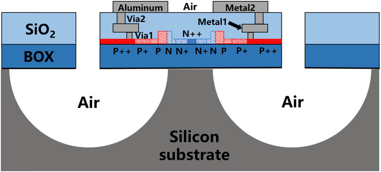
Fig. 2. Microwave electrical mode distribution of the TWMZM cross section (a) before and (b) after the silicon substrate is removed.

下载图片 查看原文

Fig. 3. Microwave attenuation based on finite element method (FEM) simulations on unloaded CPS transmission lines before and after substrate removing of the wafer used in our design.

下载图片 查看原文

Fig. 4. Simulated EO S21 before and after substrate removal of the wafer used in our design.

下载图片 查看原文

Fig. 5. Fabrication process of the substrate removed modulator based on IME’s silicon photonics platform.

下载图片 查看原文

Fig. 6. Micrograph of the fabricated substrate removed silicon modulator viewed from above and the enlarged picture of the (a) edge couple, (b) phase shifter, and (c) the electrode region.

下载图片 查看原文

Fig. 7. (a) Measured EE S21 of the substrate removed modulator under various bias voltages. (b) Microwave index of the modulator before and after the silicon substrate is removed, which is extracted from the tested EE S21 at 4  V bias voltage. (c) Electrode characteristic impedance of the modulator before and after the silicon substrate is removed, which is calculated from the tested EE S21 and S11 at 4  V bias voltage.

下载图片 查看原文

Fig. 8. Measured EO S21 response under various bias voltages after the silicon substrate is removed.

下载图片 查看原文

Fig. 9. Experimental setup for the substrate removed TWMZM OOK eye-diagram measurements.

下载图片 查看原文

Fig. 10. Optical eye diagrams at the different rates of 70  GBaud/s, 80  GBaud/s, and 90  GBaud/s under the driving voltage of 5 V Vpp without any pre-emphasis under bias voltage of 6  V. The extinction ratios are 3.6 dB, 2.7 dB, and 3.3 dB, respectively.

下载图片 查看原文

Fig. 11. Experimental setup for the substrate removed TWMZM PAM-4 eye-diagram measurements.

下载图片 查看原文

Fig. 12. Measured PAM-4 modulation optical eye diagrams at 28  GBaud/s, 50  GBaud/s, and 56  GBaud/s without any pre-emphasis under bias voltage of 6  V. The extinction ratios are 3.6 dB, 2.5 dB, and 2.7 dB, respectively.

下载图片 查看原文

Fig. 13. Experimental setup for the PAM-4 signal transmission based on the substrate removed silicon modulator even different distances.

下载图片 查看原文

Fig. 14. Measured curve of BER versus the received optical power for 56  GBaud/s (112  Gb/s) PAM-4 signal transmission under bias voltage of 6  V.

下载图片 查看原文

Fig. 15. Measured curve of BER versus the received optical power for 64  GBaud/s (128  Gb/s) PAM-4 signal transmission under bias voltage of 6  V.

下载图片 查看原文

Miaofeng Li, Lei Wang, Xiang Li, Xi Xiao, Shaohua Yu. Silicon intensity Mach–Zehnder modulator for single lane 100  Gb/s applications[J]. Photonics Research, 2018, 6(2): 02000109.

本文已被 3 篇论文引用
被引统计数据来源于中国光学期刊网
引用该论文: TXT   |   EndNote

相关论文

加载中...

关于本站 Cookie 的使用提示

中国光学期刊网使用基于 cookie 的技术来更好地为您提供各项服务,点击此处了解我们的隐私策略。 如您需继续使用本网站,请您授权我们使用本地 cookie 来保存部分信息。
全站搜索
您最值得信赖的光电行业旗舰网络服务平台!