Micro/nanostructure-based optical elements, such as meta-devices, are very useful for light field manipulation[1–8" target="_self" style="display: inline;">–8]. The feature size of the structures is required to be smaller than the wavelength of light. Fabrication of this kind of micro/nanostructures is still a challenge considering the balance of cost and yield[9–13" target="_self" style="display: inline;">–13]. Maskless optical lithography, using a focused laser spot to write arbitrary patterns on the organic photoresist thin films, is an effective method for the fabrication of micro/nanostructures on optical elements[14,15]. However, the resolution is generally limited to be at the wavelength scale due to the optical diffraction limit. Laser heat-mode lithography is an alternative way for obtaining subwavelength structures through thermally induced structural change, which is different from the photochemical exposure model in traditional optical lithography. The feature size of structures can be smaller than the laser spot due to the combination of the thermal threshold effect of laser heat-mode resist material and the Gaussian intensity profile of the laser spot itself[16–23" target="_self" style="display: inline;">–23].
The heat-mode resists are required to have good film-forming ability, excellent threshold characteristics of structural change, and etching selectivity between laser-irradiated and non-irradiated regions. Several Te-based chalcogenides heat-mode resists, such as AgInSbTe, GeSbTe, GeSbTeO, and GeSbTeBi[24–32" target="_self" style="display: inline;">–32], were proposed recently. However, due to the low melting temperature and high vapor pressure of the Te element, the Te-based multi-element alloys have some difficulties in smelting and machining of the sputtering target, controlling the composition segregation, and film forming. Besides, the pollution caused by the toxic Te element to the environment and semiconductor processing is still unavoidable[33]. Hence, exploring new Te-free heat-mode resist materials is of great importance for the application of laser heat-mode lithography. In this work, due to the simple element compositions and low crystallization temperature[34], a Te-free binary phase change material SbBi was proposed and investigated systematically as a new laser heat-mode resist.
SbBi thin films were deposited on glass substrates by a radio frequency magnetron sputtering method at room temperature at a background pressure of approximately . A sputtering power of 40 W and a working pressure of 0.5 Pa in the Ar environment were used during the sputtering process. The direct laser writing was conducted by a home-made laser writing system with the spot size of 1 μm on the SbBi films in air. A semiconductor GaN diode laser with a wavelength of 405 nm was used as the writing light source. Wet-etching (development) was conducted in 17% (mass fraction) solution. The etching depth was measured by a step profiler (D-100, KLA-Tencor). The morphology of the samples was observed by an atomic force microscope (AFM, Multimode V, Veeco) in the tapping mode. The absorption light spectrum from 300 to 800 nm was measured by a light spectrophotometer (Perkin-Elmer Lambda 1050UV/VIS/NIR). The crystal structures were studied by X-ray diffraction (XRD, D/MAX2500PC, Rigaku). The arbitrary patterns were observed by scanning electronic microscopy (SEM, JSM-6360LV, JEOL).
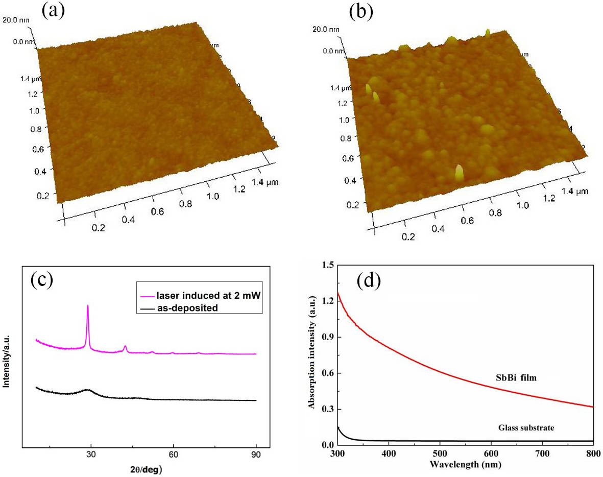
In laser heat-mode lithography, the resist materials are required to have good film-forming ability. Figures 1(a) and 1(b) give the AFM images of surface morphologies of as-deposited and laser-irradiated SbBi thin films with a 100 nm thickness, respectively. The as-deposited thin film presents a very smooth surface with a root-mean-squared (RMS) surface roughness of 0.9 nm, indicating that SbBi binary alloy materials have good film-forming ability. When the thin film is irradiated with a laser power of 2.0 mW at the continuous light mode, the SbBi thin film shows a surface with an RMS of 1.8 nm, and some small crystal grains appear, indicating that the film has been crystallized. It is further firmed by XRD analysis. As shown in Fig. 1(c), no diffraction peak can be observed for the as-deposited thin film (black curve). For comparison, the red curve displays the XRD spectrum of the sample irradiated by a laser beam. The obvious diffraction peaks reveal that SbBi is switched from an amorphous to crystalline state by the heat of the blue laser. The UV-visible absorption spectrum of as-deposited SbBi thin film is measured and compared with that of the glass substrate, as shown in Fig. 1(d). Compared with the negligible absorption of the glass substrate, the absorption of SbBi thin film is strong enough in the whole visible wavelength range, although it decreases with the increase of the light wavelength from 300 to 800 nm. This strong absorption indicates that the laser heat-mode lithography can be conducted at 405 nm light wavelength since the thin film can absorb laser energy effectively and convert the laser energy into heat, which can lead to structural changes.
Fig. 1. Basic characteristics of SbBi thin films. The AFM images of (a) as-deposited and (b) laser-irradiated SbBi thin films; (c) XRD patterns of as-deposited and laser-irradiated SbBi thin films; (d) absorption spectra of as-deposited SbBi thin film sample and glass substrate.
下载图片 查看所有图片
The wet-etching selectivity of SbBi thin films is crucial for laser heat-mode lithography. In order to investigate the wet-etching selectivity, the SbBi thin film was exposed by a laser spot at 2 mW. The wet-etching was conducted in 17% solution. Figure 2 presents the experimental results, where the etching depth changes with etching time. For laser-irradiated SbBi thin films, the etching rate is calculated to be 0.013 nm/s, and for as-deposited SbBi thin films, the etching rate is about 0.198 nm/s. The etching selectivity ratio of the as-deposited state to the laser-irradiated state is about 15:1, indicating that the amorphous state of SbBi film is more sensitive than the crystalline state. This result demonstrates that patterned structures can be effectively formed on exposed SbBi thin films by etching with solution. SbBi thin film is an excellent negative photoresist material.
Fig. 2. Comparison of wet-etching selectivity in 17% solution between as-deposited and laser-irradiated SbBi thin films. The laser irradiation power is fixed at 2 mW.
下载图片 查看所有图片
It is well known that is an alkaline solution in the wet-etching process, so both the amorphous state and crystalline state will be oxidized and then formed into acidic oxides, respectively[35]. Meanwhile, compared with the crystalline state, the long disordered structures in the amorphous state lead to more loose structures, which induces the etching reaction of the amorphous state to be easier than that of the crystalline state.
The dot and line patterns are written on the as-deposited SbBi thin films, and then the patterns are further etched for 5 min in 17% solution. Figure 3 presents the AFM images of the experimental results. Figure 3(a) shows an AFM image of a line array before wet-etching, where the writing laser power was 2 mW, and the writing speed was 1 mm/s. The linewidth is about 470 nm, which is smaller than that of the writing spot. One can see that the height in the laser-irradiated regions is slightly smaller than that in non-irradiated regions. The height difference is about 5 nm, as shown in the cross-sectional profile of Fig. 3(a). This is attributed to the fact that the laser irradiation causes crystallization, and the density of the crystalline state is larger than that of the as-deposited state. Figure 3(b) presents the AFM image of the film after wet-etching for 5 min in 17% solution. The un-irradiated (as-deposited) regions have been removed, while the laser-irradiated regions have been retained. The patterns present uniform and clear convex line-shaped structures. The cross-sectional analysis indicates that the linewidth can be as low as 310 nm, while the height is about 45 nm. The linewidth of 310 nm is a little smaller than that before wet-etching and is also smaller than the writing spot size due to the effect of the thermal threshold effect of laser heat-mode lithography.
Fig. 3. AFM images of fabricated structures on SbBi thin films: (a) line-type patterns without wet-etching; (b) line-type structures after wet-etching for 5 min in 17% solution; (c) dot-type structures after wet-etching for 5 min in 17% solution.
下载图片 查看所有图片
Uniform dot-shaped arrays have also been fabricated via the laser pulsed writing mode with a laser power of 2.5 mW and pulse width of 60 ns. Figure 3(c) displays the AFM image of the dot-shaped patterns after wet-etching for 5 min in 17% solution. The diameter and height of the dots are about 390 and 80 nm, respectively.
Compared to traditional laser direct writing, laser heat-mode lithography can overcome the optical diffraction limit, and both the linewidth and the period of gratings can be reduced by controlling the temperature field. The temperature field distribution of the laser-irradiated regions is presented in Fig. 4(a). To further study the effect of thermal diffusion between the adjacent two lines on the individual feature size in the process of writing, grating structures with a small period of 0.8 μm have been fabricated with a laser power of 1.8 mW and a writing speed of 0.8 mm/s. The grating lines after wet-etching are shown in Fig. 4(b). One can see that uniform periodical structures with the individual feature size of about 275 nm can be obtained, which confirms that thermal interference does not affect the adjacent microstructures obviously even when the laser spots overlap.
Fig. 4. (a) Principle of preparation of small-period grating structures; (b) AFM image of grating structures with a period of 0.8 μm.
下载图片 查看所有图片
The arbitrary patterns were fabricated successfully on the SbBi thin films by the pulsed writing mode, as shown in Fig. 5. Figures 5(a) and 5(b) are original pictures of the Star of David and the logo of the Chinese Academy of Sciences (CAS), respectively. Figures 5(c) and 5(d) are the SEM images of the fabricated structures. The laser power is fixed at 2.5 mW, and the laser pulse width is 60 ns. One can see that the fabricated structures are very clear and similar to their original pictures.
Fig. 5. Images of complex pattern structures. The original pictures of (a) the Star of David and (b) logo of CAS. The structures fabricated on SbBi thin films: (c) the Star of David and (d) logo of CAS.
下载图片 查看所有图片
In conclusion, Te-free SbBi thin films were used as laser heat-mode lithography resist. For SbBi binary alloy thin films, the thermally induced structural change from an amorphous to crystalline state happens through laser irradiation induced heating. The etching selectivity ratio of the as-deposited state to the laser-irradiated state in 17% solution is about 15:1. Based on the etching selectivity, the line-type, dot-type, and complex patterns are fabricated on SbBi thin films by laser heat-mode lithography. Grating structures with a linewidth of 275 nm and a period of 0.8 μm demonstrated that thermal diffusion between the adjacent two lines has almost no effect on the individual feature size in the process of writing. These results indicate that SbBi thin films are excellent laser heat-mode lithography materials for fabrication of micro/nanostructures.
Kui Zhang, Zhengwei Wang, Guodong Chen, Yang Wang, Aijun Zeng, Jing Zhu, Syarhei Avakaw, Heorgi Tsikhanchuk. Te-free SbBi thin film as a laser heat-mode photoresist[J]. Chinese Optics Letters, 2019, 17(9): 093102.
 Download: 856次


