红外与毫米波学报, 2024, 43 (1): 85, 网络出版: 2023-12-26  

一种改进的基于110 GHz在片S参数测试的HEMT器件寄生电阻提取方法

An improved method for determination of extrinsic resistances for HEMT devices based on 110 GHz S-parameters on-wafer measurement
作者单位
1 华东师范大学 物理与电子科学学院,上海 200241
2 南通大学 交通与土木工程学院,江苏 南通 226019
摘要
提出了一种改进的高电子迁移率晶体管寄生电阻提取方法,该方法利用了特殊偏置点(Vgs > Vth,Vds = 0 V)的等效电路模型,推导了寄生电阻的表达式,采用半分析法对寄生电阻进行了优化。1 ~110 GHz S参数实测结果和仿真的S参数一致,证明该方法是有效的。
Abstract
An improved method for determination of extrinsic resistances for 70 nm InP high electron mobility transistor (HEMT) is proposed in this paper. A set of expressions have been derived from the equivalent circuit model under operating bias points (Vgs > Vth, Vds = 0 V). The extrinsic resistances are iterative determined using the discrepancy between simulated and measured S-parameters as an optimization criterion using the semi-analytical method. Good agreement between simulated and measured S-parameters under multi bias over the frequency range up to 110 GHz verifies the effectiveness of this extraction method.

1 Introduction

Accurate extrinsic resistances extraction for modeling InP HEMT devices is a crucial step in the design and production of high-yield,low-cost millimeter wave circuits1. The common used methods mainly include numerical optimization method,cold FET method and cutoff method. In optimization method,the extrinsic resistances extraction result strongly depends on the initial value and suffers from non-uniqueness and non-physical meaning2. In cold FET method,the large gate currents caused by forward-biased run through the gate Schottky junction,which leads to degradation of the gate3-6. To avoid degradation of device characteristics,some authors proposed cutoff method to extract extrinsic resistances. However,this method is valid only at high frequency(>18GHz),and the extracted resistances fluctuate widely over the whole frequency range of interest7-9.

In order to overcome these limitations,an improved method for determination of extrinsic resistances is proposed. In contrast with previous publications,this extraction method offers the following advantages.

1)Under operating bias point(Vgs > Vth,Vds = 0 V),the effect of channel between source and drain can be modeled by resistance Rch,while the capacitance will be dominant under cutoff bias condition.

2)The semi-analytical method which is a combination of optimization method and analytical direct extraction method has been used to determine the extrinsic resistances.

3)This extraction method is verified with S-parameters on-wafer measurement up to 110 GHz.

Section Ⅱ gives the equivalent circuit model under operating bias point(Vgs > Vth,Vds = 0 V)as well as the derivation of analytical expressions. Section Ⅲ gives the procedure of intrinsic parameters extraction. The measured and simulated results are presented in Section Ⅳ. The conclusion is given in Section Ⅴ.

1 Extrinsic resistances extraction

1.1 Equivalent circuit model
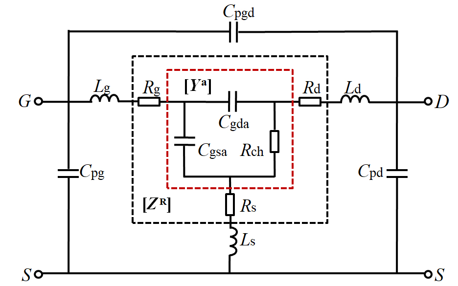
Fig.1 shows the small-signal equivalent circuit model under operating bias point(Vgs > Vth,Vds = 0 V). CpgdCpg,and Cpd represent the extrinsic capacitances due to the pad connections. LgLd,and Ls represent the extrinsic inductances of the gate,drain,and source feedlines. Rs and Rd represent the extrinsic resistances of the source and drain. Rg is the distributed gate resistance. Cgsa and Cgda represent intrinsic gain-source and gain-drain capacitances respectively. Rch is the channel resistance when the channel between drain and source is open at zero drain bias and gate voltage above threshold voltage.

图 1. 偏置点(Vgs > Vth,Vds = 0 V)下的小信号等效电路模型

Fig. 1. The small-signal equivalent circuit model under operating bias point(Vgs > Vth,Vds = 0 V)

下载图片 查看所有图片

The intrinsic part of the equivalent circuit model,which exhibits a PI topology,so it is convenient to describe it by a Y matrix as:

,

Convert -parameters to -parameters:

,,,,

The Z-parameters of intrinsic part with extrinsic resistances can be expressed as following:

,,,,

Therefore,we have

,,,

By neglecting the high order term ,the extrinsic resistances can be obtained by analytical expressions from real part of -parameters:

,,,

where

,,

Cgsa and Cgda can be determined at low frequencies:

,,

1.2 Extrinsic parameters extraction

The pad capacitances can be determined by measuring an open test structure:

,,,

The extrinsic inductances LgLd,and Ls can be determined from the imaginary part of Z-parameters(transformed from measured S-parameters)of the short test structure directly:

,,,

The extraction of extrinsic resistances can be based on the semi-analytical method which is a combination of optimization method and analytical direct extraction method. The extraction procedure is as follows.

1)De-embedding the pad capacitances and feedline inductances.

2)Set the initial value of the channel resistance Rch .

3)Calculate the extrinsic resistances RgRd,and Rs using(13)-(15)which can be expressed as functions of Rch as well as frequency.

4)Set error criteria as follows:

,

Where represents the calculated S-parameters,and represents the measured S-parameters. represents the discrepancy between simulated and measured S-parameters. Wpq are the weighting factors.

5)If error criteria are small enough,the iterative process will be end.

图 2. 算法流程图

Fig. 2. Flow chart of the algorithm

下载图片 查看所有图片

2 Intrinsic parameters extraction

The small-signal circuit model of intrinsic part of InP HEMT devices is illustrated in Fig. 3 after de-embedding the extrinsic parameters,and the intrinsic Y-parameters are described as3

,,,,

图 3. 本征部分的小信号等效电路模型

Fig. 3. The small-signal circuit model of intrinsic part

下载图片 查看所有图片

with

From the analytical expressions(27)-(30),the intrinsic element values can be obtained directly.

3 Results and discussion

In this paper,70 nm InP HEMT devices have been used with 2×30 μm gate width(number of gate fingers×unit gate width). The S-paremeters on-wafer measurement up to 110 GHz using N5247 network analyzer with DC bias by an Agilent B1500A.

Fig. 4 shows the plot of extracted extrinsic resistances versus frequency using the presented semi-analytical method and cutoff method9. As can be seen from Fig. 4,the extracted Rd and Rs using semi-analytical method are nearly constant versus frequency,while extracted Rd and Rs using cutoff method fluctuate widely versus frequency. These results verify that the proposed extraction method is better than cutoff method 10.

图 4. 半分析方法和截止方法提取的寄生电阻数值对比

Fig. 4. Extracted extrinsic resistances using the proposed semi-analytical method and cutoff method

下载图片 查看所有图片

Table 1 gives the values of extrinsic resistances extracted using semi-analytical method. The values of extrinsic capacitances and inductances are given in Table 2. The extracted intrinsic parameters in Section III are shown in Table 3.

表 1. 寄生电阻数值

Table 1. The values of extrinsic resistances

ElementValue
2.66
4.18
3.80

查看所有表

表 2. 寄生电容和寄生电感数值

Table 2. The values of extrinsic capacitance and inductance

CapacitanceValuesInductanceValues
13.2622.7
13.1928.5
0.4163.25

查看所有表

表 3. 本征元件数值

Table 3. The values of intrinsic parameters

ElementValueElementValue
46.9782.2
9.695.20
15.783.46

查看所有表

表 4. S参数精度

Table 4. Accuracy of S-parameters

Bias ConditionS11S12S21S22
5.45%1.55%4.37%2.59%
5.46%1.46%4.26%2.45%
4.99%1.85%4.80%2.74%
5.82%1.97%4.97%4.04%

查看所有表

The intrinsic elements listed in Table 2 are substituted into the equivalent circuit model for simulation. Fig. 5 shows the comparison between simulated and measured S-parameters under multi bias. Good agreement between simulated and measured S-parameters are observed in the frequency range of 1 GHz to 110 GHz,which verifies the validity of this developed method to determine the extrinsic resistances.

图 5. 1 GHz ~110 GHz 频率范围内多偏置下模拟和测量S参数对比曲线

Fig. 5. Comparison between simulated (lines) and measured (squares) S-parameters over the frequency range going:from 1 GHz to 110 GHz under multi bias

下载图片 查看所有图片

Table 4 outlines a selection of the accuracy of S-parameters for four different bias points. As can been seen from this table,S11 and S21 maintain an accuracy of around 5%,S12 has an accuracy of less than 5%,and S22 has an accuracy of between 2%~5%.

4 Conclusion

An approach for determination of extrinsic resistances for 70 nm InP HEMT devices is proposed in this paper. Extrinsic resistances are described as functions of the intrinsic channel resistance,and optimum values can be obtained using semi-analytical method under operating bias point(Vgs > Vth,Vds = 0 V). Verification of this extraction method is presented by the good agreement between the simulated and measured S-parameters under multi bias over the frequency range up to 110 GHz.

参考文献

[1] Debie P, Martens L. Fast and accurate extraction of parasitic resistances for nonlinear GaAs-MESFET device models[J]. IEEE Transactions on Electron Devices, 1995, 42(12): 2239-2242.

[2] Niekerk C V, Meyer P. Performance and limitations of decomposition based parameter-extraction procedures for FET small-signal models[J]. IEEE Transactions on Microwave Theory and Techniques, 1998, 46(11): 1620-1627.

[3] Dambrine, G, Cappy, et al. A new method for determining the FET small-signal equivalent circuit[J]. IEEE Transactions on Microwave Theory and Techniques, 1988.

[4] Anholt R, Swirhun S. Equivalent-circuit parameter extraction for cold GaAs MESFET's[J]. IEEE Transactions on Microwave Theory and Techniques, 1991, 39(7): 1243-1247.

[5] Yanagawa S, Ishihara H, Ohtomo M. Analytical method for determining equivalent circuit parameters of GaAs FETs[J]. IEEE Transactions on Microwave Theory & Techniques, 1996, 44(10): 1637-1641.

[6] Jeon M Y, Kim B G, Jeon Y J. A Technique for Extracting Small-Signal Equivalent-Circuit Elements of HEMTs[J]. IEICE Transactions on Electronics, 1999, 82(11): 1968-1976.

[7] Tayrani, GerberReza, DanielJason E., PengellyTom, RohdeRayrnond S., UlrichL. A new and reliable direct parasitic extraction method for MESFETs and HEMTs [C]. European Microwave Conference. IEEE, 1993. 10.1109/euma.1993.336593

[8] Kim C H, Yoon K S. A new extraction method to determine bias-dependent source series resistance in GaAs FET's[J]. IEEE Transactions on Microwave Theory & Techniques, 1998, 46(9): 1242-1250.

[9] Gao J, Law C L, Wang H, et al. An Improved Pinchoff Equivalent Circuit Model for Determining PHEMT Model Parameters for Millimeterwave Application[J]. International Journal of Infrared & Millimeter Waves, 2002, 23(11): 1611-1626.

[10] GaoJ. RF and Microwave Modeling and Measurement Techniques for Field Effect Transistors [M]. IET Digital Library, 2010. 10.1049/sbew027e

李织纯, 吕渊婷, 张傲, 高建军. 一种改进的基于110 GHz在片S参数测试的HEMT器件寄生电阻提取方法[J]. 红外与毫米波学报, 2024, 43(1): 85. Zhi-Chun LI, Yuan-Ting LYU, Ao ZHANG, Jian-Jun GAO. An improved method for determination of extrinsic resistances for HEMT devices based on 110 GHz S-parameters on-wafer measurement[J]. Journal of Infrared and Millimeter Waves, 2024, 43(1): 85.

引用该论文: TXT   |   EndNote

相关论文

加载中...

关于本站 Cookie 的使用提示

中国光学期刊网使用基于 cookie 的技术来更好地为您提供各项服务,点击此处了解我们的隐私策略。 如您需继续使用本网站,请您授权我们使用本地 cookie 来保存部分信息。
全站搜索
您最值得信赖的光电行业旗舰网络服务平台!