激光与光电子学进展, 2020, 57 (11): 111430, 网络出版: 2020-06-02
飞秒激光过饱和掺杂硅基光电探测器研究进展  下载: 1581次特邀综述
Research Progress on Hyperdoped Silicon Photodetectors Fabricated by Femtosecond Laser
图 & 表
图 1. 脉冲激光熔化和再固化过程中掺杂剂扩散过程的示意图[24]
Fig. 1. Schematic of dopant diffusion process during pulsed-laser melting and resolidification[24]
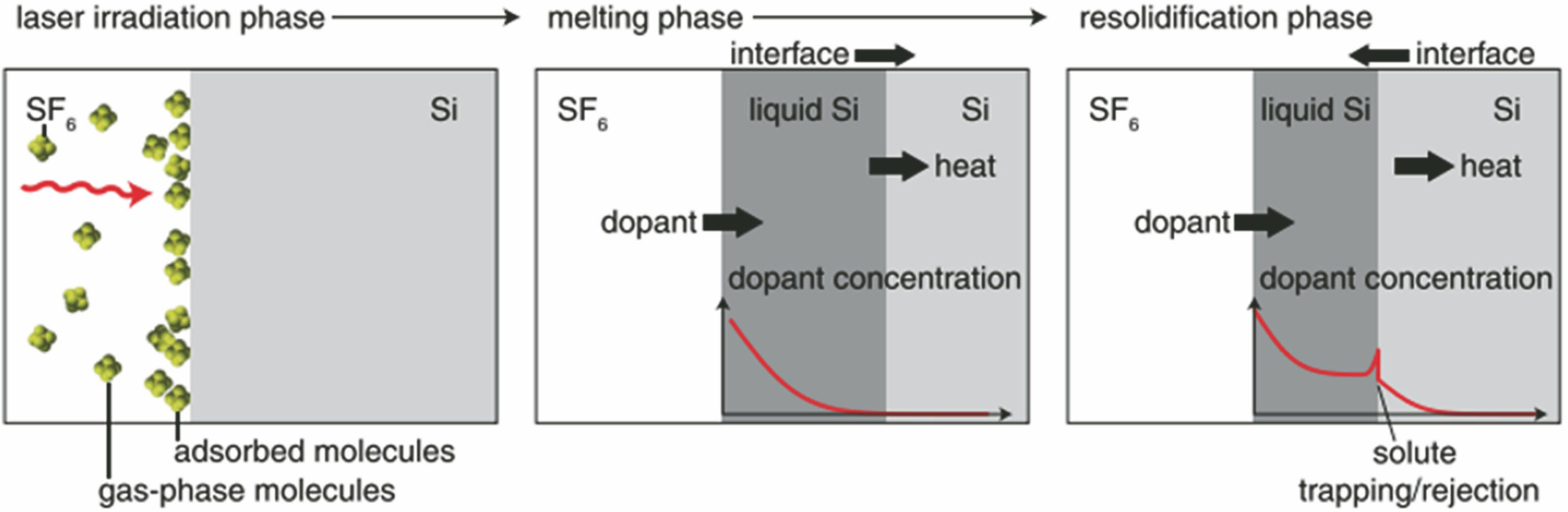
图 2. 黑硅表面的选区电子衍射图像和结电流电压特性[20]。(a)退火前和(b) 退火后(975 K,30 min)黑硅表面的选区电子衍射图像;(c)激光掺杂区与p型衬底之间的结电流电压特性
Fig. 2. Selected area electron diffraction images of black silicon surface and current-voltage properties of junction[20]. Selected area electron diffraction images of black silicon surface (a) before and (b) after annealing (975 K,30 min); (c) current-voltage properties of junction between laser-doped region and p-type substrate

图 3. 黑硅光电探测器的光电性质。(a)无掺杂黑硅光电探测器的明暗电流随电压变化的特性[37];(b)过饱和掺银硅基光电探测器的亚带隙光谱响应度与光子能量的关系,且观察到一个阈值能量为0.82 eV的扭结[38]
Fig. 3. Photoelectric properties of black silicon photodetectors. (a) Photocurrent and dark current versus voltage for non-doped black silicon photodetector[37]; (b) sub-band gap spectral responsivity as a function of photon energy for Ag-hyperdoped silicon-based photodetector. A kink with the threshold energy of 0.82 eV is obtained[38]

图 4. 飞秒激光过饱和掺硫的硅基光电探测器器件性能[39]。(a)不同偏压下黑硅光电探测器的响应度以及与商用硅、锗探测器的对比;插图分别为黑硅光电探测器的峰值响应(左)和红外响应(右)随偏压的变化趋势;(b)黑硅光电探测器的光电流和暗电流随偏压的变化趋势
Fig. 4. Device performance of sulfur-hyperdoped silicon-based photodetector prepared by femtosecond laser[39]. (a) Responsivities for a black silicon photodetector under different bias voltages and comparison with commercial silicon and germanium photodetectors. The insets show the peak responsivity (left) and infrared responsivity (right) versus bias voltage; (b) photocurrent and dark current versus bias voltage for the black silicon photodetector

图 5. 纳秒激光退火对晶格结构的影响[48]。(a)高结晶度的过饱和掺杂硅的晶格结构;(b)宽谱段吸收光谱
Fig. 5. Effect of nanosecond laser annealing on lattice structure[48]. (a) Lattice structure of hyperdoped silicon with high crystallinity; (b) corresponding broad-spectral light absorptance

图 6. 硫氮共掺的黑硅材料。(a)硫氮共掺的过饱和掺杂硅的晶格结构[52];基于共掺黑硅制备的光电探测器的(b)示意图和(c)光响应度曲线[54]
Fig. 6. Sulfur-nitrogen co-doped black silicon material. (a) Lattice structure of hyperdoped silicon co-doped with sulfur and nitrogen[52]; (b) diagram and (c) photoresponsivity curve of photodetector based on co-doped black silicon[54]

图 7. 高温条件下制备的掺Te黑硅材料及其光电探测器[55]。(a)在700 K下飞秒激光过饱和掺杂的单晶黑硅的晶格结构;(b)单晶黑硅探测器与商用探测器的响应度对比
Fig. 7. Te-doped black silicon material and photodetector prepared at high temperature. (a) Lattice structure of single crystal black silicon hyperdoped with femtosecond laser at 700 K [55]; (b) comparison of responsivity of commercial detectors with single crystal black silicon detector

图 8. 柔性单晶硅与柔性黑硅。(a)超薄柔性单晶硅易弯曲、可裁剪的弯曲性能展示[62];(b)飞秒激光辐照SOI硅片制备的柔性黑硅在化学腐蚀前后光吸收率[67]
Fig. 8. Flexible single crystal silicon and flexible black silicon. (a) Bending performance of flexible and tailorable ultra-thin single crystal silicon[62]; (b) light absorption of flexible black silicon fabricated by femtosecond laser irradiating SOI wafer before and after chemical etching[67]

图 9. 高性能的过饱和掺硫柔性硅基光电探测器[68]。(a)柔性黑硅光电探测器示意图及材料的表面形貌;(b)不同弯曲半径下柔性黑硅探测器在多个波长的光响应
Fig. 9. High-performance sulfur-hyperdoped flexible silicon-based photodetector[68]. (a) Diagram of flexible black silicon photodetector and surface morphology of the material; (b) photoresponsivity of flexible black silicon photodetector at various wavelengths for different bending radii

进晓荣, 吴强, 黄松, 贾子熙, 宋冠廷, 周旭, 姚江宏, 许京军. 飞秒激光过饱和掺杂硅基光电探测器研究进展[J]. 激光与光电子学进展, 2020, 57(11): 111430. Xiaorong Jin, Qiang Wu, Song Huang, Zixi Jia, Guanting Song, Xu Zhou, Jianghong Yao, Jingjun Xu. Research Progress on Hyperdoped Silicon Photodetectors Fabricated by Femtosecond Laser[J]. Laser & Optoelectronics Progress, 2020, 57(11): 111430.


 PDF全文
PDF全文

