Photonics Research, 2019, 7 (11): 11000B73, Published Online: Oct. 28, 2019
Scanning electron microscopy as a flexible technique for investigating the properties of UV-emitting nitride semiconductor thin films  Download: 807次
Figures & Tables
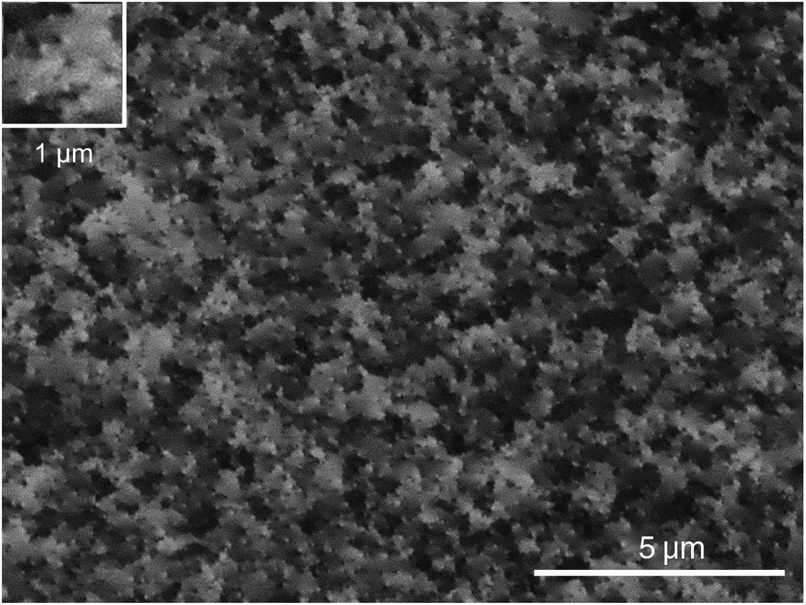
Fig. 2. (a) SE image of nPSS, (b) schematic of overgrowth of AlN on nPSS, and (c) ECCI micrograph from an AlN thin film. Inset is on the same scale but with higher resolution.

Fig. 3. EBSD maps from the AlN/nPSS thin film: (a) grain reference orientation deviation (GROD) map and (b) GROD axis map relative to the sample normal (c -axis, [0001] direction]) where the colors denote direction of in-plane rotation (i.e., around the c -axis). The red regions are rotated in the opposite direction to the blue regions as indicated.

Fig. 4. (a) Schematic of semi-polar GaN microrod template and overgrowth, indicating the distribution of stacking faults on the surface of the sample and the crystallographic directions. (b) ECCI micrograph revealing stacking faults. (c) Example CL spectra from a dark stripe and a bright stripe, respectively. The boxes on (d) indicate where the spectra were extracted from the CL dataset. (d) Integrated CL intensity image of the GaN near band edge (NBE) emission (3.15–3.50 eV) on the same scale as (e) but not from the same area. (e) Higher resolution ECCI micrograph revealing dislocations. (f) Integrated CL intensity image of the GaN near band edge (NBE) emission (3.15–3.50 eV) on the same scale as (e) but not from the same area.

Fig. 5. (a) Schematic of the sample structure. x = 0.82

Fig. 6. WDX maps of the intensities of (a) Ga L α K α c -plane AlGaN sample, with an average AlN content of 81%. The scale bar for X-ray intensities applies to both WDX maps, although with different absolute values.

Fig. 7. (a) Semi-log plot showing the measured Si content in the GaN layers, calibrated using the points where SIMS data is available (red data points). (b) Long qualitative scan for Si for the sample with lowest measured Si content 2.3 × 10 17 cm − 3

C. Trager-Cowan, A. Alasmari, W. Avis, J. Bruckbauer, P. R. Edwards, B. Hourahine, S. Kraeusel, G. Kusch, R. Johnston, G. Naresh-Kumar, R. W. Martin, M. Nouf-Allehiani, E. Pascal, L. Spasevski, D. Thomson, S. Vespucci, P. J. Parbrook, M. D. Smith, J. Enslin, F. Mehnke, M. Kneissl, C. Kuhn, T. Wernicke, S. Hagedorn, A. Knauer, V. Kueller, S. Walde, M. Weyers, P.-M. Coulon, P. A. Shields, Y. Zhang, L. Jiu, Y. Gong, R. M. Smith, T. Wang, A. Winkelmann. Scanning electron microscopy as a flexible technique for investigating the properties of UV-emitting nitride semiconductor thin films[J]. Photonics Research, 2019, 7(11): 11000B73.


 PDF全文
PDF全文

