
Author Affiliations
Abstract
1 School of Information Science and Technology, ShanghaiTech University, Shanghai 201210, China
2 Shanghai Institute of Microsystem and Information Technology, Chinese Academy of Sciences, Shanghai 200050, China
3 School of Microelectronics, University of Chinese Academy of Sciences, Beijing 100049, China
4 School of Electronics and Information Technology, Sun Yat-sen University, Guangzhou 510275, China
Emission and capture characteristics of a deep hole trap (H1) in n-GaN Schottky barrier diodes (SBDs) have been investigated by optical deep level transient spectroscopy (ODLTS). Activation energy (Eemi) and capture cross-section (σp) of H1 are determined to be 0.75 eV and 4.67 × 10?15 cm2, respectively. Distribution of apparent trap concentration in space charge region is demonstrated. Temperature-enhanced emission process is revealed by decrease of emission time constant. Electric-field-boosted trap emission kinetics are analyzed by the Poole?Frenkel emission (PFE) model. In addition, H1 shows point defect capture properties and temperature-enhanced capture kinetics. Taking both hole capture and emission processes into account during laser beam incidence, H1 features a trap concentration of 2.67 × 1015 cm?3. The method and obtained results may facilitate understanding of minority carrier trap properties in wide bandgap semiconductor material and can be applied for device reliability assessment.
GaN deep level transient spectroscopy minority carrier trap time constant trap concentration Journal of Semiconductors
2024, 45(3): 032503
Author Affiliations
Abstract
1 Institute of Microelectronics, Chinese Academy of Sciences, Beijing 100029, China
2 University of Chinese Academy of Sciences, Beijing 100049, China
In this work, a novel one-time-programmable memory unit based on a Schottky-type p-GaN diode is proposed. During the programming process, the junction switches from a high-resistance state to a low-resistance state through Schottky junction breakdown, and the state is permanently preserved. The memory unit features a current ratio of more than 103, a read voltage window of 6 V, a programming time of less than 10?4 s, a stability of more than 108 read cycles, and a lifetime of far more than 10 years. Besides, the fabrication of the device is fully compatible with commercial Si-based GaN process platforms, which is of great significance for the realization of low-cost read-only memory in all-GaN integration.
wide-bandgap semiconductor one-time programmable Schottky-type p-GaN diode read-only memory device Journal of Semiconductors
2024, 45(3): 032502

Author Affiliations
Abstract
1 Department of Engineering “Enzo Ferrari”, University of Modena and Reggio Emilia, Modena 41125, Italy
2 Department of Information Engineering, University of Padova, Padova 35131, Italy
3 Department of Sciences and Methods for Engineering (DISMI), University of Modena and Reggio Emilia, Reggio Emilia 42122, Italy
4 EN & TECH Center, University of Modena and Reggio Emilia, Reggio Emilia 42122, Italy
5 Advanced Technologies and Micro Systems Department, Robert Bosch GmbH, Renningen 71272, Germany
Vertical GaN power MOSFET is a novel technology that offers great potential for power switching applications. Being still in an early development phase, vertical GaN devices are yet to be fully optimized and require careful studies to foster their development. In this work, we report on the physical insights into device performance improvements obtained during the development of vertical GaN-on-Si trench MOSFETs (TMOS’s) provided by TCAD simulations, enhancing the dependability of the adopted process optimization approaches. Specifically, two different TMOS devices are compared in terms of transfer-curve hysteresis (H) and subthreshold slope (SS), showing a ≈ 75% H reduction along with a ≈ 30% SS decrease. Simulations allow attributing the achieved improvements to a decrease in the border and interface traps, respectively. A sensitivity analysis is also carried out, allowing to quantify the additional trap density reduction required to minimize both figures of merit.
vertical GaN trench MOSFET SiO2 interface traps border traps hysteresis BTI Journal of Semiconductors
2024, 45(3): 032501
Author Affiliations
Abstract
1 Key Laboratory of Nanodevices and Applications, Suzhou Institute of Nano-tech and Nano-Bionics, Chinese Academy of Sciences, Suzhou 215123, China
2 School of Physical Science and Technology, ShanghaiTech University, Shanghai 201210, China
3 Shanghai Advanced Research Institute, Chinese Academy of Sciences, Shanghai 201210, China
4 University of Chinese Academy of Sciences, Beijing 100049, China
A new kind of step-flow growth mode is proposed, which adopts sidewall as step source on patterned GaN substrate. The terrace width of steps originated from the sidewall was found to change with the growth temperature and ammonia flux. The growth mechanism is explained and simulated based on step motion model. This work helps better understand the behaviors of step advancement and puts forward a method of precisely modulating atomic steps.
step-flow growth GaN terrace width step motion Journal of Semiconductors
2024, 45(2): 022501
Author Affiliations
Abstract
1 School of Nano-Tech and Nano-Bionics, University of Science and Technology of China, Hefei 230026, China
2 Suzhou Institute of Nano-Tech and Nano-Bionics, Chinese Academy of Sciences, Suzhou 215123, China
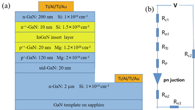
The InGaN films and GaN/InGaN/GaN tunnel junctions (TJs) were grown on GaN templates with plasma-assisted molecular beam epitaxy. As the In content increases, the quality of InGaN films grown on GaN templates decreases and the surface roughness of the samples increases. V-pits and trench defects were not found in the AFM images. p++-GaN/InGaN/n++-GaN TJs were investigated for various In content, InGaN thicknesses and doping concentration in the InGaN insert layer. The InGaN insert layer can promote good interband tunneling in GaN/InGaN/GaN TJ and significantly reduce operating voltage when doping is sufficiently high. The current density increases with increasing In content for the 3 nm InGaN insert layer, which is achieved by reducing the depletion zone width and the height of the potential barrier. At a forward current density of 500 A/cm2, the measured voltage was 4.31 V and the differential resistance was measured to be 3.75 × 10?3 Ω·cm2 for the device with a 3 nm p++-In0.35Ga0.65N insert layer. When the thickness of the In0.35Ga0.65N layer is closer to the “balanced” thickness, the TJ current density is higher. If the thickness is too high or too low, the width of the depletion zone will increase and the current density will decrease. The undoped InGaN layer has a better performance than n-type doping in the TJ. Polarization-engineered tunnel junctions can enhance the functionality and performance of electronic and optoelectronic devices.
GaN/InGaN/GaN tunnel junctions polarization-engineering molecular beam epitaxy Journal of Semiconductors
2024, 45(1): 012503

Author Affiliations
Abstract
National Key Laboratory of Solid-State Microwave Devices and Circuits, Hebei Semiconductor Research Institute, Shijiazhuang 050051, China
In this letter, high power density AlGaN/GaN high electron-mobility transistors (HEMTs) on a freestanding GaN substrate are reported. An asymmetric Γ-shaped 500-nm gate with a field plate of 650 nm is introduced to improve microwave power performance. The breakdown voltage (BV) is increased to more than 200 V for the fabricated device with gate-to-source and gate-to-drain distances of 1.08 and 2.92 μm. A record continuous-wave power density of 11.2 W/mm@10 GHz is realized with a drain bias of 70 V. The maximum oscillation frequency (fmax) and unity current gain cut-off frequency (ft) of the AlGaN/GaN HEMTs exceed 30 and 20 GHz, respectively. The results demonstrate the potential of AlGaN/GaN HEMTs on free-standing GaN substrates for microwave power applications.
freestanding GaN substrates AlGaN/GaN HEMTs continuous-wave power density breakdown voltage Γ-shaped gate Journal of Semiconductors
2024, 45(1): 012501

Author Affiliations
Abstract
1 State Key Laboratory of Mobile Network and Mobile Multimedia Technology, Shenzhen 518055, China
2 Wireless Product Planning Department, ZTE Corporation, Shenzhen 518055, China
3 School of Microelectronics, Xidian University, Xi’an 710071, China
The GaN HEMT is a potential candidate for RF applications due to the high frequency and large power handling capability. To ensure the quality of the communication signal, linearity is a key parameter during the system design. However, the GaN HEMT usually suffers from the nonlinearity problems induced by the nonlinear parasitic capacitance, transconductance, channel transconductance etc. Among them, the transconductance reduction is the main contributor for the nonlinearity and is mostly attributed to the scattering effect, the increasing resistance of access region, the self-heating effect and the trapping effects. Based on the mechanisms, device-level improvement methods of transconductance including the trapping suppression, the nanowire channel, the graded channel, the double channel, the transconductance compensation and the new material structures have been proposed recently. The features of each method are reviewed and compared to provide an overview perspective on the linearity of the GaN HEMT at the device level.
GaN HEMT linearity improvement transconductance reduction transconductance compensation nanowire channel graded channel Journal of Semiconductors
2023, 44(12): 121801
光子学报
2023, 52(12): 1210004
1 西南交通大学 信息科学与技术学院,四川 成都 611756
2 西南交通大学 数学学院,四川 成都 611756
由于射频信号种类多,电磁环境复杂,特征提取难度大,现有的基于人工特征的射频辐射源个体识别方法的鲁棒性、适用性难以满足应用需求。数据驱动的深度学习方法虽然可以提供更灵活的辐射源个体识别模式,但深度学习方法自身可解释性差,而且缺乏通用测试模式来评价一个深度学习方法的优劣。本文在电磁大数据非凡挑战赛目标个体数据集的基础上,探索了基于该数据集的深度学习模型测试方法,提出面向辐射源个体识别神经网络模型的通用测试系统架构。该构架通过信号特征遮掩、生成对抗网络(GAN)、欺骗信号汇集、信道模拟等方法构造仿真测试样本,并把测试样本与原样本数据导入深度模型进行识别结果对比测试。基于测试结果分析了深度模型聚焦的信号关键特征位置,分析模型的鲁棒性,揭示信道环境对识别性能的影响,从而解释了深度学习网络模型的性能。
辐射源个体识别 可解释性 生成对抗网络 无线信号欺骗 specific emitter identification interpretability Generative Adversarial Network(GAN) wireless signal spoofing 太赫兹科学与电子信息学报
2023, 21(6): 734


