Author Affiliations
Abstract
1 Institute of Microelectronics, Chinese Academy of Sciences, Beijing 100029, China
2 University of Chinese Academy of Sciences, Beijing 100049, China
In this work, a novel one-time-programmable memory unit based on a Schottky-type p-GaN diode is proposed. During the programming process, the junction switches from a high-resistance state to a low-resistance state through Schottky junction breakdown, and the state is permanently preserved. The memory unit features a current ratio of more than 103, a read voltage window of 6 V, a programming time of less than 10?4 s, a stability of more than 108 read cycles, and a lifetime of far more than 10 years. Besides, the fabrication of the device is fully compatible with commercial Si-based GaN process platforms, which is of great significance for the realization of low-cost read-only memory in all-GaN integration.
wide-bandgap semiconductor one-time programmable Schottky-type p-GaN diode read-only memory device Journal of Semiconductors
2024, 45(3): 032502
1 中国电子科技集团公司第十三研究所, 河北石家庄 050051
2 固态微波器件与电路全国重点实验室, 河北石家庄 050051
介绍了一款基于 GaAs肖特基二极管单片工艺的 220 GHz倍频器的设计过程以及测试结果。为提高输出功率, 倍频器采用多阳极结构, 8个二极管在波导呈镜像对称排列, 形成平衡式倍频器结构。采用差异式结电容设计解决了多阳极结构端口散射参数不一致问题, 提高了倍频器的转换效率和工作带宽。对设计的倍频器进行流片、装配和测试, 测试结果显示: 倍频器在 204~ 234 GHz频率范围内, 转化效率大于 15%; 226 GHz峰值频率下实现最大输出功率为 90.5 mW, 转换效率为 22.6%。设计的 220 GHz倍频器输出功率高, 转化效率高, 工作带宽大。
倍频器 太赫兹 肖特基二极管 结电容 单片 frequency doubler tearhertz Schottky barrier diode junction capacitance Microwave Monolithic Integrated Circuit 太赫兹科学与电子信息学报
2023, 21(9): 1080
1 北京智芯微电子科技有限公司, 北京 100080
2 国网重庆市电力公司营销服务中心,重庆 401121
3 西安交通大学, 西安 710049
提出了一种采用肖特基漏极(SD)与场板相结合、实现硅基垂直MOSFET器件反向阻断应用的技术。基于该技术,采用二维仿真提出并研究了两种新型垂直MOSFET器件,即带有垂直场板(VFP)的SD-VFP-MOS器件和带有倾斜场板(SFP)的SD-SFP-MOS器件。相比采用肖特基漏极的MOSFET (SD-MOS)和采用超结和肖特基漏极的MOSFET(SD-SJ-MOS),所提出的SD-VFP -MOS,尤其是SD-SFP-MOS,反向击穿电压有显著提高,且几乎不影响导通特性。开展了器件的开态电流密度、关态电势分布、关态电流密度和电场分布分析,揭示了VFP和SFP提高器件反向阻断能力的内在机理。详细讨论了场板结构参数对器件反向击穿电压和场板效率的影响,研究结果对于SD-VFP-MOS和SD-SFP-MOS的设计具有重要意义。
垂直MOSFET 肖特基漏极 场板 反向阻断 vertical MOSFET Schottky-drain field-plate reverse blocking
1 南京邮电大学理学院, 南京 210023
2 南京邮电大学材料科学与工程学院, 南京 210023
3 河南大学物理与电子学院, 开封 475004
利用基于密度泛函理论的第一性原理计算研究了不同层数MoS2和VS2堆垛形成的范德瓦耳斯异质结的电子结构和光学性能。通过从头算分子动力学验证了两种异质结在室温下的稳定性。此外, 两种异质结均显示p型肖特基接触, 但相较于单层MoS2构成的异质结, 在双层MoS2和VS2堆垛形成的异质结中, 势垒高度从0.36 eV显著降低到0.08 eV, 有效地形成了低接触电阻, 有助于降低载流子输运损失的能量。光吸收光谱的计算表明, 双层MoS2构成的异质结具有更高的吸收峰值。研究成果对基于MoS2的异质结设计以及在高性能光电器件方面的应用提供了理论依据。
密度泛函理论 电子结构 范德瓦耳斯异质结 肖特基势垒 光吸收 density functional theory MoS2 MoS2 electronic structure van der Waals heterojunction Schottky barrier light absorption
Author Affiliations
Abstract
Department of Electronic and Computer Engineering, Hong Kong University of Science and Technology, Clear Water Bay, Kowloon, Hong Kong, China
β-Ga2O3 Schottky barrier diodes have undergone rapid progress in research and development for power electronic applications. This paper reviews state-of-the-art β-Ga2O3 rectifier technologies, including advanced diode architectures that have enabled lower reverse leakage current via the reduced-surface-field effect. Characteristic device properties including on-resistance, breakdown voltage, rectification ratio, dynamic switching, and nonideal effects are summarized for the different devices. Notable results on the high-temperature resilience of β-Ga2O3 Schottky diodes, together with the enabling thermal packaging solutions, are also presented.
β-Ga2O3 Schottky diodes power device edge termination nickel oxide Journal of Semiconductors
2023, 44(9): 091605
南京邮电大学集成电路科学与工程学院,江苏 南京 210023
氧化镓(Ga2O3)因其合适的禁带宽度(4.5~5.3 eV)在深紫外探测方面具有天然的优势。本文利用常温磁控溅射技术在非晶Ga2O3薄膜表面溅射银纳米颗粒,制备出简易的深紫外光电探测器。结果表明,在5 V偏压下,探测器的暗电流低至94 fA,光暗电流比高达5.9×105,254 nm/365 nm波长抑制比达到1.6×10⁴,探测率为2×10¹⁴ Jones(探测率单位),且该探测器在不同电压和不同光强下都能快速且稳定地响应。该探测器优异的深紫外光探测表现与引入的金属银纳米颗粒密切相关。一方面,银纳米颗粒与Ga2O3薄膜间的肖特基势垒的形成有助于减小非晶Ga2O3的暗电流;另一方面,银纳米颗粒的表面等离子振动有助于增强Ga2O3对紫外光的吸收,且紫外光照下银纳米颗粒会产生大量的热载流子使得热电子有足够的能量克服银纳米颗粒与Ga2O3薄膜间的肖特基势垒,使得探测器的光电流增加。本文工作为实现具有低暗电流和高光暗电流比的深紫外光电探测器提供了一种可行的方法。
光电探测器 氧化镓 银纳米颗粒 热电子 肖特基势垒 光学学报
2023, 43(20): 2004003
Author Affiliations
Abstract
1 State Key Laboratory of Artificial Microstructure and Mesoscopic Physics, School of Physics, Peking University, Beijing 100871, China
2 Frontiers Science Center for Nano-optoelectronics & Collaboration Innovation Center of Quantum Matter, Peking University, Beijing 100871, China
3 Suzhou Institute of Nano-Tech and Nano-Bionics (SINANO), Chinese Academy of Sciences, Suzhou 215123, China
4 International Center for Quantum Materials, Peking University, Beijing 100871, China
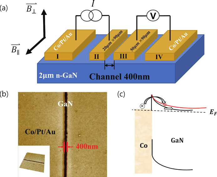
Spin injection and detection in bulk GaN were investigated by performing magnetotransport measurements at low temperatures. A non-local four-terminal lateral spin valve device was fabricated with Co/GaN Schottky contacts. The spin injection efficiency of 21% was achieved at 1.7 K. It was confirmed that the thin Schottky barrier formed between the heavily n-doped GaN and Co was conducive to the direct spin tunneling, by reducing the spin scattering relaxation through the interface states.
GaN spin injection Schottky barrier magnetoresistance Journal of Semiconductors
2023, 44(8): 082501
1 特种环境复合材料技术国家级重点实验室(哈尔滨工业大学), 哈尔滨 150001
2 微系统与微结构制造教育部重点实验室(哈尔滨工业大学), 哈尔滨 150001
5G 通信、能源互联网、新能源汽车、量子技术等高精尖领域对半导体的性能提出了新的更高的要求。第四代半导体金刚石因具有优异的物理化学性能被誉为“终极半导体”, 被认为是制备下一代高功率、高频、高温及低功率损耗电子器件最理想的材料。而浅n型掺杂的技术瓶颈一定程度阻碍了金刚石半导体应用的发展。表面终端研究为金刚石功能化的发展提供了新的策略, 金刚石通过表面终端实现了场效应晶体管、肖特基二极管、日盲紫外探测器、电子发射器件和近表面色心调控等重要应用, 而表面终端发挥作用的机理与其能带结构特点密不可分。本文综述了几种常见终端的能带研究方法, 分析其能带的结构特点, 结合特点介绍其发挥作用的机理, 并进行了总结和展望。
金刚石 表面终端 能带结构 二维空穴气 肖特基结 紫外探测 diamond surface terminal energy band structure two-dimensional hole gas Schottky junction ultraviolet detection


