1 Shanghai Key Laboratory of Modern Optical Systems, Engineering Research Center of Optical Instruments and Systems, Ministry of Education, School of Optical-Electrical and Computer Engineering, University of Shanghai for Science and Technology, Shanghai 200093, China
2 State Key Laboratory of Precision Spectroscopy, East China Normal University, Shanghai 200062, China
3 e-mail: yanliangSPD@163.com
InGaAs/InP avalanche photodiodes typically work in the gated Geiger mode to achieve near-infrared single-photon detection. By using ultrashort gates and combining with the robust spike-canceling technique that consists of the capacitance-balancing and low-pass filtering technique, we demonstrate an InGaAs/InP single-photon detector (SPD) with widely tunable repetition rates in this paper. The operation frequency could be tuned conveniently from 100 MHz to 1.25 GHz with the SPD’s performance measured to maintain good performance, making it quite suitable for quantum key distribution, laser ranging, and optical time domain reflectometry. Furthermore, the SPD exhibited extremely low-noise characteristics. The detection efficiency of this SPD could reach 20% with the dark count rate of 2.5×10⁶/gate and after-pulse probability of 4.1% at 1 GHz.
Shandong Provincial Key Laboratory of Optics and Photonic Device & School of Physics and Electronics, Shandong Normal University, Jinan 250014, China
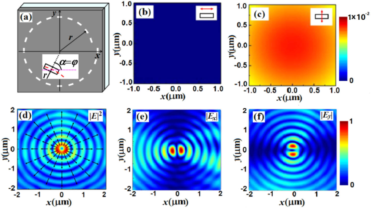
Transmission of an anisotropic metasurface is analyzed in a polar base relying on the Jones calculus, and polarization conversion from the spatial uniform polarization to the spatial nonuniform polarization is explored. Simple and compact polarization converters based on rectangular holes or cross holes etched in silver film are designed, and polarization conversions from the linear and circular polarization to the radial and azimuthal polarization are realized. Numerical simulations of three designed polarization converters consisting of rectangular holes equivalent to polarizers and quarter- and half-wave plates, exhibit the perfect polarization conversion. The experiment results consistent with the simulations verify theoretic predictions. This study is helpful for designing metasurface polarization converters and expanding the application of a metasurface in polarization manipulations.
1 Department of Physics, Baylor University, Waco, Texas 76798, USA
2 The Institute for Quantum Science and Engineering, Texas A&M University, College Station, Texas 77843, USA
3 Princeton University, Princeton, New Jersey 08544, USA
4 e-mail: Scully@tamu.edu
5 e-mail: Zhenrong_Zhang@baylor.edu
Two-dimensional materials are generating great interest due to their unique electrical and optical properties. In particular, transition metal dichalcogenides such as molybdenum disulfide (MoS2) are attractive materials due to the existence of a direct band gap in the monolayer limit that can be used to enhance nonlinear optical phenomena, such as Raman spectroscopy. Here, we have investigated four-wave mixing processes in bulk MoS2 using a multiplex coherent anti-Stokes Raman spectroscopy setup. The observed four-wave mixing signal has a resonance at approximately 680 nm, corresponding to the energy of the A excitonic transition of MoS2. This resonance can be attributed to the increased third-order nonlinear susceptibility at wavelengths near the excitonic transition. This phenomenon could open the path to using MoS2 as a substrate for enhancing four-wave mixing processes such as coherent anti-Stokes Raman spectroscopy.
1 Key Laboratory for Micro/Nano Optoelectronic Devices of Ministry of Education & Hunan Provincial Key Laboratory of Low-Dimensional Structural Physics and Devices, School of Physics and Electronics, Hunan University, Changsha 410082, China
2 e-mail: yanhongzou@hnu.edu.cn
3 e-mail: cjzhao@hnu.edu.cn
Ultrafast fiber lasers are in great demand for various applications, such as optical communication, spectroscopy, biomedical diagnosis, and industrial fabrication. Here, we report the highly stable femtosecond pulse generation from a MXene mode-locked fiber laser. We have prepared the high-quality Ti3C2Tx nanosheets via the etching method, and characterized their ultrafast dynamics and broadband nonlinear optical responses. The obvious intensity- and wavelength-dependent nonlinear responses have been observed and investigated. In addition, a highly stable femtosecond fiber laser with signal-to-noise ratio up to 70.7 dB and central wavelength of 1567.3 nm has been delivered. The study may provide some valuable design guidelines for the development of ultrafast, broadband nonlinear optical modulators, and open new avenues toward advanced photonic devices based on MXenes.
1 Key Laboratory of Radar Imaging and Microwave Photonics, Ministry of Education, Nanjing University of Aeronautics and Astronautics, Nanjing 210016, China
2 e-mail: zhangfangzheng@nuaa.edu.cn
3 e-mail: pans@nuaa.edu.cn
Photonics-based radar with a photonic de-chirp receiver has the advantages of broadband operation and real-time signal processing, but it suffers from interference from image frequencies and other undesired frequency-mixing components, due to single-channel real-valued photonic frequency mixing. In this paper, we propose a photonics-based radar with a photonic frequency-doubling transmitter and a balanced in-phase and quadrature (I/Q) de-chirp receiver. This radar transmits broadband linearly frequency-modulated signals generated by photonic frequency doubling and performs I/Q de-chirping of the radar echoes based on a balanced photonic I/Q frequency mixer, which is realized by applying a 90° optical hybrid followed by balanced photodetectors. The proposed radar has a high range resolution because of the large operation bandwidth and achieves interference-free detection by suppressing the image frequencies and other undesired frequency-mixing components. In the experiment, a photonics-based K-band radar with a bandwidth of 8 GHz is demonstrated. The balanced I/Q de-chirping receiver achieves an image-rejection ratio of over 30 dB and successfully eliminates the interference due to the baseband envelope and the frequency mixing between radar echoes of different targets. In addition, the desired de-chirped signal power is also enhanced with balanced detection. Based on the established photonics-based radar, inverse synthetic aperture radar imaging is also implemented, through which the advantages of the proposed radar are verified.
Key Laboratory of RF Circuits & System of Ministry of Education, Institute of Antennas and Microwave Technology, Hangzhou Dianzi University, Xiasha High Education Park, Hangzhou 310018, China
Magnetic localized surface plasmon modes are supported on metallic spiral structures. Coupling mechanisms for these metamaterial resonators, which are the joint action of magnetic and electric coupling, are studied. Based on the strong coupling, spoof magnetic plasmon modes propagating in the backward direction are proposed along a chain of subwavelength resonators. The theoretical analysis, numerical simulations, and experiments are in good agreement. The proposed novel route for achieving negative-index waveguiding has potential applications in integrated devices and circuits.
1 School of Physics and Optoelectronics Engineering, Xidian University, Xi’an 710071, China
2 CAS Key Laboratory of Standardization and Measurement for Nanotechnology, CAS Center for Excellence in Nanoscience, National Center for Nanoscience and Technology, Beijing 100190, China
3 University of Chinese Academy of Sciences, Beijing 100049, China
4 Graduate Institute of Applied Science and Technology, Taiwan University of Science and Technology, Taipei 106, China
5 Beijing National Laboratory for Condensed Matter Physics, Institute of Physics, Chinese Academy of Sciences, Beijing 100190, China
We report Q-switched and mode-locked erbium-doped all-fiber lasers using ternary ReS2(1x)Se2x as saturable absorbers (SAs). The modulation depth and saturable intensity of the film SA are 1.8% and 0.046MW/cm2. In Q-switched mechanism output, the pulse was centered at 1531.1 nm with maximum pulse energy and minimum pulse width of 28.29 nJ and 1.07 μs, respectively. In mode-locked operation, the pulse was centered at 1561.15 nm with pulse width of 888 fs, repetition rate of 2.95 MHz, and maximum pulse energy of 0.275 nJ. To the best of our knowledge, this is the first report on the mode-locked Er3+-doped fiber laser using ternary transition metal dichalcogenides. This work suggests prospective 2D-material SAs can be widely used in versatile fields due to their attractive optoelectronic and tunable energy bandgap properties.
1 State Key Laboratory of Advanced Optical Communication Systems and Networks, School of Electronics Engineering and Computer Science, Peking University, Beijing 100871, China
2 Peking University Shenzhen Research Institute, Shenzhen 518057, China
An on-chip, high extinction ratio transverse electric (TE)-pass polarizer using a silicon hybrid plasmonic grating is proposed and experimentally demonstrated. Utilizing plasmonics to manipulate the effective index and mode distribution, the transverse magnetic mode is reflected and absorbed, while the TE mode passes through with relatively low propagation loss. For a 6-μm-long device, the measurement result shows that the extinction ratio in the wavelength range of 1.52 to 1.58 μm varies from 24 to 33.7 dB and the insertion loss is 2.8–4.9 dB. Moreover, the structure exhibits large alignment tolerance and is compatible with silicon-on-insulator fabrication technology.
1 Key Laboratory of Space Applied Physics and Chemistry, Ministry of Education, and Shaanxi Key Laboratory of Optical Information Technology, School of Science, Northwestern Polytechnical University, Xi’an 710072, China
2 Department of Electrical and Computer Engineering, National University of Singapore, Singapore 117583, Singapore
3 LEES Program, Singapore-MIT Alliance for Research & Technology (SMART), Singapore 138602, Singapore
Plasmon induced hot electrons have attracted a great deal of interest as a novel route for photodetection and light-energy harvesting. Herein, we report a hot electron photodetector in which a large array of nanocones deposited sequentially with aluminum, titanium dioxide, and gold films can be integrated functionally with nanophotonics and microelectronics. The device exhibits a strong photoelectric response at around 620 nm with a responsivity of 180 μA/W under short-circuit conditions with a significant increase under 1 V reverse bias to 360 μA/W. The increase in responsivity and a red shift in the peak value with increasing bias voltage indicate that the bias causes an increase in the hot electron tunneling effect. Our approach will be advantageous for the implementation of the proposed architecture on a vast variety of integrated optoelectronic devices.
1 State Key Laboratory of Luminescent Materials and Devices, Guangdong Engineering Technology Research and Development Center of Special Optical Fiber Materials and Devices, Guangdong Provincial Key Laboratory of Fiber Laser Materials and Applied Techniques, School of Materials Science and Engineering, South China University of Technology, Guangzhou 510641, China
2 Department of Orthopedics, Zhujiang Hospital, Southern Medical University, Guangzhou 510282, China
3 School of Physics and Physical Engineering, Shandong Provincial Key Laboratory of Laser Polarization and Information Technology, Qufu Normal University, Qufu 273165, China
Bismuth (Bi)-doped photonic materials, which exhibit broadband near-infrared (NIR) luminescence (1000–1600 nm), are evolving into interesting gain media. However, the traditional methods have shown their limitations in enhancing Bi NIR emission, especially in the microregion. Consequently, the typical NIR emission has seldom been achieved in Bi-doped waveguides, which highly restricts the application of Bi-activated materials. Here, superbroadband Bi NIR emission is induced in situ instantly in the grating region by a femtosecond (fs) laser inside borosilicate glasses. A series of structural and spectroscopic characterizations are summoned to probe the generation mechanism. And we show how this novel NIR emission in the grating region can be enhanced significantly and erased reversibly. Furthermore, we successfully demonstrate Bi-activated optical waveguides. These results present new insights into Bi-doped materials and push the development of broadband waveguide amplification.
1 School of Physics and Optoelectronics, South China University of Technology, Guangzhou 510640, China
2 School of Electronic and Information Engineering, South China University of Technology, Guangzhou 510640, China
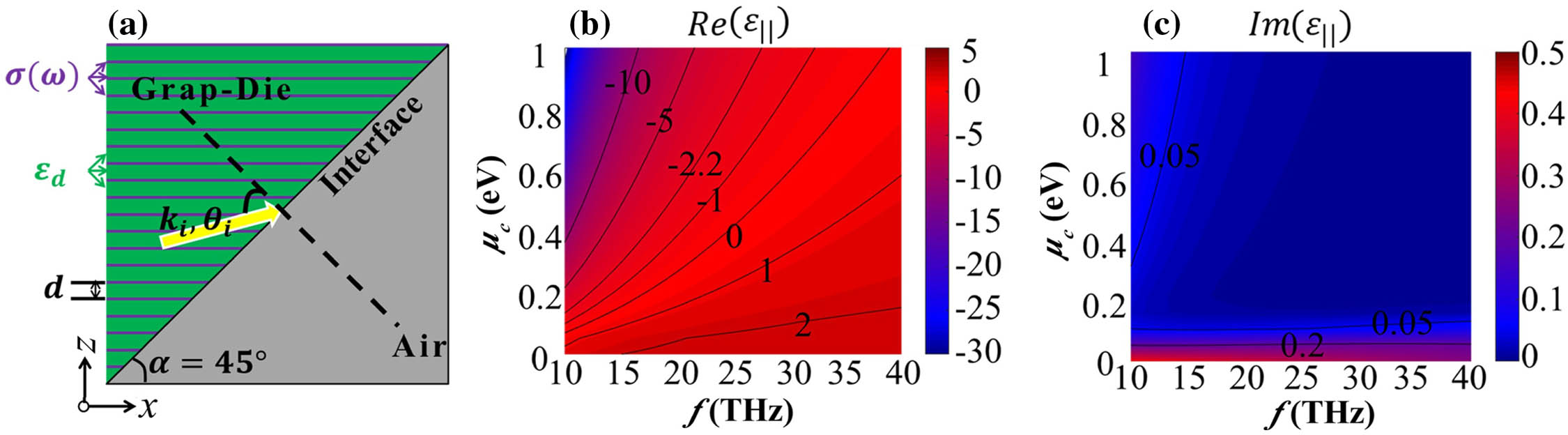
We have studied a switchable hyperbolic metamaterial composed of a graphene–dielectric periodic structure. By tuning the chemical potential of all graphene sheets simultaneously, the isofrequency curve can switch between an ellipse and a hyperbola conveniently. In particular, a special hyperbolic isofrequency curve with its asymptote perpendicular to the interface is obtained and used to realize the zero reflection effect. Furthermore, a zero-reflection-based optical switch working in the terahertz spectrum is demonstrated. Its bandwidth can be efficiently adjusted by geometric parameters such as permittivity and period. Such an optical switch possesses the merits of low loss, high transmittance contrast, high response speed, compact size, high tolerance of chemical potential, and having all incident angles (0°–90°) simultaneously. Such an optical switch holds great potential in many fields, such as data storage, beam steering, and integrated photonic circuits.
1 Institute of Modern Optics, Nankai University, Tianjin 300350, China
2 Tianjin Key Laboratory of Optoelectronic Sensor and Sensing Network Technology, Tianjin 300350, China
3 State Key Laboratory of Applied Optics, Changchun Institute of Optics, Fine Mechanics and Physics, Chinese Academy of Sciences, Changchun 130033, China
4 Nanophotonics and Optoelectronics Research Center, Qian Xuesen Laboratory of Space Technology, China Academy of Space Technology, Beijing 100094, China
5 e-mail: sjchang@nankai.edu.cn
The nonreciprocal circular dichroism and Faraday rotation effect for terahertz (THz) waves in longitudinally magnetized InSb were investigated by theoretical and experimental studies in the THz regime, which indicated its ability for a THz circularly polarized isolator, THz circular polarizer, tunable polarization converter, and polarization modulator by manipulation of different magnetic fields. Furthermore, we demonstrated the InSb plasmonics based on its magneto-optical effects combined with artificial microstructure. We found the magneto-optical enhancement mechanisms in this magneto-plasmonic structure, achieving broadband near-perfect orthogonal linear polarization conversion modulated by the weak magnetic field in an experiment with an extinction ratio of 33 dB. Moreover, the magneto-optical modulation with an amplitude modulation depth of 95.8% can be achieved by this device under a weak magnetic field of 150 mT. InSb and its magneto-plasmonic device have broad potential for a THz isolator, magneto-optical modulator, and polarization convertor in THz application systems.
1 Jiangsu Key Laboratory of Advanced Laser Materials and Devices, Jiangsu Collaborative Innovation Center of Advanced Laser Technology and Emerging Industry, School of Physics and Electronic Engineering, Jiangsu Normal University, Xuzhou 221116, China
2 School of Engineering and Materials Science, Queen Mary University of London, London, UK
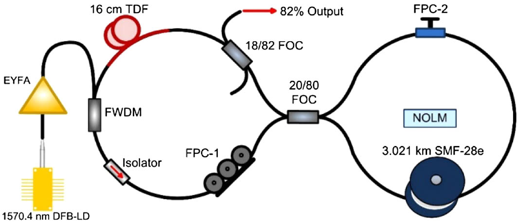
We experimentally demonstrated a type of tunable and switchable harmonic h-shaped pulse generation in a thulium-doped fiber (TDF) laser passively mode locked by using an ultralong nonlinear optical loop mirror. The total cavity length was ~3.03km, the longest ever built for a TDF laser to our best knowledge, which resulted in an ultralarge anomalous dispersion over 200ps2 around the emission wavelength. The produced h-shaped pulse can operate either in a fundamental or in a high-order harmonic mode-locking (HML) state depending on pump power and intra-cavity polarization state (PS). The pulse duration, no matter of the operation state, was tunable with pump power. However, pulse breaking and self-organizing occurred, resulting in high-order HML, when the pump power increased above a threshold. At a fixed pump power, the order of HML was switchable from one to another by manipulating the PS. Switching from the 8th up to the 48th order of HML was achieved with a fixed pump power of ~4.15W. Our results revealed the detailed evolution and switching characteristics of the HML and individual pulse envelope with respect to both the pump power and PS. We have also discussed in detail the mechanisms of both the h-shaped pulse generation and the switching of its HML. This contribution would be helpful for further in-depth study on the underlying dynamics of long-duration particular-envelope pulses with ultralarge anomalous dispersion and ultralong roundtrip time.
Beijing Key Laboratory of Nanophotonics & Ultrafine Optoelectronic Systems, School of Physics, Beijing Institute of Technology, Beijing 100081, China
Entangled photons are the fundamental resource in quantum information processing. How to produce them efficiently has always been a matter of concern. Here we propose a new way to produce correlated photons efficiently from monolayer WS2 based on bound states in the continuum (BICs). The BICs of radiation modes in the monolayer WS2 are realized by designing the photonic crystal slab-WS2-slab structure. The generation efficiency of correlated photon pairs from such a structure has been studied by using a rigorous quantum model of spontaneous parametric down-conversion with the plane wave expansion method. It is found that the generation efficiency of correlated photon pairs is greatly improved if the signal and idler fields are located at the BICs determined by the inverse scattering matrix of the structure. This is in contrast to the parametric down-conversion process for the enhanced generation of nonlinear waves if the pump field is located at the BICs determined by the scattering matrix of the structure. The generation rate of the correlated photon pairs can be improved by 7 orders of magnitude in some designed structures. The generated quantum signals are sensitive to the wavelength and exhibit narrowed relative line width, which is very beneficial for quantum information processing.
1 State Key Laboratory of Silicon Materials and School of Materials Science and Engineering, Zhejiang University, Hangzhou 310027, China
2 e-mail: yuxuegong@zju.edu.cn
3 e-mail: mseyang@zju.edu.cn
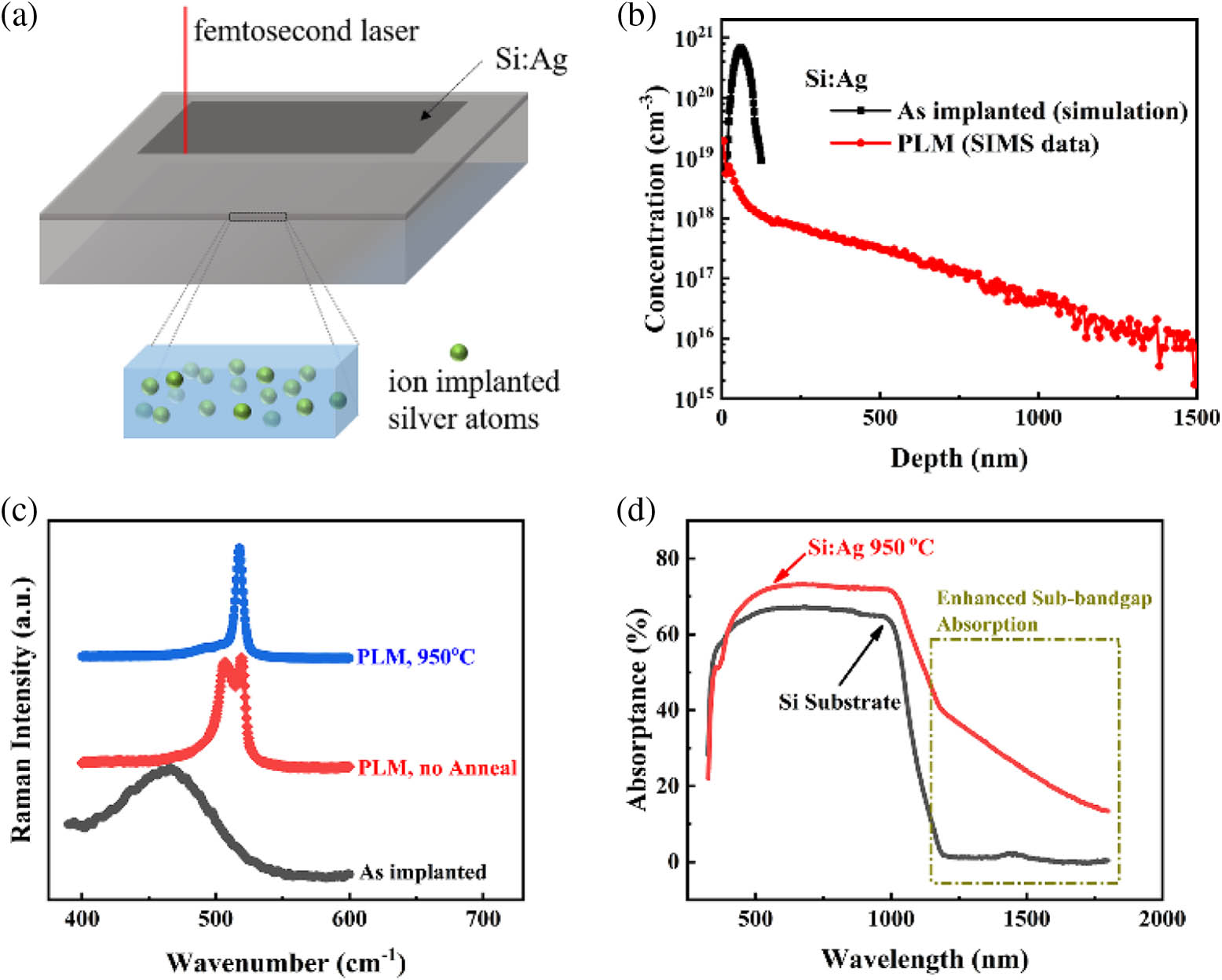
Developing a low-cost, room-temperature operated and complementary metal-oxide-semiconductor (CMOS) compatible visible-blind short-wavelength infrared (SWIR) silicon photodetector is of interest for security, telecommunications, and environmental sensing. Here, we present a silver-supersaturated silicon (Si:Ag)-based photodetector that exhibits a visible-blind and highly enhanced sub-bandgap photoresponse. The visible-blind response is caused by the strong surface-recombination-induced quenching of charge collection for short-wavelength excitation, and the enhanced sub-bandgap response is attributed to the deep-level electron-traps-induced band-bending and two-stage carrier excitation. The responsivity of the Si:Ag photodetector reaches 504mA·W1 at 1310 nm and 65mA·W1 at 1550 nm under 3V bias, which stands on the stage as the highest level in the hyperdoped silicon devices previously reported. The high performance and mechanism understanding clearly demonstrate that the hyperdoped silicon shows great potential for use in optical interconnect and power-monitoring applications.
1 Centre de Nanosciences et de Nanotechnologies, CNRS, Université Paris-Sud, Université Paris-Saclay, C2N—Avenue de la Vauve, 91220 Palaiseau cedex, France
2 Université Paris Lumières, Univ Paris Nanterre, 92410 Ville d’Avray, France
In this paper, we report an experimental demonstration of enabling technology exploiting resonant properties of plasmonic nanoparticles, for the realization of wavelength-sensitive ultra-minituarized (4μm×4μm) optical metadevices. To this end, the example of a 1.3/1.6 μm wavelength demultiplexer is considered. Its technological implementation is based on the integration of gold cut-wire-based metalines on the top of a silicon-on-insulator waveguide. The plasmonic metalines modify locally the effective index of the Si waveguide and thus allow for the implementation of wavelength-dependent optical pathways. The 1.3/1.6 μm wavelength separation with extinction ratio between two demultiplexers’ channels reaching up to 20 dB is experimentally demonstrated. The considered approach, which can be readily adapted to different types of material planar lightwave circuit platforms and nanoresonators, is suited for the implementation of a generic family of wavelength-sensitive guided-wave optical metadevices.
1 Department of Materials Science and Engineering, University of Pennsylvania, Philadelphia, Pennsylvania 19104, USA
2 Department of Electrical and Systems Engineering, University of Pennsylvania, Philadelphia, Pennsylvania 19104, USA
3 Department of Electrical and Computer Engineering, Duke University, Durham, North Carolina 27708, USA
A coherent combination of emission power from an array of coupled semiconductor lasers operating on the same chip is of fundamental and technological importance. In general, the nonlinear competition among the array supermodes can entail incoherence and spectral broadening, leading to a spatiotemporally unstable and multimode emission pattern and thus poor beam quality. Here, by harnessing notions from supersymmetric (SUSY) quantum mechanics, we report that the strategic coupling between a class III-V semiconductor microring laser array with its dissipative superpartner can be used to limit the number of supermodes available for laser actions to one. We introduce a novel approach based on second-order SUSY transformation in order to drastically simplify the superpartner array engineering. Compared to a conventional laser array, which has a multimode spectrum, a SUSY laser array is observed to be capable of operating in a single (transverse) supermode. Enhancement of the peak output intensity of the SUSY laser array has been demonstrated with high efficiency and lower lasing threshold, compared with a single laser and a conventional laser array. Our experimental findings pave the way towards broad-area and high-power light generation in a scalable and stable fashion.
1 State Key Laboratory of Information Photonics and Optical Communications, Beijing University of Posts and Telecommunications, Beijing 100876, China
2 Huawei Technologies Co., Ltd., Shenzhen 518129, China
In this paper, we propose a novel approach to achieve spectrum prediction, parameter fitting, inverse design, and performance optimization for the plasmonic waveguide-coupled with cavities structure (PWCCS) based on artificial neural networks (ANNs). The Fano resonance and plasmon-induced transparency effect originated from the PWCCS have been selected as illustrations to verify the effectiveness of ANNs. We use the genetic algorithm to design the network architecture and select the hyperparameters for ANNs. Once ANNs are trained by using a small sampling of the data generated by the Monte Carlo method, the transmission spectra predicted by the ANNs are quite approximate to the simulated results. The physical mechanisms behind the phenomena are discussed theoretically, and the uncertain parameters in the theoretical models are fitted by utilizing the trained ANNs. More importantly, our results demonstrate that this model-driven method not only realizes the inverse design of the PWCCS with high precision but also optimizes some critical performance metrics for the transmission spectrum. Compared with previous works, we construct a novel model-driven analysis method for the PWCCS that is expected to have significant applications in the device design, performance optimization, variability analysis, defect detection, theoretical modeling, optical interconnects, and so on.


 Download:651次