Ultralow cross talk arrayed waveguide grating integrated with tunable microring filter array
1. Introduction
Wavelength division multiplexing (WDM) is a technique that has been used in many fields of optical communication networks to increase bandwidth and transmission capacity. The silicon (Si)-based WDM has received great attention due to its mature CMOS-compatible process and platform. The Si-based WDM includes Bragg grating[1,2], planar concave grating[3,4], arrayed waveguide grating (AWG)[4–6], Mach–Zehnder interferometers (MZIs)[7–9], and microring resonator (MRR)[10–13]. Among them, AWG is widely used in optical communication systems due to its compact footprint, multiple channels, low insertion loss, etc.
To improve the performance of AWG, many devices with different structures have been designed. The footprint of the devices can be reduced to less than with the design of a reflective structure[14]. The Si AWG can reduce the insertion loss to less than 3 dB while maintaining polarization independence by adjusting the thickness of the top Si layer. However, process errors always affect the actual cross talk of the AWG. To solve this problem, many studies have been validated. One of the effective ways is to fabricate the desired AWG devices on the SiN platform[15]. The relatively low refractive index contrast between SiN waveguides (WGs) and silica cladding layer makes this AWG have a better tolerance for fabrication errors compared with the same condition of an SOI one. However, with a decrease in the relative refractive index contrast, the bending radius of the SiN WGs and the distance between adjacent arrayed WGs must be reconsidered to avoid unnecessary parasitic coupling and insertion loss, which increase the footprint of the device. In our past work, a SiN-Si double-layer folded AWG was designed to ensure device characteristics while reducing the device footprint[16]. However, such a design requires a more complex fabrication process. In addition, some unique structures are designed to solve the cross talk problem of AWG, such as the cascaded AWG structure we designed before[17]. The AWG of this design has a cross talk of and an insertion loss of 3.2 dB, but this design greatly increases the footprint of the device.
In this paper, an AWG combined with a tunable MRR filter is demonstrated to obtain low cross talk while maintaining the device footprint. The tunable MRR filter is carefully designed to match the FSR of the AWG. The insertion loss and cross talk of this design are 3.2 and , respectively. Compared with the normal AWG, the insertion loss of this AWG only increases by approximately 0.5 dB, while the cross talk of this AWG greatly reduces 25 dB. This is a novel scheme for achieving low cross talk AWG on the Si platform.
2. Design and Fabrication
A schematic diagram of both the normal AWG and the designed AWG is presented in Figs. 1(a) and 1(b). As shown in Fig. 1(a), the normal AWG is designed with eight output channels. When an optical signal with a wide spectral range is input into the AWG, it will be divided into eight optical signals with different center wavelengths at the output channel. In Fig. 1(b), the designed AWG can be divided into two parts: the first part remains the same as the normal AWG, while for the second part, a tunable MRR structure with the same design parameters is cascaded in each output channel of the first part. Once an optical signal is coupled to the input channel, the signal with different center wavelengths is divided into eight output channels. At the terminal of each output channel, the signal will be coupled and transferred into the MRR. After filtering by the MRR to reduce cross talk, the signal will finally output from the drop channel of the MRR. In our design, the main structure of the device is one AWG integrated with a tunable MRR resonator array. The fabricated device is shown in Fig. 1(c). In fact, a AWG is designed and fabricated. The first output channel without integrating an MRR is used to more easily align the fiber with the WG, and the multi-input WG is used to compensate the wavelength shift, considering the process deviation. The footprint of the device is mainly determined by the AWG; the footprint of the AWG is , and the footprint of the single MRR is , including the heater and electrode. The main design parameters of the designed AWG are listed in Table 1 (left column). To meet the single-mode condition while reducing the transmission loss, the strip WG is 220 nm in height and 500 nm in width. According to the equation[18], the maximum diffraction order is
Table 1. Design Parameters of the AWG and Ring
| ||||||||||||||||||||||||||||||||||||||||||||||||
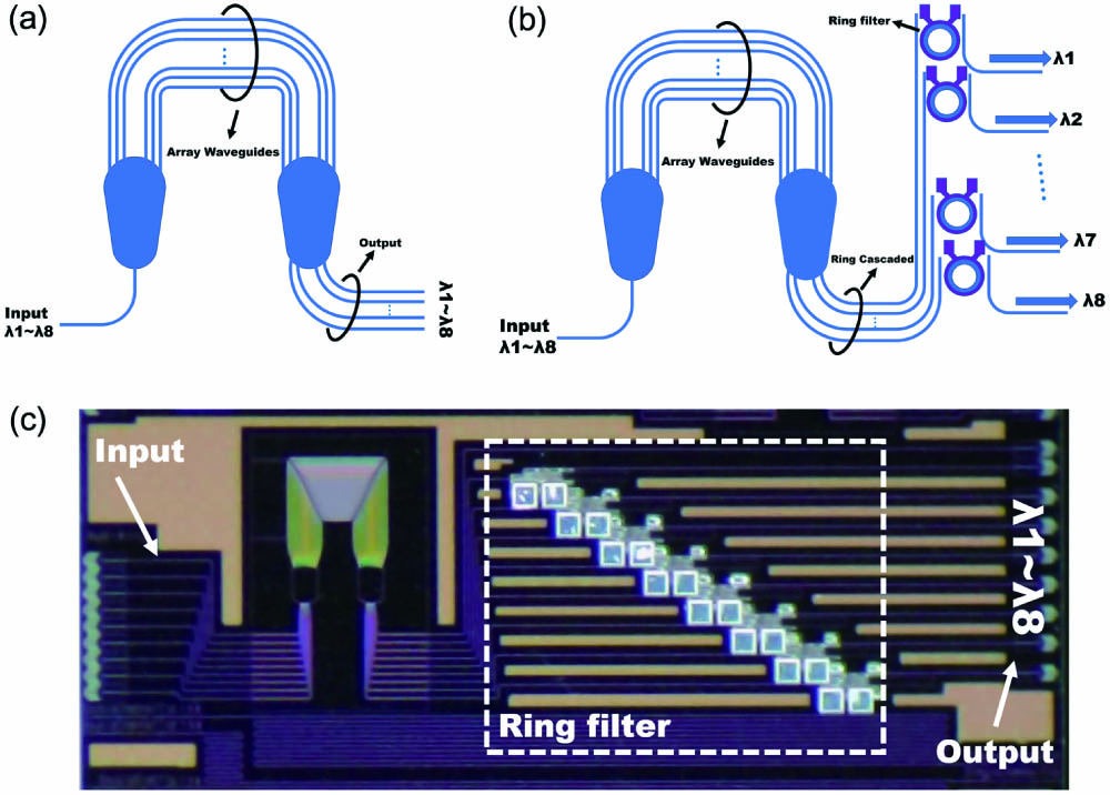
Fig. 1. (a) Schematic diagram of normal AWG; (b) schematic diagram of the designed AWG; (c) optical micrographs of the fabricated ultralow cross talk AWG.
The grating order is chosen as 50, which is equal to . When the channel spacing of 3.2 nm is taken, the length difference was decided to be 23.947 µm between two adjacent arrayed WGs and the radius of the Rowland circle was .
The simulated spectra for the center channel of the AWG with and without MRR are shown in Fig. 2. In our design and simulation, we have optimized factors such as arrayed ridge WGs, bending radius, a bend–straight WG connection, tapers to reduce the phase error from the excitation of higher-order modes, and stray light for lower side lobe of the device. However, according to the requirement of the minimum CD from the FAB, the minimum gap width is 130 nm between two adjacent tapers used to connect the Rowland circle and array WGs. Around 5% of the optical loss is caused by the gap design, which is the main factor of sidelobes in Fig. 2.
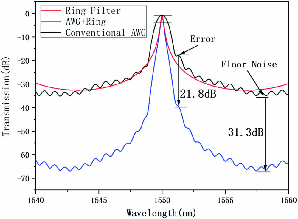
Fig. 2. Simulated transmission spectrum of AWG (with and without errors) and MRR for the central wavelength of 1550 nm.
For this AWG, the sidelobe is approximately . To effectively suppress the appearance of sidelobes, the MRR filters at outputs of AWG are cascaded. It can be seen from Fig. 2 that the sidelobe is reduced by 21.8 dB, and the noise floor of the spectrum is also reduced by 31.3 dB, which greatly improves the performance of the device cross talk. In fact, the MRR filter we designed can also work on AWGs without sidelobes, significantly reducing cross talk.
To implement this theory, we designed and fabricated the device through Singapore AMF. Both the normal and ultralow cross talk AWG were fabricated on the same 8-inch SOI wafer with a 220 nm thick Si layer and a 2 µm buried oxide (BOX). After double lithography/etching processes, the Si WGs were formed. A 1.5 µm cladding layer was deposited by the plasma-enhanced chemical vapor deposition (PECVD) process on the top of the WGs. Then, through PECVD, 100 nm-thick high resistivity TiN was deposited and etched to form heaters above the WG. Afterwards, a 2 µm thickness cladding layer was deposited and etched on the top of TiN metal to form contact holes, and then, a 2 µm-thick Al layer was formed as contact holes above the heater. Finally, to form the air isolation trench, the adjacent and substrate Si layers were etched sequentially.
In our design, the key is to precisely optimize the radius of the MRR. The resonant wavelength of the MRR needs to perfectly match the center wavelength of each channel, especially considering the fabrication tolerance. To achieve this function, TiN heaters are fabricated above the MRRs in our work, and the resonant wavelengths of the MRRs are appropriately tuned to match the central wavelength of each channel through the thermo-optic effect.
The MRR resonance wavelength is very sensitive to the deviation of process. The channel wavelength deviation between AWG and MRR is usually larger when an MRR with a large FSR is chosen. A higher temperature is needed to reduce the wavelength deviation. On the other hand, when FSR is too small, the extinction ratio of the MRR is low and the 3 dB-bandwidth of the MRR is small. Considering the comprehensive performance of the integrated device, the FSR of the MRR is set as 4 times the AWG channel spacing. The schematic illustrating tunable MRR and the optical micrograph of the fabricated MRR are shown in Figs. 3(a) and 3(b). Deep trenches are formed around the device by deep etching to reduce thermal cross talk between the device and adjacent channels; the designed parameters are demonstrated in Table 1 (right column). The bending radius of the MRR can be determined to be 7.6 µm[19] when the central wavelength and .
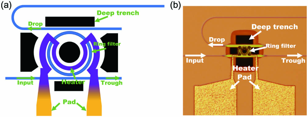
Fig. 3. (a) Schematic illustration of the ring resonator; (b) optical micrograph of the ring resonator.
3. Characterization and Analysis
In the measurements, a wide amplified spontaneous emission source was used to maintain the same polarization over the entire wavelength range. An optical polarization controller (Agilent 8169A), polarizer, and rotatable input fiber were used together to keep the input light in TE mode. The lensed fiber had a spot size of 2.5 µm to couple with the input/output edge coupler of the channel WGs. During the fiber-to-device alignment and test, the output power was detected using a high-sensitivity detector (EXFO CT440). The losses of the straight WG and coupling for the TE mode were achieved by cutting back WGs in the wavelength range.
The spectra of the drop side for both the simulation and actual test are shown in Fig. 4(a). It can be seen from the figure that the actual measured value is consistent with the simulated data. Except for the center resonant wavelength, the shift of the resonance wavelength is expected. TiN heaters on MRRs are designed to address this error due to manufacturing tolerances. The insertion loss of the simulated MRR is 0.1 dB, while the test result is approximately 0.5 dB, which shows that the insertion loss of the AWG will not be significantly increased after cascading the MRR. The modulation depth of both simulated and actual tested MRR exceeds 30 dB, which satisfies the suppression of sidelobes in the AWG. Finally, after our precise design, the measured FSR of the MRR is 12.8 nm, which is 4 times the size of the 3.2 nm channel spacing. Compared with the designed center wavelength of 1550 nm, the 1.9 nm resonance peak wavelength deviation of measured MRR can be eliminated by thermal tuning. This allows the MRR to form a good match with each channel when a voltage is applied. In Fig. 4(b), the current-voltage (I-V) result of the TiN heaters was measured by a Keithley 2450 SourceMeter. The resistivity of the device shows a linear I-V characteristic, and the power consumption is at a voltage of 4 V. To verify the shift of the resonance wavelength under the thermo-optic effect by TiN heaters, different power consumptions are applied from 0 to 120 mW, with a 0.5 V voltage increment. The relation between the resonance peak and applied electric power on the heater of MRR is shown in Fig. 4(c); the turning efficiency is 0.11 nm/mW. When the applied power is 124 mW, the resonance peak at the drop end of the MRR undergoes a redshift of approximately 12.8 nm, which is equal to 1 FSR. When the voltage is swept from 0 to 8.9 V, the MRR can be matched with the center wavelength of all channels. Figure 4(d) red shows the tested shift of the resonance wavelength of an MRR for different times at 7.8 V voltage at a room temperature of 25°C. At the beginning, the resonant wavelength of the MRR slightly shifted to the long wavelength direction. The wavelength shift can be negligible after 1 min. The total shift is only about 0.01 nm before stability, far less than the channel spacing of the AWG. At the same time, the wavelength shift of AWG can be negligible during the bias operation, as shown in black in Fig. 4(d). The isolation structure around the MRR effectively limited the diffusion of the heat. Considering the thermal stability, we started the data collection of the integrated device after the biases were applied for enough time () in our experiment.
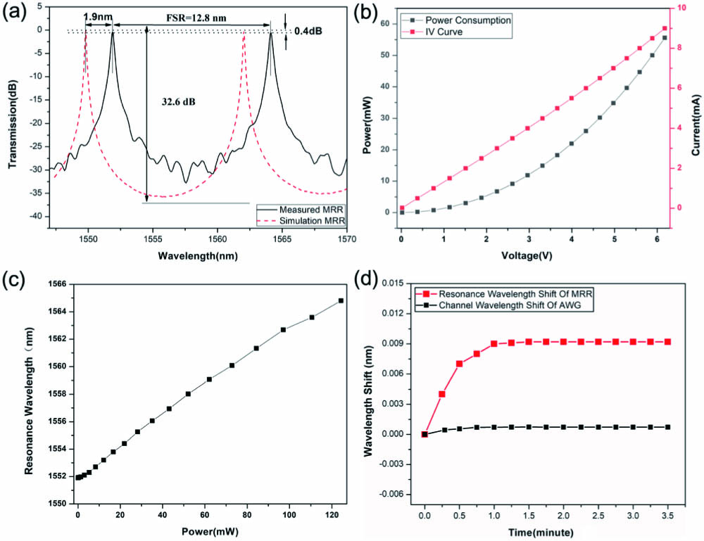
Fig. 4. (a) Transmission spectra of the MRR drop side for both the simulation and actual test; (b) measured I-V curve and power consumption of the MRR; (c) relation between resonance wavelength and applied electric power on the heater of MRR; (d) shift of the resonance wavelength of MRR under 7.8 V voltage (red) and wavelength shift of the AWG first channel under voltage application (black).
During the integrated device testing, the input light is coupled into the device from the fifth input WG of the AWG. To ensure that the resonance peak of the MRR can be tuned to match the resonance peak with the center wavelength of each channel of the AWG, various voltages are applied to each MRR; the applied voltage is shown in Table 2. The deviation between the resonance wavelength of the ring and center wavelength of each channel in the AWG is in the range of 0.03 to 0.06 nm with the bias. The output spectra of both the normal AWG and the ultralow cross talk AWG are shown in Figs. 5(a) and 5(b). As seen from the figure, the on-chip loss of the ultralow cross talk AWG is , which is higher than the loss of a normal AWG. The excess loss is mainly from the ring filter, which is consistent with the previous test of the independent MRR. The measured nonuniformity performance of the ultralow cross talk AWG is 1.34 dB, which is similar to and better than that of the reference AWG, 1.61 dB. In Fig. 5(b), the measured adjacent cross talk is from to for eight channels of the integrated device. Compared to a conventional AWG, the adjacent cross talk is lower than 19.9 dB by the double-filtering structure. Compared to a normal AWG, the noise floor of the spectrum is also reduced by , which is consistent with the simulated data. The center wavelength of output channel 4 is 1549.75 nm, which has a shift of 0.25 nm compared with the 1550 nm design. The wavelength shift is mainly caused by the top Si thickness deviation of the commercial SOI wafer, the width deviation of the processed WG. These factors will cause the deviation of the effective refractive index of the arrayed WGs and make the central wavelength shift. In our design and measurement, the room temperature is set, so this shift can be negligible.
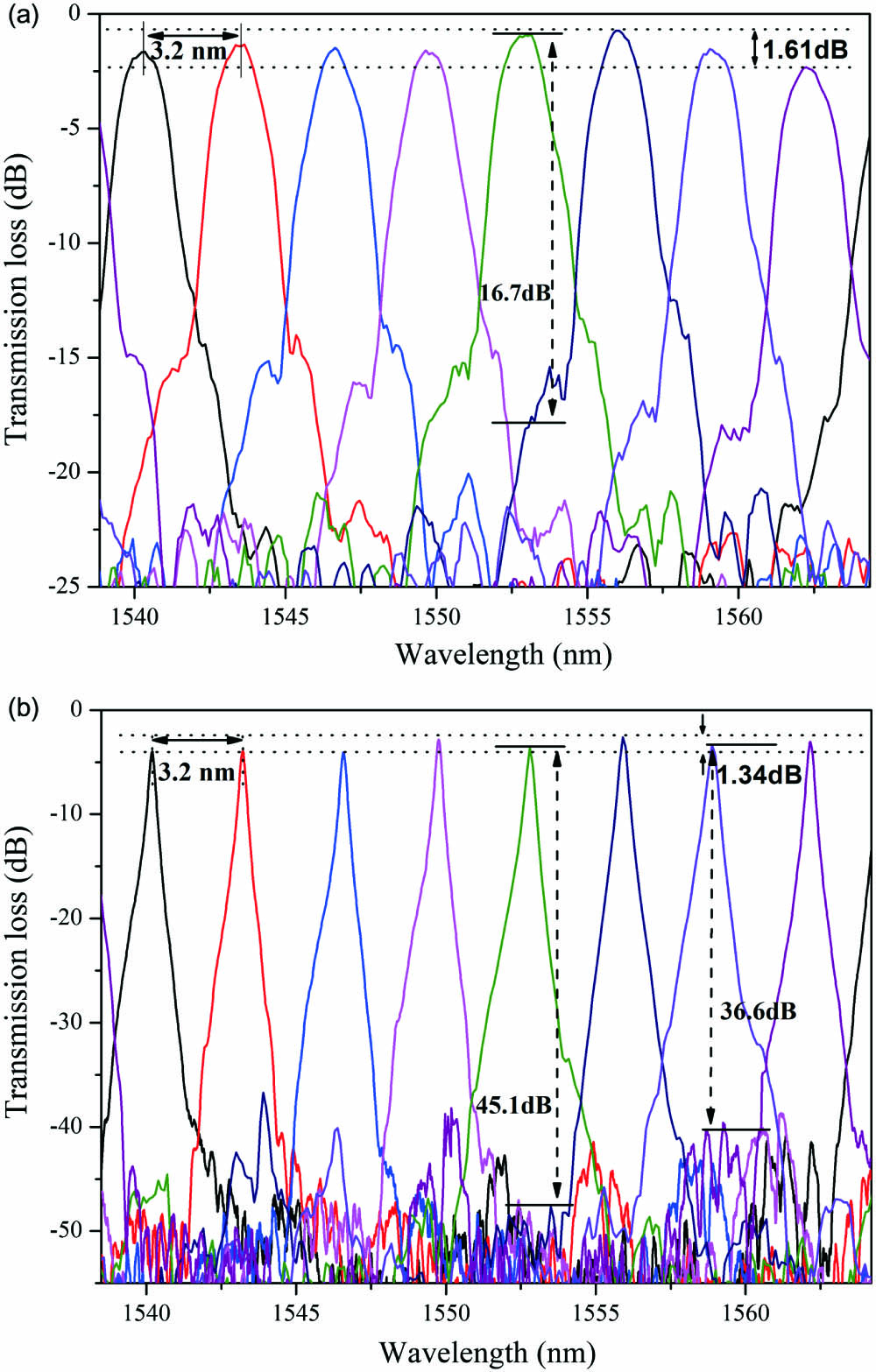
Fig. 5. Measured spectra of AWG. (a) Reference normal AWG; (b) ultralow cross talk AWG integrated with MRRs.
Table 2. Various Voltages Applied on the MRR to Overlap with the Center Wavelength of Each Channel of the AWG
|
4. Conclusion
An ultralow cross talk AWG via a tunable MRR filter is demonstrated on the SOI platform. A tunable MRR is integrated into each output channel of the normal AWG. The cross talk caused by processing and design errors can be effectively optimized by the combination of this structure. The measured insertion loss and adjacent cross talk of the designed AWG are approximately 3.2 and , respectively. Compared with the single AWG or cascaded microring wavelength division multiplexer design, the integration of the MRR filter can greatly promote the cross talk of AWG with the standard CMOS process. In order to improve the limited bandwidth, using cascaded multi MRRs replacing a single MRR should be a good solution. The next step will be to design a large-bandwidth AWG and integrate a flat-spectrum dual MRR filter.
Article Outline
Heming Hu, Shiping Liu, Tianwen Li, Yongjie Fan, Hua Chen, Qing Fang. Ultralow cross talk arrayed waveguide grating integrated with tunable microring filter array[J]. Chinese Optics Letters, 2024, 22(3): 031303.
