可调谐四宽带太赫兹吸收器设计【增强内容出版】
Since the first metamaterial perfect absorber was proposed by Landy et al., it has been widely developed due to its potential applications in the fields of microwave radiation measurement, biosensors, thermal emitters, and imaging. Many existing absorbers face the issue of narrow bandwidths, which fail to satisfy the demands of some optoelectronic devices. To solve this problem, it is common to construct different patterns in the same layer or stack multilayer structures with different geometrical dimensions. However, these structures are often complex, and the absorption rate cannot be actively adjusted. Therefore, phase change materials have been introduced to regulate the absorption rate of absorbents, and vanadium dioxide is one of them. There are many absorbers designed with VO2, but the absorption bandwidth and band number need to be further increased. Therefore, combining the characteristics of multi-band, wideband, and tunable absorption remains a meaningful endeavor.
To effectively study the performance of the absorber, the proposed structure is analyzed by using the microwave simulation software CST Microwave Studio 2020. The metamaterial absorber in this study consists of three layers: the top layer VO2, the middle layer SiO2, and the bottom layer Au. When the conductivity is adjusted from 200 S/m to 2×10⁵ S/m, VO2 will change from an insulator to metal, which can be simulated by input conductivity parameters through the Drude model in CST software. The absorber's absorption can be obtained through one minus the reflection and transmission. Since the penetration depth of the incident wave is smaller than the Au thickness, thus the transmittance is zero. Perfect absorption can be achieved when the reflection is also zero. Material selection and structural design are used to achieve impedance matching, ensuring zero reflection and ultimately realizing perfect absorption of multiple broadbands.
The simulation results show that there are four absorption bands with more than 90% of absorptivity in the range of 0-10 THz, covering bandwidths of 0.87, 0.58, 0.61, and 0.45 THz, respectively. With variations in the conductivity of VO2, the absorptivity dynamically adjusts between 7.7% and 99.9% (Fig. 2). The analysis finds that with the change of dielectric constant of vanadium dioxide, the resonant frequency remains almost constant, while the absorption rate changes significantly. The Fabry-Perot resonance theory and impedance matching theory are introduced to explain the effects of the dielectric layer and the VO2 layer on the absorption (Figs. 3-5). The physical sources of multiple perfect absorption peaks are analyzed through the electric field distribution (Fig. 6). Additionally, changes in absorptivity with different incident angles and polarization angles are analyzed (Fig. 7), which shows that the absorber has the characteristics of polarization insensitivity and wide-angle absorption.
We describe a terahertz absorber with four absorption bands, dynamically adjustable absorptivity, and a simple structure. Simulation results indicate that within the range of 0-10 THz, there are four absorption bands with more than 90% absorptivity, and their respective bandwidths are 0.87, 0.58, 0.61, and 0.45 THz. The absorptivity can be dynamically adjusted between 7.7% and 99.9% by varying the conductivity of vanadium dioxide. The physical mechanism of the absorber is explained using impedance matching theory and Fabry-Perot resonance theory. Through the analysis of the electric field distribution, it is found that the first broadband absorption is mainly caused by the local absorption of VO2, while the second, third, and fourth broadband absorptions result from the resonance absorption of multiple electric dipoles on the surface of VO2, coupled with the coupling effects between the dielectric layer and VO2 and the metal layer. Additionally, it has the features of wide-angle absorption and polarization insensitivity. This absorber has potential applications in micro-radiometers, biosensors, stealth technology, and other fields.
1 引言
电磁超材料是利用现有材料人工设计成的单元结构,具有一些超越自然性质的特性。自从负折射率材料[1]、金属线组成的超材料[2-4]被提出后,超材料受到科学界的广泛关注。超材料在很多领域得到发展应用,比如完美吸收器[5-7]、光学透镜[8-9]和隐形斗篷[10-11]等。其中,自从第一个超材料完美吸收器(MPA)被Landy等[12]提出后,MPA在微波辐射计[13-15]、生物传感器[16-17]、热辐射器[18-19]和成像[20]等领域的应用范围迅速扩大。
这些MPA大部分是单频点或者多频点的,例如张晓健等[21]设计的两频点吸收器、张向等[22]设计的具有4个频点的吸收器,这些吸收器都存在频带窄的问题,不能满足某些光电器件的需求。为了解决此问题,通常采用在同一层单元中构造不同图形,或者不同图形多层叠加的结构。然而,这些结构往往比较复杂,且存在吸收率不能主动调节的问题。近年来,超材料设计中引用了各种可变材料[23-28],从而使这些器件的光学性能能够被主动控制。二氧化钒(VO2)就是一种可控的功能材料,它可以被热、电或光[29]激发,实现从绝缘状态到金属状态的变换。近期,很多学者报道了使用VO2设计的宽带MPA,例如:Song等[30]提出一种吸收率变化范围为30%~100%的宽带吸收器,其中吸收率大于90%的带宽为0.33 THz;Hu等[31]提出一种双宽带吸收器,95%以上吸收率的带宽为0.5 THz和0.6 THz。Huang等[32]设计了一种80%以上吸收率的带宽分别为0.88 THz和0.77 THz的双宽带吸收器。但是,这些MPA均存在频带较窄或频带数量较少的问题。
根据多个尺寸吸收器叠加的逻辑,可以获得很多吸收带,但实际上,由4个不同大小的谐振器组成的超级谐振器[33],相邻谐振器的相互作用非常大,要想利用不同尺寸的谐振器实现4个频带以上的超级谐振器是非常困难的。令人欣慰的是,最近一些小组的研究同时激发了基模和高阶模态共振,如环形矩形腔[34]、多层光栅[35]等,但是利用高阶模态所激发的吸收率一般小于50%。可见,综合优化多频带、宽带和可调谐这3个特性仍是一项很有意义的工作。
本文提出一种在0~10 THz内具有4个宽带的太赫兹吸收器,其结构较为简单。随着温度或者光照变化,所提吸收器的吸收率在7.7%~99.9%内动态可调。讨论了吸收器的顶层和中间介质层变化对吸收器性能的影响,分析了4个吸收峰的机理和来源,并分析了极化角和入射角对吸收性能的影响。本研究可以在一定程度上促进生物传感器、光电器件等太赫兹器件的应用。
2 结构模型和方法
所设计的超材料吸收器为三层结构,上层是VO2层,中间层是二氧化硅(SiO2)层,下层是金(Au)接地层,

图 1. 宽带吸收器结构图。(a)整个阵列图;(b)单个单元顶视图
Fig. 1. Diagram of broadband absorb structure. (a) Schematic of complete array; (b) top view of unit
为了有效研究吸收器的性能,采用基于有限积分技术的微波仿真软件CST Microwave Studio 2020对所提结构进行仿真。VO2的光学性能可以由Drude模型[36-37]描述,即
式中:
之前的研究表明,当温度从298 K(室温)增加到340 K时,VO2会从绝缘态转变为金属态,其电导率可以从200 S/m调整到2×105 S/m[38-39]。
吸收器的吸收率
3 分析与讨论
3.1 结果分析
如
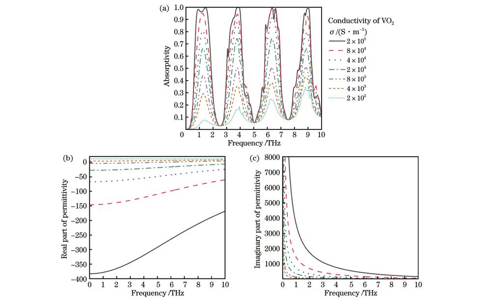
图 2. 吸收率、介电常数实部和虚部随VO2电导率的变化。(a)吸收率随VO2电导率的变化;(b)介电常数实部随VO2电导率的变化;(c)介电常数虚部随VO2电导率的变化
Fig. 2. Absorption and real part and imaginary part of the permittivity with different conductivities of VO2. (a) Absorption with different conductivities of VO2; (b) real part of permittivity with different conductivities of VO2; (c) imaginary part of permittivity with different conductivities of VO2
3.2 介质层和顶层分析
研究了介质层SiO2和顶层VO2对吸收性能的影响。
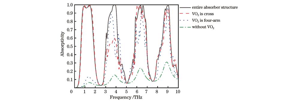
图 3. 去掉VO2、VO2为四臂形、VO2为十字形以及完整吸收结构的吸收曲线
Fig. 3. Absorption curves of without VO2, VO2 is cross, VO2 is four-arm, and entire absorber structure
在顶层设计了VO2图形结构。如

图 4. 吸收光谱随SiO2厚度及损耗正切值的变化。(a)吸收光谱随SiO2厚度变化;(b)吸收光谱随SiO2损耗正切值变化
Fig. 4. Absorption spectra under different thicknesses and tangent losses of SiO2. (a) Absorption spectra under different thicknesses of SiO2; (b) absorption spectra under different tangent losses of SiO2
3.3 完美吸收机理
该设计的完美吸收基于阻抗匹配理论[42-43]。吸收率和相对阻抗之间的关系为
式中:Z为吸收器的阻抗;
由

图 5. 吸收器相对阻抗随电导率的变化。(a)相对阻抗的实部;(b)相对阻抗的虚部
Fig. 5. Relative impedance at different VO2 conductivities. (a) Real part of relative impedance; (b) imaginary part of relative impedance
为了进一步了解宽带吸收的物理来源,
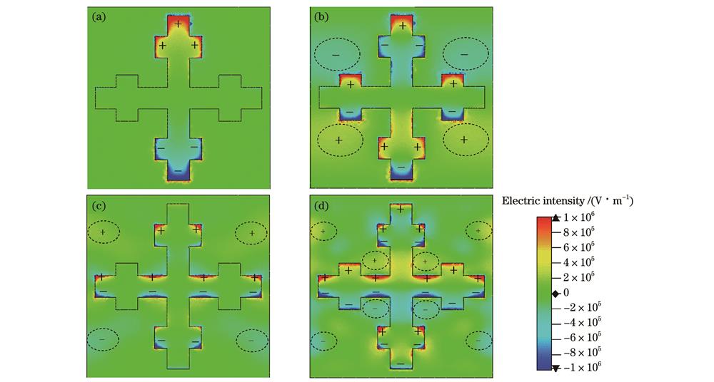
图 6. 4个吸收峰的表面电场分布。(a)f1=1.44 THz;(b)f2=3.89 THz;(c)f3=6.63 THz;(d)f4=9.03 THz
Fig. 6. Surface electric field distribution at four absorption peaks. (a) f1=1.44 THz; (b) f2=3.89 THz; (c) f3=6.63 THz; (d) f4=9.03 THz
3.4 广角吸收及偏振不敏感
不同极化角和入射角下吸收器吸收率的变化如

图 7. 入射角和偏振角对吸收的影响。(a)TE模式入射角的影响;(b)TM模式入射角的影响;(c)TE模式极化角的影响
Fig. 7. Effect of incidence and polarization angles on absorption. (a) Effect of incidence angle in TE mode; (b) effect of incidence angle in TM mode; (c) effect of polarization angle in TE mode
4 结论
提出一种多宽带、吸收主动可调的宽带吸收器,其由MPA的三层结构组成。结果表明,吸收率超过90%的宽带共有4个,带宽分别为0.87、0.58、0.61、0.45 THz。通过使用热控制来诱导VO2电导率变化,吸收器的吸收率可从7.7%动态调整到99.9%。为了解释所设计吸收器的物理机理,引入了法布里-珀罗共振和阻抗匹配理论。通过对电场分布的分析发现,第一个宽带主要是由VO2的局部吸收引起的,第二~四宽带的形成除了有VO2表面多个电偶极子共振吸收外,还有介质层与VO2和金属层之间的耦合效应所引起的吸收。此外,所设计的吸收器具有极化不敏感特性和良好的广角吸收性能,在成像、调制、传感和隐身方面有很大的应用潜力。
[1] Shelby R A, Smith D R, Schultz S. Experimental verification of a negative index of refraction[J]. Science, 2001, 292(5514): 77-79.
[2] Yuan Y, Bingham C, Tyler T, et al. A dual-resonant terahertz metamaterial based on single-particle electric-field-coupled resonators[J]. Applied Physics Letters, 2008, 93(19): 191110.
[3] Ogando K, Pastoriza H. Design of integration-ready metasurface-based infrared absorbers[J]. Journal of Applied Physics, 2015, 118(4): 043109.
[4] Wu K M, Huang Y J, Wang H T L, et al. Numerical and theoretical analysis on the absorption properties of metasurface-based terahertz absorbers with different thicknesses[J]. Applied Optics, 2015, 54(2): 299-305.
[5] Bao Z Y, Wang J C, Hu Z D, et al. Coordinated multi-band angle insensitive selection absorber based on graphene metamaterials[J]. Optics Express, 2019, 27(22): 31435-31445.
[6] Bao Z Y, Wang J C, Hu Z D, et al. Coordination multi-band absorbers with patterned irrelevant graphene patches based on multi-layer film structures[J]. Journal of Physics D, 2021, 54(50): 505306.
[8] Pendry J B. Negative refraction makes a perfect lens[J]. Physical Review Letters, 2000, 85(18): 3966-3969.
[9] 唐剑雄, 龚岩栋, 庞恺. 二维超构表面:超透镜应用及研究进展[J]. 激光与光电子学进展, 2023, 60(21): 2100004.
[10] Bilotti F, Tricarico S, Vegni L. Plasmonic metamaterial cloaking at optical frequencies[J]. IEEE Transactions on Nanotechnology, 2010, 9(1): 55-61.
[11] Schurig D, Mock J J, Justice B J, et al. Metamaterial electromagnetic cloak at microwave frequencies[J]. Science, 2006, 314(5801): 977-980.
[12] Landy N I, Sajuyigbe S, Mock J J, et al. Perfect metamaterial absorber[J]. Physical Review Letters, 2008, 100(20): 207402.
[14] Maier T, Brueckl H. Multispectral microbolometers for the midinfrared[J]. Optics Letters, 2010, 35(22): 3766-3768.
[15] Grant J, Escorcia-Carranza I, Li C, et al. A monolithic resonant terahertz sensor element comprising a metamaterial absorber and micro-bolometer[J]. Laser & Photonics Reviews, 2013, 7(6): 1043-1048.
[17] Li R F, Wu D, Liu Y M, et al. Infrared plasmonic refractive index sensor with ultra-high figure of merit based on the optimized all-metal grating[J]. Nanoscale Research Letters, 2017, 12(1): 1.
[18] Karalis A, Joannopoulos J D. 'Squeezing' near-field thermal emission for ultra-efficient high-power thermophotovoltaic conversion[J]. Scientific Reports, 2016, 6: 28472.
[19] Xiao D, Tao K Y. Ultra-compact metamaterial absorber for multiband light absorption at mid-infrared frequencies[J]. Applied Physics Express, 2015, 8(10): 102001.
[20] Ouchi T, Kajiki K, Koizumi T, et al. Terahertz imaging system for medical applications and related high efficiency terahertz devices[J]. Journal of Infrared, Millimeter, and Terahertz Waves, 2014, 35(1): 118-130.
[21] 张晓健, 张权, 兰桂莲, 等. 基于塔姆等离激元的硼烯近完美吸收器[J]. 光子学报, 2023, 52(10): 1052404.
[22] 张向, 王玥, 张婉莹, 等. 单壁碳纳米管太赫兹超表面窄带吸收及其传感特性研究[J]. 物理学报, 2024, 73(2): 026102.
Zhang X, Wang Y, Zhang W Y, et al. Narrow band absorption and sensing properties of the THz metasurface based on single-walled carbon nanotubes[J]. Acta Physica Sinica, 2024, 73(2): 026102.
[23] Shin J H, Park K H, Ryu H C. Electrically controllable terahertz square-loop metamaterial based on VO2 thin film[J]. Nanotechnology, 2016, 27(19): 195202.
[24] Xu Z H, Wu D, Liu Y M, et al. Design of a tunable ultra-broadband terahertz absorber based on multiple layers of graphene ribbons[J]. Nanoscale Research Letters, 2018, 13(1): 143.
[25] Zhai Z C, Zhang L, Li X J, et al. Tunable terahertz broadband absorber based on a composite structure of graphene multilayer and silicon strip array[J]. Optics Communications, 2019, 431: 199-202.
[26] 朱华利, 张勇, 叶龙芳, 等. 基于石墨烯-二氧化钒的太赫兹双控可调宽带吸收器[J]. 光学学报, 2022, 42(14): 1423002.
[27] Song Z Y, Wang Z S, Wei M L. Broadband tunable absorber for terahertz waves based on isotropic silicon metasurfaces[J]. Materials Letters, 2019, 234: 138-141.
[28] 陈宇婷, 薛文瑞, 张敬, 等. 基于二氧化钒的动态可调谐的红外线超宽带吸收器[J]. 中国激光, 2023, 50(19): 1913001.
[29] Jepsen P U, Fischer B M, Thoman A, et al. Metal-insulator phase transition in a VO2 thin film observed with terahertz spectroscopy[J]. Physical Review B, 2006, 74(20): 205103.
[30] Song Z Y, Wang K, Li J W, et al. Broadband tunable terahertz absorber based on vanadium dioxide metamaterials[J]. Optics Express, 2018, 26(6): 7148-7154.
[31] Hu N, Wu F L, Bian L A, et al. Dual broadband absorber based on graphene metamaterial in the terahertz range[J]. Optical Materials Express, 2018, 8(12): 3899-3909.
[32] Huang J, Li J N, Yang Y, et al. Active controllable dual broadband terahertz absorber based on hybrid metamaterials with vanadium dioxide[J]. Optics Express, 2020, 28(5): 7018-7027.
[33] Wang B X, Zhai X, Wang G Z, et al. Design of a four-band and polarization-insensitive terahertz metamaterial absorber[J]. IEEE Photonics Journal, 2015, 7(1): 4600108.
[34] Dayal G, Solanki A, Chin X Y, et al. High-Q plasmonic infrared absorber for sensing of molecular resonances in hybrid lead halide perovskites[J]. Journal of Applied Physics, 2017, 122(7): 073101.
[35] Liu X Y, Gao J S, Yang H G, et al. Multiple infrared bands absorber based on multilayer gratings[J]. Optics Communications, 2018, 410: 438-442.
[36] Bai J J, Zhang S S, Fan F, et al. Tunable broadband THz absorber using vanadium dioxide metamaterials[J]. Optics Communications, 2019, 452: 292-295.
[37] Wang T L, Zhang Y P, Zhang H Y, et al. Dual-controlled switchable broadband terahertz absorber based on a graphene-vanadium dioxide metamaterial[J]. Optical Materials Express, 2020, 10(2): 369-386.
[38] Lian Y, Li Y K, Lou Y P, et al. Adjustable trifunctional mid-infrared metamaterial absorber based on phase transition material VO2[J]. Nanomaterials, 2023, 13(12): 1829.
[39] 王岩, 陈哲, 崔琦. 基于二氧化钒的可调谐太赫兹宽带带通滤波器[J]. 光学学报, 2021, 41(20): 2023002.
[40] Song Z Y, Wei M L, Wang Z S, et al. Terahertz absorber with reconfigurable bandwidth based on isotropic vanadium dioxide metasurfaces[J]. IEEE Photonics Journal, 2019, 11(2): 4600607.
[41] Zhao Z Y, Zhao H W, Peng W, et al. Polarization dependence of terahertz Fabry-Pérot resonance in flexible complementary metamaterials[J]. Plasmonics, 2015, 10(6): 1587-1592.
[42] Zhao Y, Huang Q P, Cai H L, et al. A broadband and switchable VO2-based perfect absorber at the THz frequency[J]. Optics Communications, 2018, 426: 443-449.
[43] 樊浩田, 薛文瑞, 陈宇婷, 等. 基于金属铑和二氧化硅材料的紫外线超宽带吸收器[J]. 中国激光, 2024, 51(2): 0213003.
[44] Zhao L, Liu H, He Z H, et al. Theoretical design of twelve-band infrared metamaterial perfect absorber by combining the dipole, quadrupole, and octopole plasmon resonance modes of four different ring-strip resonators[J]. Optics Express, 2018, 26(10): 12838-12851.
[45] Wang J C, Wang X Y, Hu Z D, et al. Independent tunable multi-band absorbers based on molybdenum disulfide metasurfaces[J]. Physical Chemistry Chemical Physics, 2019, 21(43): 24132-24138.
[46] Zhu B, Wang Z B, Huang C, et al. Polarization insensitive metamaterial absorber with wide incident angle[J]. Progress in Electromagnetics Research, 2010, 101: 231-239.
张婷, 郭泰铭, 闫俊伢, 裴娅男. 可调谐四宽带太赫兹吸收器设计[J]. 光学学报, 2024, 44(5): 0523002. Ting Zhang, Taiming Guo, Junya Yan, Yanan Pei. Design of Tunable Four-Broadband Terahertz Absorber[J]. Acta Optica Sinica, 2024, 44(5): 0523002.
