高光束质量大功率垂直腔面发射激光器封面文章
Compared with edge-emitting lasers, vertical-cavity surface-emitting lasers (VCSELs) have superior performance, such as a lower threshold current, single longitudinal-mode output, easy 2D array integration, low power consumption, and low fabrication cost. With the development of large apertures as well as 2D arrays of VCSELs, the output power of VCSELs has been significantly improved, and they are widely used in such fields as optical communication, optical interconnection, and optical information processing. In addition, the applications of VCSEL devices in the consumer field are becoming increasingly extensive, such as LiDAR, distance sensing, autofocusing, 3D sensing, rainbow-mode recognition, air and water quality detection, and virtual reality (VR)/augmented reality (AR)/mixed reality (MR). In recent years, the performances of VCSELs in terms of output power, conversion efficiency, modulation bandwidth, and reliability have improved continuously. However, high-power VCSEL single-tube or array devices are mostly multi-transverse-mode outputs, resulting in poor output beam quality. Therefore, improving device power while obtaining better beam quality in the optical field is a technical challenge that current researchers must solve. In this study, a novel multi-ring cavity structure is used to integrate VCSEL arrays to obtain a better far-field distribution while maintaining a high power output, further expanding the application range of VCSELs in the field of smart devices.
In this study, by analyzing the reasons for the non-uniform carrier distribution of large-aperture VCSELs, a multi-annular cavity structure [Fig. 2(b)] is designed to separate the injected current region into multiple regions to suppress the carrier aggregation effect. The finite-different time-domain (FDTD) method is used for the simulation to optimize the optical field distribution by adjusting the size of the annular cavities and the percentage of the light-out region. On this basis, traditional and new-structure VCSELs with identical external diameters of light exit holes are prepared on the same epitaxial wafer, and their light field uniformity and output characteristics are compared and analyzed.
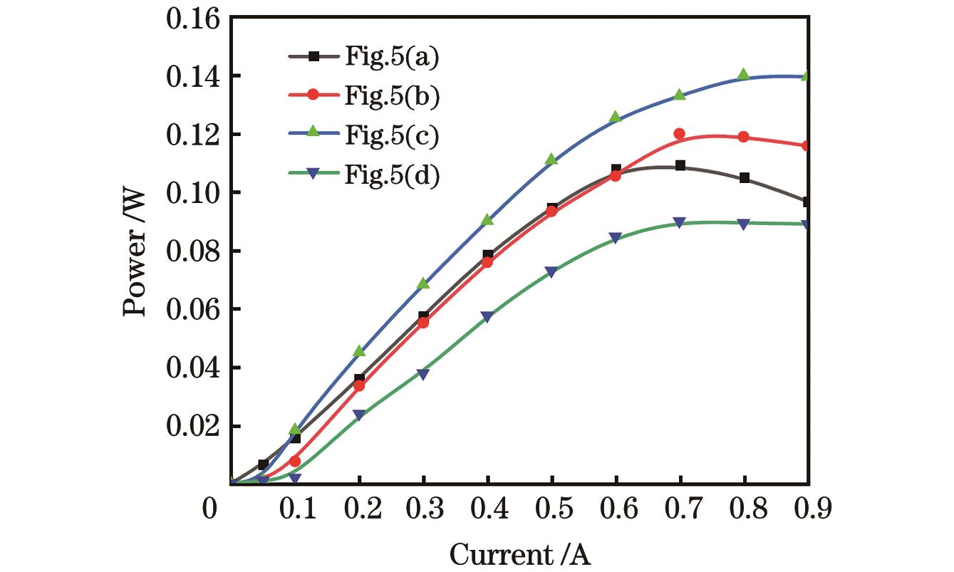
Near-field photographs of conventional and novel-structure VCSELs tested under the same injection conditions are taken (Fig. 5). The test results show that the light field distribution uniformity of the conventional VCSEL structure [Fig. 5(d)] is extremely poor, and only the annular region near the electrode ring emits light. In contrast, the three ring-cavity structures (A, B, and C) are fully illuminated in all light-emitting regions and have a more uniform light field distribution, which significantly improves the extremely poor light field distribution of the conventional structure owing to the carrier aggregation and space-burning hole effects. By comparison, it can be seen that the structure C not only has better light field uniformity and high utilization of the light-emitting region but, more importantly, has the strongest light field, which is consistent with the theoretical simulation results. In addition, as can be seen from the far-field distribution and spectrogram of the VCSEL with structure C (Fig. 6), the optical field center of the far field has a strong intensity, showing a Gaussian distribution, and the excitation spectrum verifies its excellent single-mode characteristics, with a peak wavelength of 805.03 nm and a spectral full width at half-maximum of 0.82 nm. The device exhibits a very good excitation characteristic. In addition, the conventional VCSEL structure (Fig. 8) has a maximum continuous output power of 90 mW at 0.7 A and a threshold current of 80 mA. The output power and slope efficiency of the new structure are improved compared with those of the traditional-structure device, and the threshold current is reduced. The threshold current of new structure C is 49 mA, and the maximum continuous output power is 140 mW, which is nearly 56% higher than that of the conventional structure.
In this study, by analyzing the reasons for the uneven carrier distribution of large-aperture VCSELs, a multi-annular-cavity-structured VCSEL is designed, and the optical field of the new structure is simulated. The results show that the optical field distribution can be optimized by optimizing the dimensions of the annular cavities and the percentage of the light-output region. Based on this, traditional and new-structured VCSELs with identical external diameters of light exit holes are prepared on the same epitaxial wafer, and the light field uniformity and output characteristics of the new structure are compared and analyzed. The results show that the new structure improves the uneven distribution of the light field caused by the carrier aggregation effect of the traditional structure. The new multi-ring cavity structured VCSEL with a 67% duty cycle has the best near-field distribution, and the threshold current is reduced. On applying an injection current of 0.8 A, the continuous output power at room temperature reaches 140 mW, which is 56% higher than that obtained with the traditional structure, and the far-field shows a Gaussian distribution. In addition, the beam quality is better, which meets the demand for high-power and high-beam-quality semiconductor laser sources for VCSELs in the field of optical communication and further expands the application range of VCSELs in the field of intelligent devices.
1 引言
垂直腔面发射激光器(VCSEL)具有表面光输出、易于二维集成、光束圆对称、光纤耦合效率高、功耗低、寿命长等优点[1-3],目前已被广泛应用于光互连、光通信、激光引信、激光显示、光信号处理以及芯片级原子钟等领域[4-7]。不仅如此,基于VCSEL激光雷达(LIDAR)系统的无人驾驶汽车和基于3D成像的智能手机近年来备受关注[8-11]。随着VCSEL应用场景的拓展,人们对VCSEL的输出功率和光束质量也提出了更高的要求,在提高器件功率的同时获得光束质量更好的光场是当前科研人员亟待解决的技术难题。
随着VCSEL的大口径以及二维阵列的开发,VCSEL的输出功率有了显著的提高。但对于大孔径VCSEL而言,载流子聚集效应与空间烧孔效应会使激光功率密度分布不均匀,对器件出光质量造成极大影响。因此,国内外研究者对此进行了深入的研究和探索,目前通过在外腔增加光学元件可实现对高功率VCSEL光场的调控,比如微透镜[12]、衍射光学元件(DOE)、滤光片等,但借助外部光学元件会使得器件灵活性变差,不利于小型化。除此之外,还可以通过优化器件结构提高功率并改善光场分布:表面制备银纳米线薄膜[13]、表面刻蚀光栅[14-16]、光子晶体结构[17-20]、质子注入和氧化物孔径的结合[21]等。然而,在器件表面制备银纳米线薄膜虽然提高了载流子的均匀性,但在大面积制备时,纳米线的均匀性难以控制,在一定程度上增加了制备和集成的复杂性,且容易引入热耦合问题;表面刻蚀光栅以及光子晶体通过增大高阶模的损耗来达到优化光场的目的,但在制备时常需要复杂的工艺和精密的控制,否则会增加光损耗和降低光输出功率,导致成本升高,限制了其在一些应用领域的推广;通过调整注入质子的大小和分布,虽然可以优化光场,获得较高的光束质量,但也存在一些局限性,注入质子的数量及分布的范围难以精确控制,容易导致器件性能劣化,寿命减少。
本文通过理论分析,在不引入外部结构的基础上,设计了一种具有多环形腔结构的VCSEL,将注入电流区域优化成多个同心环电极结构,以适应载流子的均匀分布,从而优化了大孔径VCSEL的光场分布。当注入电流为0.8 A时,器件在室温下的最大连续输出功率为140 mW,较传统结构提高了近56%,且远场呈高斯分布。
2 理论分析与结构设计
对于小孔径VCSEL(通常直径Φ<25 μm),分析VCSEL中的电流分布时,通常假设限制区以下区域的电流密度分布是均匀的。但对于大孔径VCSEL而言,这并不适用。选用柱坐标系,以出光窗口为原点,z方向垂直于窗口并指向衬底,
式中:
假定电极电压为V0,则泊松方程的边界条件为
式中:w为VCSEL的窗口半径;
载流子速率方程为
式中:D为载流子扩散系数;
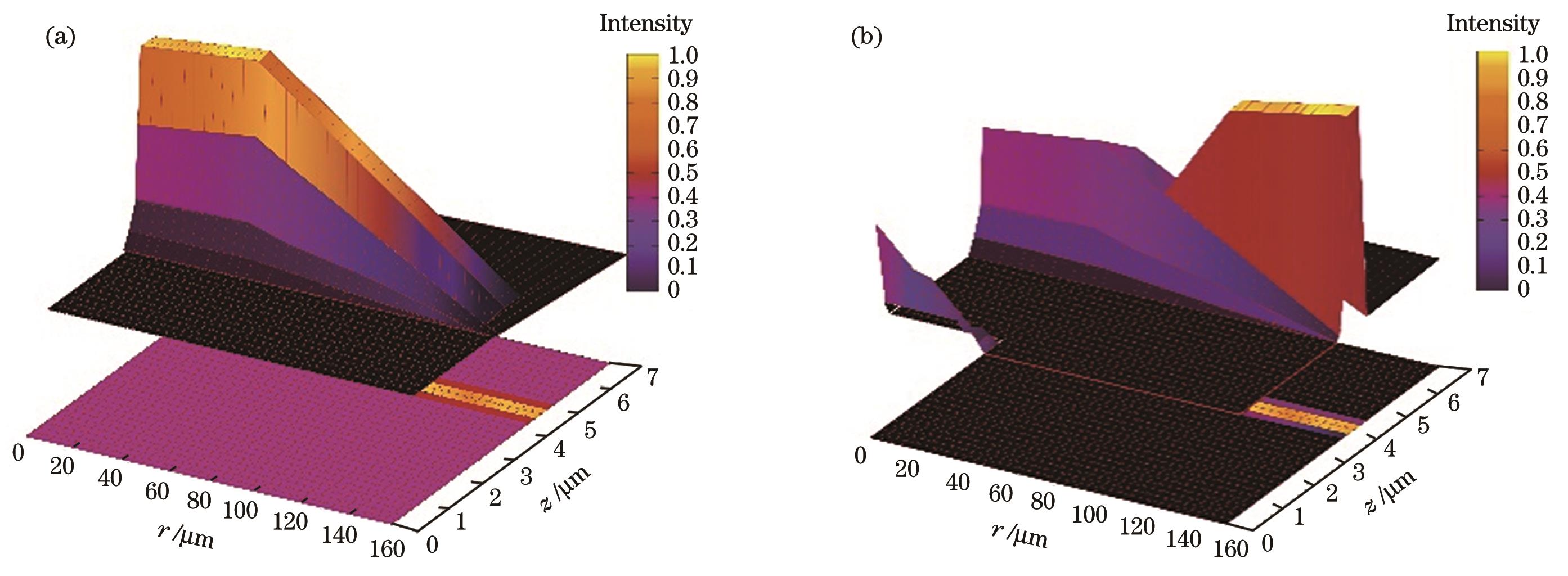
图 1. VCSEL的光场强度分布图。(a)孔径为15 μm;(b)孔径为300 μm
Fig. 1. VCSEL light field intensity distribution. (a) Aperture of 15 μm; (b) aperture of 300 μm
为了解决这一问题,我们设计了多环形腔结构[

图 2. VCSEL结构示意图。(a)传统结构;(b)多环形腔结构
Fig. 2. Schematics of VCSEL structures. (a) Traditional structure; (b) multi-ring cavity structure

图 3. 不同
Fig. 3. Light field distributions of multi-ring cavity VCSELs with different
3 器件制备
采用同一芯片,在同一工艺条件下,制备了光孔外部直径完全相同的传统结构和新型结构的高功率VCSEL器件。对于外延结构,采用金属有机化合物化学气相沉淀(MOCVD)技术在n型GaAs衬底上生长,结构包括41对Si掺杂N型DBR和24对Be掺杂P型 DBR,有源区包含3个GaAs/AlGaAs量子阱结构,作为氧化限制层的高Al层Al0.98Ga0.02As位于P型DBR与有源区之间。外延生长之后,进行紫外光刻、电感耦合等离子体(ICP)刻蚀、湿法氧化、生长SiO2掩模、溅射电极、金属剥离、减薄封装等,具体流程如
与传统结构相比,多环形腔结构VCSEL在制备过程中的有些关键技术值得关注,例如:对于图形复杂的多环结构,需要图形对准且相嵌,因此精确的套刻对准为制备良好器件奠定了基础;对于ICP刻蚀工艺,需要研究刻蚀工艺参数对台面侧壁陡直度的影响,这有助于制备均匀的氧化限制层;对于湿法氧化工艺,在进行多环氧化时需要对氧化温度进行优化调整,研究温度对氧化速率及氧化孔形状的作用规律,从而精确控制氧化孔的尺寸和形状。
4 结果与讨论

图 5. 不同
Fig. 5. Near-field test results of multi-ring cavity VCSELs with different

图 6. 新型结构VCSEL的远场分布图和光谱图。(a)远场分布图;(b)光谱图
Fig. 6. Far-field distribution and spectrum of novel structure VCSEL. (a) Far-field distribution; (b) spectrum
在室温下利用半导体综合参数测试仪对上述几种结构VCSEL的连续工作状态进行测试,得到的功率-电流(P-I)特性曲线如
可以看出,当注入电流达到阈值电流后,输出功率随电流的增大而增加,当电流增大到一定时,输出功率达到最大,随着电流的进一步增大,输出功率下降。这是由于随着电流的注入,器件内部产生大量热,器件温度升高,尤其是有源区的温升较大,故器件内的各种非辐射复合得到增强,内、外量子效率降低,更多注入的电功率转化为热功率,进而输出功率降低。另外,传统结构VCSEL[
5 结论
通过分析大孔径VCSEL载流子分布不均匀的原因,设计了多环形腔结构VCSEL并对新型结构的光场进行了仿真,结果显示,通过优化环形腔的尺寸和出光区域占比,可以优化光场分布。在此基础上,在同一外延片上同时制备了出光孔外部直径完全相同的传统结构和新型结构VCSEL,对其光场均匀性及输出特性等进行了比较分析。结果表明:新型结构改善了传统结构载流子聚集效应造成的光场分布不均现象,其中占空比为67%的新型多环形腔结构VCSEL的近场分布最佳,且阈值电流有所降低;当注入电流为0.8 A时,室温下连续输出功率最高达到140 mW,较传统结构提高了近56%,远场呈现高斯分布,光束质量较好。研究结果满足了光通信领域VCSEL对高功率高光束质量半导体激光源的需求,进一步拓展了VCSEL在智能设备领域的应用范围。
[1] Soda H, Iga K I, Kitahara C, et al. GaInAsP/InP surface emitting injection lasers[J]. Japanese Journal of Applied Physics, 1979, 18(12): 2329-2330.
[2] 王立军, 宁永强, 秦莉, 等. 大功率半导体激光器研究进展[J]. 发光学报, 2015, 36(1): 1-19.
[3] Zhou D L, Seurin J F, Xu G Y, et al. Progress on high-power high-brightness VCSELs and applications[J]. Proceedings of SPIE, 2015, 9381: 93810B.
[4] Seurin J F, Zhou D L, Xu G Y, et al. High-efficiency VCSEL arrays for illumination and sensing in consumer applications[J]. Proceedings of SPIE, 2016, 9766: 97660D.
[5] Moench H, Carpaij M, Gerlach P, et al. VCSEL-based sensors for distance and velocity[J]. Proceedings of SPIE, 2016, 9766: 97660A.
[6] Inoue S, Nishimura S, Nakahama M, et al. High-speed wavelength switching of tunable MEMS vertical cavity surface emitting laser by ringing suppression[J]. Japanese Journal of Applied Physics, 2018, 57(4): 040308.
[7] Wei M S, Xing F, You Z. A real-time detection and positioning method for small and weak targets using a 1D morphology-based approach in 2D images[J]. Light: Science & Applications, 2018, 7(5): 18006.
[8] Iga K. Forty years of vertical-cavity surface-emitting laser: invention and innovation[J]. Japanese Journal of Applied Physics, 2018, 57(8S2): 08.
[9] Ebeling K J, Michalzik R, Moench H. Vertical-cavity surface-emitting laser technology applications with focus on sensors and three-dimensional imaging[J]. Japanese Journal of Applied Physics, 2018, 57(8S2): 08.
[10] Kuramoto M, Kobayashi S, Akagi T, et al. Watt-class blue vertical-cavity surface-emitting laser arrays[J]. Applied Physics Express, 2019, 12(9): 091004.
[11] Li M J, Li K M, Chen X, et al. Single-mode VCSEL transmission for short reach communications[J]. Journal of Lightwave Technology, 2021, 39(4): 868-880.
[12] 李建军, 褚春艳, 卢玮彤, 等. 微透镜阵列的制备与应用研究进展[J]. 光学学报, 2021, 41(21): 2100001.
[13] Guo X, Shi L, Li C, et al. Research of the use of silver nanowires as a current spreading layer on vertical-cavity surface-emitting lasers[J]. Chinese Physics B, 2016, 25(11): 114208.
[14] Hassan A M A, Gu X D, Nakahama M, et al. High-power operations of single-mode surface grating long oxide aperture VCSELs[J]. Applied Physics Letters, 2021, 119(19): 191103.
[15] Hassan A M A, Gu X D, Nakahama M, et al. High power surface grating slow-light VCSEL[J]. Applied Physics Express, 2021, 14(9): 092006.
[16] Hu S T, Hassan A M A, Gu X D, et al. Surface grating loaded VCSEL with single mode power of over 80 mW[J]. IEICE Electronics Express, 2021, 18(11): 20210202.
[17] 潘智鹏, 李伟, 戚宇轩, 等. 光子晶体垂直腔面发射激光器的设计分析[J]. 光学学报, 2022, 42(14): 1414002.
[18] 王翔媛, 崔碧峰, 李彩芳, 等. 垂直腔面发射激光器横模控制方法的研究进展[J]. 激光与光电子学进展, 2021, 58(7): 0700008.
[19] Yoshida M, De Zoysa M, Ishizaki K, et al. Double-lattice photonic-crystal resonators enabling high-brightness semiconductor lasers with symmetric narrow-divergence beams[J]. Nature Materials, 2019, 18(2): 121-128.
[20] Hirose K, Liang Y, Kurosaka Y, et al. Watt-class high-power, high-beam-quality photonic-crystal lasers[J]. Nature Photonics, 2014, 8(5): 406-411.
[21] Khan Z, Shih J C, Chao R L, et al. High-brightness and high-speed vertical-cavity surface-emitting laser arrays[J]. Optica, 2020, 7(4): 267-275.
[22] 郑世奇. 基于速率方程的垂直腔面发射激光器数值模拟与特性研究[D]. 北京: 北京邮电大学, 2006.
ZhengS Q. Numerical simulation and characteristic research of vertical cavity surface emitting laser based on rate equation[D]. Beijing: Beijing University of Posts and Telecommunications, 2006.
[23] 杨浩, 郭霞, 关宝璐, 等. 注入电流对垂直腔面发射激光器横模特性的影响[J]. 物理学报, 2008, 57(5): 2959-2965.
Yang H, Guo X, Guan B L, et al. The influence of injection current on transverse mode characteristics of vertical-cavity surface-emitting lasers[J]. Acta Physica Sinica, 2008, 57(5): 2959-2965.
Article Outline
闫观鑫, 郝永芹. 高光束质量大功率垂直腔面发射激光器[J]. 中国激光, 2024, 51(8): 0801001. Guanxin Yan, Yongqin Hao. High-Beam-Quality High-Power Vertical-Cavity Surface-Emitting Laser[J]. Chinese Journal of Lasers, 2024, 51(8): 0801001.
