银纳米颗粒复合非晶氧化镓光电探测器的制备与研究
Thanks to the low false alarm rate and high signal-to-noise ratio, deep ultraviolet (DUV) photodetector (PD) shows great application potential in ozone hole detection, high-voltage electric fire alarm, stealth bomber, and missile alarm. Gallium oxide (Ga2O3) is one of the most ideal materials for DUV PDs due to its suitable and tunable bandgap (4.5-5.3 eV), simple preparation process, and high stability. Nowadays, many studies focused on crystalline Ga2O3 film DUV PDs, but the lattice mismatch and strict growth parameters during the preparation put forward higher requirements for substrate materials and growth equipment. Compared with crystalline Ga2O3, amorphous Ga2O3 films have low preparation requirements and are easier to generate larger photocurrents due to the promotion of carrier separation by intrinsic defects. However, amorphous Ga2O3 is prone to higher dark current due to more defects. It is necessary to introduce noble metal Ag nanoparticles (Ag-NPs) to improve the photodetection performance of amorphous Ga2O3. On one hand, the formation of Schottky barriers between Ag-NPs and Ga2O3 films helps reduce the dark current of amorphous Ga2O3. On the other hand, the surface plasmon vibration of Ag-NPs can enhance the absorption of Ga2O3to UV light. Additionally, Ag-NPs can generate a large number of hot carriers under UV light to allow hot electrons with sufficient energy to overcome the Schottky barriers. We provide a feasible approach to realize DUV PDs with low dark current and high photo-to-dark current ratio (PDCR).
Amorphous Ga2O3 films are grown on sapphire substrates by the facile radio frequency (RF) magnetron sputtering technology. The sputtering is carried out at room temperature for 70 min with chamber pressure and Argon flow rate of 1 Pa and 20 sccm respectively. The obtained Ga2O3 films are cut into four parts, and three of them are continuously sputtered with Ag-NPs on the Ga2O3surface by direct-current (DC) magnetron sputtering. The sputtering time is 5, 10, and 20 s respectively. The obtained samples are labeled as 5 s Ag-NPs/Ga2O3, 10 s Ag-NPs/Ga2O3, and 20 s Ag-NPs/Ga2O3. Finally, the four samples obtained previously are annealed in a tube furnace for 2 h at an annealing temperature of 200 °C. The crystal structure of the sample is characterized by X-ray diffractometer (XRD), the cross-section morphology of the sample is by scanning electron microscope (SEM), and the surface morphology of the sample is by atomic force microscope (AFM). Additionally, the absorption spectrum features Q6 ultraviolet-visible (UV-Vis) spectrophotometer, and the low-pressure mercury lamps with wavelengths of 254 nm and 365 nm are employed as the ultraviolet light source. A pair of cylindrical metal indium (In) with a diameter of 1 mm and a spacing of 1 mm is pressed on the surface of samples as electrodes, and the current-voltage (I-V) characteristics and transient response curve (I-t) of the PDs are measured by a B1505A power device analyzer.
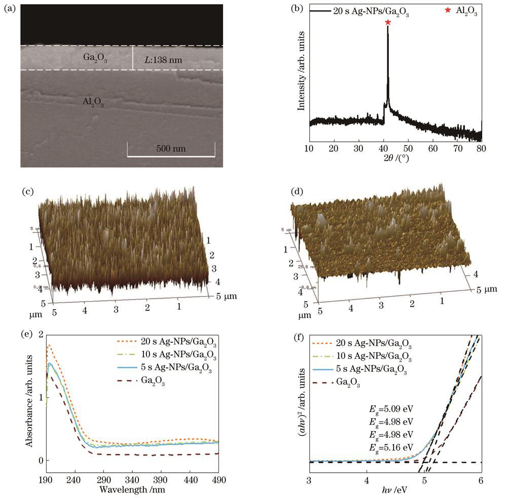
AFM results confirm the introduction of Ag-NPs on the surface of amorphous Ga2O3 films, and the surface mean square root (RMS) roughness of the Ag-NPs/Ga2O3 film after sputtering Ag nanoparticles for 20 s is significantly increased from 0.218 to 6.390 nm [Figs. 1 (c) and 1(d)]. Meanwhile, the absorption of Ga2O3 to UV light also increases obviously after sputtering Ag-NPs [Fig. 1 (e)]. 20 s Ag-NPs/Ga2O3 presents a lower dark current than amorphous Ga2O3 due to the Schottky junction formed between Ag-NPs and Ga2O3 films, which further forms a potential barrier and reduces the dark current [Fig. 2 (a)]. Under the irradiation of 254 nm UV light, Ag-NPs/Ga2O3 films exhibit a higher photocurrent than amorphous Ga2O3. In particular, the photocurrent of 20 s Ag-NPs/Ga2O3 at 5 V is 18.8 times higher than that of amorphous Ga2O3[Fig. 2 (b)]. This may be due to the enhanced scattering of UV light by the plasmonic vibrations of the Ag-NPs on the surface of Ga2O3 films, thus leading to enhanced absorption of UV light by Ga2O3 and an increase in the photocurrent of the Ag-NPs/Ga2O3 PD. Additionally, the Ag-NPs vibration may generate a large number of hot carriers to have enough energy to cross the Schottky barriers between Ag-NPs and Ga2O3 films, which leads to an increase in the photocurrent of the PD. At this point, the PDCR is as high as 5.9×10⁵, the rejection ratio (254 nm/365 nm) is 1.6×10⁴[Fig. 2 (c)], and the responsivity is 36.1 mA/W [Fig. 3 (c)], with the detectivity of 2×10¹⁴ Jones and external quantum efficiency of 17.7% [Fig. 3 (d)]. Meanwhile, both the amorphous Ga2O3 detector and the Ag-NPs/Ga2O3 detector have short response time (Fig. 4).
In summary, the Ag-NP composite amorphous Ga2O3 film DUV PD is prepared by a room temperature magnetron sputtering technology. The PD exhibits an excellent photodetection performance. Under 5 V voltage, the dark current of the detector is as low as 94 fA and the PDCR is as high as 5.9×10⁵, and the rejection ratio (254 nm/365 nm) is 1.6×10⁴, with the responsivity of 36.1 mA/W, detectivity of 2×10¹⁴ Jones, and external quantum efficiency of 17.7%. This is not only attributed to the plasmonic vibration of Ag-NPs under UV light, which scatters more incident light into the Ga2O3 film layer to enhance the UV light absorption of the Ga2O3 films, but also to the generation of a large number of hot carriers by Ag-NPs under UV light. These hot carriers enable the hot electrons to overcome the Schottky barriers formed by Ag-NPs and Ga2O3 films, which brings about a significant increase in the PD photocurrent. In addition, the formation of the Schottky barriers between Ag-NPs and Ga2O3 films helps reduce the dark current in the amorphous Ga2O3. This study implies that the introduction of noble metal nanoparticles provides a viable solution to DUV PDs with low cost, dark current, and high PDCR.
许强, 杨莉莉, 刘增, 张茂林, 李山, 唐为华. 银纳米颗粒复合非晶氧化镓光电探测器的制备与研究[J]. 光学学报, 2023, 43(20): 2004003. Qiang Xu, Lili Yang, Zeng Liu, Maolin Zhang, Shan Li, Weihua Tang. Preparation and Study of Ag Nanoparticles Composite Amorphous Gallium Oxide Photodetector[J]. Acta Optica Sinica, 2023, 43(20): 2004003.


