银纳米颗粒复合非晶氧化镓光电探测器的制备与研究
Thanks to the low false alarm rate and high signal-to-noise ratio, deep ultraviolet (DUV) photodetector (PD) shows great application potential in ozone hole detection, high-voltage electric fire alarm, stealth bomber, and missile alarm. Gallium oxide (Ga2O3) is one of the most ideal materials for DUV PDs due to its suitable and tunable bandgap (4.5-5.3 eV), simple preparation process, and high stability. Nowadays, many studies focused on crystalline Ga2O3 film DUV PDs, but the lattice mismatch and strict growth parameters during the preparation put forward higher requirements for substrate materials and growth equipment. Compared with crystalline Ga2O3, amorphous Ga2O3 films have low preparation requirements and are easier to generate larger photocurrents due to the promotion of carrier separation by intrinsic defects. However, amorphous Ga2O3 is prone to higher dark current due to more defects. It is necessary to introduce noble metal Ag nanoparticles (Ag-NPs) to improve the photodetection performance of amorphous Ga2O3. On one hand, the formation of Schottky barriers between Ag-NPs and Ga2O3 films helps reduce the dark current of amorphous Ga2O3. On the other hand, the surface plasmon vibration of Ag-NPs can enhance the absorption of Ga2O3to UV light. Additionally, Ag-NPs can generate a large number of hot carriers under UV light to allow hot electrons with sufficient energy to overcome the Schottky barriers. We provide a feasible approach to realize DUV PDs with low dark current and high photo-to-dark current ratio (PDCR).
Amorphous Ga2O3 films are grown on sapphire substrates by the facile radio frequency (RF) magnetron sputtering technology. The sputtering is carried out at room temperature for 70 min with chamber pressure and Argon flow rate of 1 Pa and 20 sccm respectively. The obtained Ga2O3 films are cut into four parts, and three of them are continuously sputtered with Ag-NPs on the Ga2O3surface by direct-current (DC) magnetron sputtering. The sputtering time is 5, 10, and 20 s respectively. The obtained samples are labeled as 5 s Ag-NPs/Ga2O3, 10 s Ag-NPs/Ga2O3, and 20 s Ag-NPs/Ga2O3. Finally, the four samples obtained previously are annealed in a tube furnace for 2 h at an annealing temperature of 200 °C. The crystal structure of the sample is characterized by X-ray diffractometer (XRD), the cross-section morphology of the sample is by scanning electron microscope (SEM), and the surface morphology of the sample is by atomic force microscope (AFM). Additionally, the absorption spectrum features Q6 ultraviolet-visible (UV-Vis) spectrophotometer, and the low-pressure mercury lamps with wavelengths of 254 nm and 365 nm are employed as the ultraviolet light source. A pair of cylindrical metal indium (In) with a diameter of 1 mm and a spacing of 1 mm is pressed on the surface of samples as electrodes, and the current-voltage (I-V) characteristics and transient response curve (I-t) of the PDs are measured by a B1505A power device analyzer.
AFM results confirm the introduction of Ag-NPs on the surface of amorphous Ga2O3 films, and the surface mean square root (RMS) roughness of the Ag-NPs/Ga2O3 film after sputtering Ag nanoparticles for 20 s is significantly increased from 0.218 to 6.390 nm [Figs. 1 (c) and 1(d)]. Meanwhile, the absorption of Ga2O3 to UV light also increases obviously after sputtering Ag-NPs [Fig. 1 (e)]. 20 s Ag-NPs/Ga2O3 presents a lower dark current than amorphous Ga2O3 due to the Schottky junction formed between Ag-NPs and Ga2O3 films, which further forms a potential barrier and reduces the dark current [Fig. 2 (a)]. Under the irradiation of 254 nm UV light, Ag-NPs/Ga2O3 films exhibit a higher photocurrent than amorphous Ga2O3. In particular, the photocurrent of 20 s Ag-NPs/Ga2O3 at 5 V is 18.8 times higher than that of amorphous Ga2O3[Fig. 2 (b)]. This may be due to the enhanced scattering of UV light by the plasmonic vibrations of the Ag-NPs on the surface of Ga2O3 films, thus leading to enhanced absorption of UV light by Ga2O3 and an increase in the photocurrent of the Ag-NPs/Ga2O3 PD. Additionally, the Ag-NPs vibration may generate a large number of hot carriers to have enough energy to cross the Schottky barriers between Ag-NPs and Ga2O3 films, which leads to an increase in the photocurrent of the PD. At this point, the PDCR is as high as 5.9×10⁵, the rejection ratio (254 nm/365 nm) is 1.6×10⁴[Fig. 2 (c)], and the responsivity is 36.1 mA/W [Fig. 3 (c)], with the detectivity of 2×10¹⁴ Jones and external quantum efficiency of 17.7% [Fig. 3 (d)]. Meanwhile, both the amorphous Ga2O3 detector and the Ag-NPs/Ga2O3 detector have short response time (Fig. 4).
In summary, the Ag-NP composite amorphous Ga2O3 film DUV PD is prepared by a room temperature magnetron sputtering technology. The PD exhibits an excellent photodetection performance. Under 5 V voltage, the dark current of the detector is as low as 94 fA and the PDCR is as high as 5.9×10⁵, and the rejection ratio (254 nm/365 nm) is 1.6×10⁴, with the responsivity of 36.1 mA/W, detectivity of 2×10¹⁴ Jones, and external quantum efficiency of 17.7%. This is not only attributed to the plasmonic vibration of Ag-NPs under UV light, which scatters more incident light into the Ga2O3 film layer to enhance the UV light absorption of the Ga2O3 films, but also to the generation of a large number of hot carriers by Ag-NPs under UV light. These hot carriers enable the hot electrons to overcome the Schottky barriers formed by Ag-NPs and Ga2O3 films, which brings about a significant increase in the PD photocurrent. In addition, the formation of the Schottky barriers between Ag-NPs and Ga2O3 films helps reduce the dark current in the amorphous Ga2O3. This study implies that the introduction of noble metal nanoparticles provides a viable solution to DUV PDs with low cost, dark current, and high PDCR.
1 引 言
大气层中的臭氧层等对波长低于280 nm的深紫外(DUV)光具有强烈的吸收和散射作用,使得进入到地球大气层内的太阳辐射中深紫外光几乎为零。干净的背景噪声赋予了深紫外光电探测较低的误警率和较高的信噪比等优点,使得其受到越来越多的学者的关注,并在臭氧空洞探测、高压电火灾报警、隐形轰炸机和导弹报警方面具有很大的应用潜力[1-2]。深紫外光电探器主要采用宽禁带半导体材料,常见的包括AlGaN[3-4]、MgZnO[5-6]、金刚石[7]、氧化镓(Ga2O3)[8]等。其中,Ga2O3作为一种新型的光电材料,无须进行合金化过程,制备简单、稳定性高,且Ga2O3具有适合深紫外波段探测的可调的能带带隙(4.5~5.3 eV),是制备深紫外光电探测器最理想的材料之一[9]。Ga2O3共有五种同分异构体,分别为α-Ga2O3、β-Ga2O3、ε-Ga2O3、δ-Ga2O3和γ-Ga2O3,其中最稳定的为β相Ga2O3[10]。目前很多研究都集中在结晶相的Ga2O3薄膜上,但是高质量的晶体薄膜在制备过程中容易受到衬底的晶格匹配和严格的生长参数的影响,从而对衬底材料和薄膜生长设备均提出了较高的要求,因此Ga2O3晶体薄膜往往具有制备成本高、重现性差等缺点。
非晶Ga2O3薄膜一般采用磁控溅射、脉冲激光沉积等技术,制备过程简单、成本低廉[11]。相较于结晶Ga2O3,非晶Ga2O3含有更高密度的氧空位等缺陷,这些缺陷一方面有助于捕获光生载流子,促进电荷分离;另一方面又可以作为光生载流子的复合中心,降低电荷分离效率[12],因此非晶Ga2O3更容易在深紫外光的激发下展现出大的光电流。综上这些优点使得非晶Ga2O3薄膜在紫外光电器件材料中受到关注。但非晶Ga2O3薄膜由于其较差的结晶性,往往器件的暗电流也较高。贵金属纳米颗粒如Au、Ag、Cu等[13]具有固有的等离子振动频率,紫外光下的贵金属表面等离子振动可以增强对入射光的散射作用,从而有利于提高探测器对入射光的吸收和探测[14]。且紫外光照下贵金属纳米颗粒会产生大量的热载流子,使得热电子有足够的能量克服Ag纳米颗粒与Ga2O3薄膜间的肖特基势垒,从而增加探测器的光电流。此外,具有合适功函数的金属的引入还有助于在半导体-金属界面形成势垒区,使得暗电流进一步降低。因此,为了进一步提高非晶Ga2O3基光电探测器对深紫外信号的探测灵敏度,向非晶Ga2O3薄膜表面引入贵金属纳米颗粒是一种可行的实现方式。目前已有许多报道通过引入贵金属颗粒来提高探测器的性能。如石雄林等[15]利用快速热退火的方法在β-Ga2O3薄膜表面形成了直径为12~40 nm的铝纳米颗粒(Al-NPs),并成功制备了Al-NPs/β-Ga2O3日盲紫外探测器。Al纳米颗粒的存在不仅降低了探测器件的暗电流,同时也增大了探测器件的光响应度和探测率。除此之外,铝纳米颗粒增加了β-Ga2O3薄膜对入射光的散射,且铝纳米颗粒周围电磁场的增强促使了器件的内部增益变大,从而使器件光响应度和探测率增大。10 V偏压下,Al-NPs/β-Ga2O3探测器的光响应度达到了2.7 A/W,探测率达到了1.35×1014 cm·Hz1/2·W-1,另外,Al-NPs/β-Ga2O3探测器的衰减率(103)得到大幅提高。An等[16]通过在β-Ga2O3薄膜上沉积Au纳米颗粒(Au-NPs)制备复合薄膜,然后进行后热处理。与β-Ga2O3薄膜相比,在Au-NPs/β-Ga2O3的紫外-可见光谱中观察到510 nm附近有显著的吸收。结果表明,Au-NPs/β-Ga2O3的光响应在254 nm+532 nm光照射下的光电探测器远高于在254 nm光照射下的光电探测器,同时由表面等离子激元效应辅助的β-Ga2O3薄膜光电探测器具有高鲁棒性和良好的可重复性,能够表现出相对较快的响应速度和恢复速度,表明在Ga2O3表面引入金属纳米颗粒可有效改善光电探测器的性能。
银(Ag)作为一种贵金属材料,其固有的等离子振动吸收峰位于400 nm附近,且Ag纳米颗粒具有合适的功函数(4.6 eV)[17],能够与非晶Ga2O3薄膜形成肖特基接触界面。因此,本文旨在利用金属Ag纳米颗粒复合Ga2O3薄膜(Ag-NPs/Ga2O3)来提高探测器的光电流并降低其暗电流。具体操作是采用常温射频磁控溅射技术在蓝宝石衬底表面溅射一层Ga2O3薄膜,再通过直流磁控溅射技术将Ag纳米颗粒溅射到Ga2O3薄膜表面形成复合薄膜。基于Ag-NPs/Ga2O3得到的光电探测器表现出优异的深紫外探测性能,在5 V偏压下,探测器的暗电流低至94 fA,光暗电流比高达5.9×105,254 nm/365 nm波长抑制比达到1.6×10⁴,其响应度为36.1 mA/W,探测率为2×1014 Jones(探测率单位),外量子效率为17.7%,较相应的Ga2O3基光电探测器均得到了较大的提升。
2 实验方法
本文采用射频磁控溅射技术在(0001)面的蓝宝石衬底上生长Ga2O3薄膜。溅射在常温下进行,溅射时的腔室气压和所通的氩气流量分别为1 Pa和20 sccm,溅射总时间为70 min。溅射完毕后将所得到的Ga2O3薄膜切成4份,取其中3份采用直流磁控溅射技术继续在Ga2O3表面溅射Ag纳米颗粒,溅射时间分别为5、10、20 s,获得的样品分别标记为5 s Ag-NPs/Ga2O3、10 s Ag-NPs/Ga2O3、20 s Ag-NPs/Ga2O3[18]。最后,将上述得到的4份样品放入管式炉中退火2 h,退火温度为200 ℃。用X射线衍射仪(XRD)对样品的晶体结构进行表征,用扫描电子显微镜(SEM)对所得样品断面形貌进行表征,用原子力显微镜(AFM)对所得样品表面形貌进行表征,用上海元析Q6紫外-可见(UV-Vis)分光光度计对样品的光谱吸收进行表征,采用波长分别为254 nm和365 nm的低压汞灯作为紫外光光源。在样品表面压上直径为1 mm、间距为1 mm的圆柱形金属铟作为电极,并使用B1505A功率器件分析仪测量Ag-NPs/Ga2O3薄膜光电探测器的电流-电压(I-V)特性和瞬态响应(I-t)特性[19-20]。
3 分析与讨论
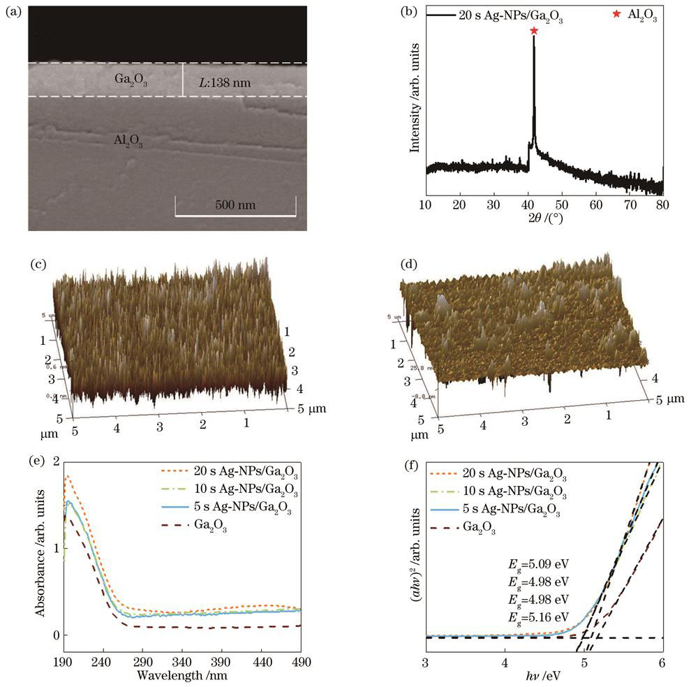
图 1. Ga2O3薄膜材料表征。(a)蓝宝石衬底上常温生长的Ga2O3薄膜断面SEM图像;(b)20 s Ag-NPs/Ga2O3的XRD图;(c)Ga2O3的AFM图像;(d)20 s Ag-NPs/Ga2O3的AFM图像;(e)Ga2O3和Ag-NPs/Ga2O3的吸收光谱图;(f)(αhν)2-hν曲线图
Fig. 1. Material characterization of Ga2O3 film. (a) SEM image of cross section of Ga2O3 film grown on sapphire substrate at room temperature; (b) XRD image of 20 s Ag-NPs/Ga2O3; (c) AFM image of Ga2O3; (d) AFM image of 20 s Ag-NPs/Ga2O3; (e) absorption spectra of Ga2O3 and Ag-NPs/Ga2O3; (f) curve of (αhν)2-hν
表 1. 薄膜光电探测器的上升沿和下降沿时间常数
Table 1. Time constants of rising and falling edges of thin film photodetectors
|
表 2. 20 s Ag-NPs/Ga2O3薄膜光电探测器与其他最近报道的Ga2O3基光电探测器的性能对比
Table 2. Performance comparison of 20 s Ag-NPs/Ga2O3 thin film photodetector with other recently reported Ga2O3-based photodetectors
|
式中:α为吸收系数;hν为入射光子能;A2表示吸收边的斜率;Eg为光学带隙。从图中可以看出,其Ga2O3、5 s Ag-NPs/Ga2O3、10 s Ag-NPs/Ga2O3、20 s Ag-NPs/Ga2O3的光学带隙分别为5.16、4.98、4.98、5.09 eV左右,与所报道的Ga2O3相近[22],这为制备高性能的光电探测器提供了保证。此外,Ag-NPs/Ga2O3薄膜较非晶Ga2O3薄膜表现出更低的光学带隙,这是由于Ag纳米颗粒增强了Ga2O3薄膜对紫外光的吸收,使得Ag-NPs/Ga2O3薄膜的吸光度高于非晶Ga2O3薄膜,且吸收带边略有红移,根据Tauc关系式,Ag-NPs/Ga2O3薄膜的光学带隙低于非晶Ga2O3薄膜。
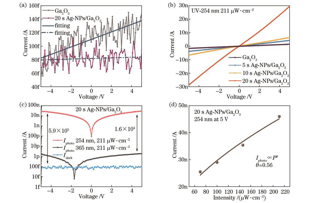
图 2. Ga2O3光电探测器的I-V特性曲线图。(a)在黑暗下非晶Ga2O3和Ag-NPs/Ga2O3薄膜光电探测器的I-V特性曲线;(b)在254 nm紫外光照射下非晶Ga2O3和Ag-NPs/Ga2O3薄膜光电探测器的I-V特性曲线;(c)20 s Ag-NPs/Ga2O3薄膜光电探测器分别在无光照、254 nm和365 nm光照下的I-V特性曲线;(d)光电流随光强变化的曲线拟合
Fig. 2. I-V curves of Ga2O3 photodetectors. (a) I-V curves of amorphous Ga2O3 and Ag-NPs/Ga2O3 thin film photodetectors in dark; (b) I-V curves of amorphous Ga2O3 and Ag-NPs/Ga2O3 thin film photodetectors irradiated by 254 nm ultraviolet (UV) light; (c) I-V curves of 20 s Ag-NPs/Ga2O3thin film photodetector under dark, 254 nm, and 365 nm UV lights, respectively; (d) fitted relation curve of photocurrent with light intensity
通过拟合,θ(拟合幂数)值为0.56。
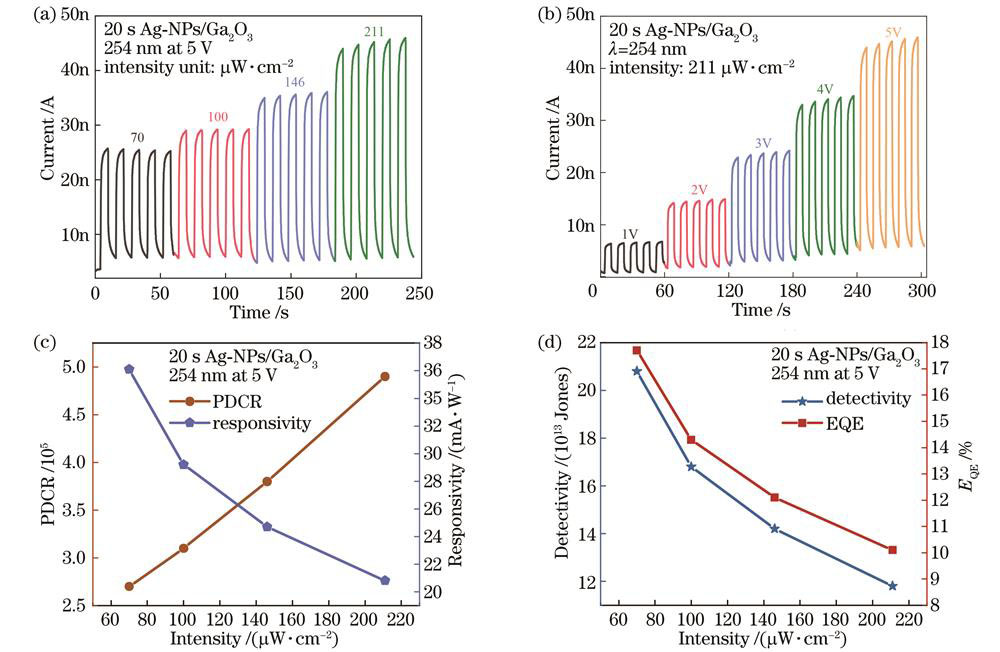
图 3. Ga2O3光电探测器的性能测试。(a)20 s Ag-NPs/Ga2O3薄膜光电探测器在254 nm紫外光照射下5 V偏压时不同光强的I-t曲线;(b)20 s Ag-NPs/Ga2O3薄膜光电探测器在254 nm紫外光照射下光强为211 μW/cm2时不同偏压下的I-t曲线;(c)PDCR和光响应度与光强的线性关系曲线;(d)探测率和外量子效率与光强的线性关系曲线
Fig. 3. Performance test of Ga2O3 photodetectors. (a) I-t curve of 20 s Ag-NPs/Ga2O3 thin film photodetector under 254 nm UV irradiation at 5 V bias with different light intensities; (b) I-t curve of 20 s Ag-NPs/Ga2O3 thin film photodetector irradiated by 254 nm UV light with intensity of 211 μW/cm2under different bias voltages; (c) linear relationship curve of PDCR and responsivity with light intensity; (d) linear relationship curve of detectivity and EQE with light intensity
本文进一步研究了在不同光强下的Ag-NPs/Ga2O3薄膜探测器的性能,如
式中:Iphoto、Idark分别为光、暗电流;Plight为入射光光强;S为有效照明面积。当入射光光强为70 μW/cm2、偏压为5 V时,20 s Ag-NPs/Ga2O3薄膜光电探测器的光响应度R为36.1 mA/W。但是该探测器的光响应度反而随光强的增加从36.1 mA/W下降到20.8 mA/W,这种现象也常见于许多其他的探测器中,这是由于探测器会在高光强下发生自热效应。随着光强的增加,虽然会生成更多的光生载流子,但同时由于载流子散射和复合增强,很多光生载流子在被激发到导带前被重新复合,载流子输运效率下降,这就导致探测器的响应度随入射光强增大而减小[27]。探测器的探测率用D*表示,它是衡量探测器噪声性能的重要参数,是噪声等效功率(探测器可探测到的最小光信号的量值)的倒数,其定义式[28]为
式中,q为电子电荷。将
式中:h为普朗克常量;c为光速;λ为入射光波长。将
为了研究光电探测器的瞬态响应表现,本文分别测试了非晶Ga2O3和Ag-NPs/Ga2O3探测器在电压为5 V、波长为254 nm光照和黑暗状态下交替的瞬态反应,如图
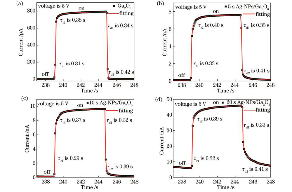
图 4. 不同薄膜光电探测器的上升沿和下降沿的拟合曲线。(a)Ga2O3;(b)5 s Ag-NPs/Ga2O3;(c)10 s Ag-NPs/Ga2O3;(d)20 s Ag-NPs/Ga2O3
Fig. 4. Fitting curves of rising and falling edges of different thin film photodetectors. (a) Ga2O3; (b) 5 s Ag-NPs/Ga2O3; (c) 10 s Ag-NPs/Ga2O3; (d) 20 s Ag-NPs/Ga2O3
式中:I0为稳定态的光电流;A、B为常数;t是打开和关闭的时间;τ1和τ2为弛豫时间常数,
为了更好地比较20 s Ag-NPs/Ga2O3薄膜光电探测器的性能,在
4 结 论
综上所述,在常温生长的非晶Ga2O3薄膜的基础上引入Ag纳米颗粒,成功制备了金属Ag纳米颗粒复合Ga2O3薄膜的日盲紫外光电探测器。该探测器表现出优异的探测性能,在5 V偏压下,探测器的暗电流低至94 fA,光暗电流比高达5.9×105,254 nm/365 nm波长抑制比达到1.6×10⁴,响应度为36.1 mA/W,探测率为2×1014 Jones,外量子效率为17.7%。这不仅得益于紫外光下Ag纳米颗粒的等离子振动使得更多的入射光散射到Ga2O3薄膜层,从而提高了Ga2O3薄膜对光的吸收;而且Ag纳米颗粒在紫外光下可产生大量热载流子,使热电子有足够能量越过Ag纳米颗粒和Ga2O3薄膜形成的肖特基势垒,这两者都极大提高了探测器的光电流。此外,Ag纳米颗粒与Ga2O3薄膜间的肖特基势垒的形成有助于减小非晶Ga2O3的暗电流。本文工作意味着贵金属纳米颗粒的引入为实现低成本、低暗电流、高光暗电流比的日盲紫外探测器提供了一种可行的方案。
[1] 王丹, 王晓丹, 马海, 等. Ga2O3材料的掺杂研究进展[J]. 激光与光电子学进展, 2021, 58(15): 1516025.
[2] Chen X, Liu K W, Zhang Z Z, et al. Self-powered solar-blind photodetector with fast response based on Au/β-Ga2O3 nanowires array film Schottky junction[J]. ACS Applied Materials & Interfaces, 2016, 8(6): 4185-4191.
[3] 吴刚, 唐利斌, 郝群, 等. 基于Pt/GaN/AlGaN异质结高响应度双波段紫外探测器[J]. 光学学报, 2023, 43(3): 0304002.
[4] Varshney U, Aggarwal N, Gupta G. Current advances in solar-blind photodetection technology: using Ga2O3 and AlGaN[J]. Journal of Materials Chemistry C, 2022, 10(5): 1573-1593.
[5] Hou Y N, Mei Z X, Du X L. Semiconductor ultraviolet photodetectors based on ZnO and MgxZn1–xO[J]. Journal of Physics D: Applied Physics, 2014, 47(28): 283001.
[6] Fan M M, Liu K W, Zhang Z Z, et al. High-performance solar-blind ultraviolet photodetector based on mixed-phase ZnMgO thin film[J]. Applied Physics Letters, 2014, 105(1): 011117.
[7] Lu Y J, Lin C N, Shan C X. Optoelectronic diamond: growth, properties, and photodetection applications[J]. Advanced Optical Materials, 2018, 6(20): 1800359.
[8] Huang L, Feng Q, Han G Q, et al. Comparison study of β-Ga2O3 photodetectors grown on sapphire at different oxygen pressures[J]. IEEE Photonics Journal, 2017, 9(4): 1-8.
[9] Ji X Q, Yin X M, Yuan Y Z, et al. Amorphous Ga2O3 Schottky photodiodes with high-responsivity and photo-to-dark current ratio[J]. Journal of Alloys and Compounds, 2023, 933: 167735.
[10] 王尘, 张宇超, 范伟航, 等. 氧气退火温度对室温脉冲激光沉积氧化镓薄膜特性的影响[J]. 光学学报, 2022, 42(8): 0831001.
[11] Zhou C Q, Liu K W, Chen X, et al. Performance improvement of amorphous Ga2O3 ultraviolet photodetector by annealing under oxygen atmosphere[J]. Journal of Alloys and Compounds, 2020, 840: 155585.
[12] Heinemann M D, Berry J, Teeter G, et al. Oxygen deficiency and Sn doping of amorphous Ga2O3[J]. Applied Physics Letters, 2016, 108(2): 022107.
[13] 况丹, 徐爽, 史大为, 等. 基于铝纳米颗粒修饰的非晶氧化镓薄膜日盲紫外探测器[J]. 物理学报, 2023, 72(3): 038501.
Kuang D, Xu S A, Shi D W, et al. High performance amorphous Ga2O3 thin film solar blind ultraviolet photodetectors decorated with Al nanoparticles[J]. Acta Physica Sinica, 2023, 72(3): 038501.
[14] Zhao Z Q, Chu C S, Zhang G, et al. Tuning the plasmonic resonance peak for Al nanorods on AlGaN layer to deep ultraviolet band[J]. IEEE Photonics Journal, 2021, 13(5): 4800107.
[15] 石雄林, 刘宏宇, 候爽, 等. 表面等离子体在氧化镓基紫外探测器中的应用[J]. 光电工程, 2018, 45(2): 85-92.
Shi X L, Liu H Y, Hou S, et al. The applications of surface plasmons in Ga2O3 ultraviolet photodetector[J]. Opto-Electronic Engineering, 2018, 45(2): 85-92.
[16] An Y H, Chu X L, Huang Y Q, et al. Au plasmon enhanced high performance β-Ga2O3 solar-blind photo-detector[J]. Progress in Natural Science: Materials International, 2016, 26(1): 65-68.
[17] Wang S L, Wu C, Wu F M, et al. Flexible, transparent and self-powered deep ultraviolet photodetector based on Ag NWs/amorphous gallium oxide Schottky junction for wearable devices[J]. Sensors and Actuators A: Physical, 2021, 330: 112870.
[18] Asanithi P, Chaiyakun S, Limsuwan P. Growth of silver nanoparticles by DC magnetron sputtering[J]. Journal of Nanomaterials, 2012, 2012: 1-8.
[19] Cui S J, Mei Z X, Zhang Y H, et al. Room-temperature fabricated amorphous Ga2O3 high-response-speed solar-blind photodetector on rigid and flexible substrates[J]. Advanced Optical Materials, 2017, 5(19): 1700454.
[20] Xu Y, An Z Y, Zhang L X, et al. Solar blind deep ultraviolet β-Ga2O3 photodetectors grown on sapphire by the Mist-CVD method[J]. Optical Materials Express, 2018, 8(9): 2941-2947.
[21] Qin Y, Long S B, He Q M, et al. Amorphous gallium oxide-based gate-tunable high-performance thin film phototransistor for solar-blind imaging[J]. Advanced Electronic Materials, 2019, 5(7): 1900389.
[22] Han S, Huang X L, Fang M Z, et al. High-performance UV detectors based on room-temperature deposited amorphous Ga2O3 thin films by RF magnetron sputtering[J]. Journal of Materials Chemistry C, 2019, 7(38): 11834-11844.
[23] Liu Z, Zhi Y S, Li S, et al. Comparison of optoelectrical characteristics between Schottky and Ohmic contacts to β-Ga2O3 thin film[J]. Journal of Physics D: Applied Physics, 2020, 53(8): 085105.
[24] Dong L P, Pang T Q, Yu J G, et al. Performance-enhanced solar-blind photodetector based on a CH3NH3PbI3/β-Ga2O3 hybrid structure[J]. Journal of Materials Chemistry C, 2019, 7(45): 14205-14211.
[25] Peng Y K, Zhang Y, Chen Z W, et al. Arrays of solar-blind ultraviolet photodetector based on β-Ga2O3 epitaxial thin films[J]. IEEE Photonics Technology Letters, 2018, 30(11): 993-996.
[26] Wang Y H, Cui W J, Yu J, et al. One-step growth of amorphous/crystalline Ga2O3 phase junctions for high-performance solar-blind photodetection[J]. ACS Applied Materials & Interfaces, 2019, 11(49): 45922-45929.
[27] Li S, Yue J Y, Wu C, et al. Self-powered ultraviolet photodetector based on β-Ga2O3/WO3 NPs heterojunction with low noise and high visible rejection[J]. IEEE Sensors Journal, 2021, 21(23): 26724-26730.
[28] Zhang Y F, Chen X H, Xu Y, et al. Transition of photoconductive and photovoltaic operation modes in amorphous Ga2O3-based solar-blind detectors tuned by oxygen vacancies[J]. Chinese Physics B, 2019, 28(2): 028501.
[29] Wang Y H, Li H R, Cao J, et al. Ultrahigh gain solar blind avalanche photodetector using an amorphous Ga2O3-based heterojunction[J]. ACS Nano, 2021, 15(10): 16654-16663.
[30] Kumar N, Arora K, Kumar M. High performance, flexible and room temperature grown amorphous Ga2O3 solar-blind photodetector with amorphous indium-zinc-oxide transparent conducting electrodes[J]. Journal of Physics D: Applied Physics, 2019, 52(33): 335103.
[31] Yu J G, Li Q A, Yao H Z, et al. The performance of Al plasmon enhanced β-Ga2O3 solar-blind photodetector[J]. Scientia Sinica Physica, Mechanica & Astronomica, 2022, 52(9): 297305.
[32] Cui S J, Mei Z X, Hou Y N, et al. Enhanced photoresponse performance in Ga/Ga2O3 nanocomposite solar-blind ultraviolet photodetectors[J]. Chinese Physics B, 2018, 27(6): 067301.
[33] Guo D Y, Zhao X L, Zhi Y S, et al. Epitaxial growth and solar-blind photoelectric properties of corundum-structured α‑Ga2O3 thin films[J]. Materials Letters, 2016, 164: 364-367.
[34] Zhu W H, Xiong L X, Si J W, et al. Influence of deposition temperature on amorphous Ga2O3 solar-blind ultraviolet photodetector[J]. Semiconductor Science and Technology, 2020, 35(5): 055037.
[35] Li S, Zhi Y S, Lu C, et al. Broadband ultraviolet self-powered photodetector constructed on exfoliated β-Ga2O3/CuI core-shell microwire heterojunction with superior reliability[J]. The Journal of Physical Chemistry Letters, 2021, 12(1): 447-453.
[36] Wang H B, Chen H Y, Li L, et al. High responsivity and high rejection ratio of self-powered solar-blind ultraviolet photodetector based on PEDOT: PSS/β‑Ga2O3 organic/inorganic p-n junction[J]. The Journal of Physical Chemistry Letters, 2019, 10(21): 6850-6856.
[37] Vieira D H, Badiei N, Evans J E, et al. Improvement of the deep UV sensor performance of a β‑Ga2O3 photodiode by coupling of two planar diodes[J]. IEEE Transactions on Electron Devices, 2020, 67(11): 4947-4952.
许强, 杨莉莉, 刘增, 张茂林, 李山, 唐为华. 银纳米颗粒复合非晶氧化镓光电探测器的制备与研究[J]. 光学学报, 2023, 43(20): 2004003. Qiang Xu, Lili Yang, Zeng Liu, Maolin Zhang, Shan Li, Weihua Tang. Preparation and Study of Ag Nanoparticles Composite Amorphous Gallium Oxide Photodetector[J]. Acta Optica Sinica, 2023, 43(20): 2004003.
