无电荷层InGaAs/Si雪崩光电探测器的优化设计
InGaAs/Si avalanche photodiode (APD) employs Si materials with extremely low electron hole ionization coefficients as the multiplication layer, which to some extent solves the problem of high equivalent noise. However, its manufacturing involves ion implantation of Si charge layer and high-temperature annealing activation, which features a complex process, uneven impurities distribution, and high cost. We propose the utilization of etching technology to prepare groove rings in the Si multiplication layer and fill different media in the groove rings to modulate the electric field in the InGaAs layer and Si layer, thus building a charge-free layer InGaAs/Si APD device model. The results indicate that filling the groove ring with air or SiO2 can achieve high-performance InGaAs/Si APD. Finally, theoretical guidance can be provided for the subsequent development of InGaAs/Si APD with simple processes, stable performance, and low noise.
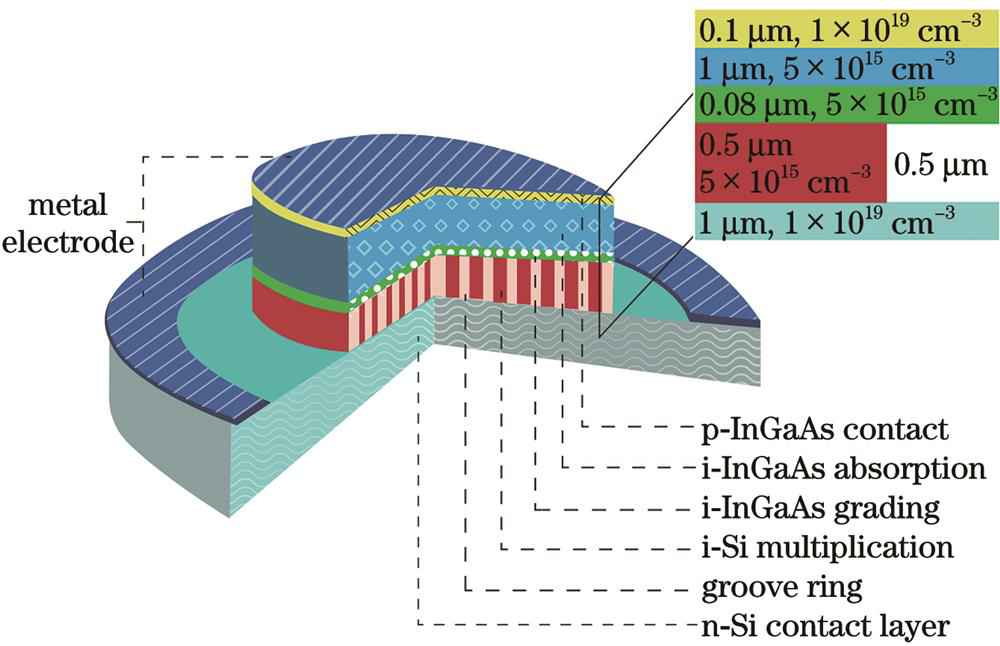
We propose to adopt etching technology to prepare a groove ring within the Si multiplication layer and fill different media inside the groove ring to modulate the electric field in the InGaAs layer and Si layer, which helps build a charge-free layer InGaAs/Si APD device model. Firstly, the changes in APD optical and dark current with different media are simulated. The changes in recombination rate and carrier concentration are simulated to explore the reasons for the changes in optical current. Secondly, the energy band changes of the APD are simulated to further understand the reasons for electron concentration changes. Thirdly, the changes of charge concentration, impact ionization rate, electric field, and other parameters with different media are simulated. Finally, the gain, bandwidth, and gain-bandwidth product of APD are simulated, and a comparison of different media shows that filling with the air can yield the best device performance.
The overall trend of optical current and dark current decreases with the increasing dielectric constant of the medium (Fig. 2). As the dielectric constant of the medium rises, the recombination rate decreases in the InGaAs absorption layer, Si multiplication layer, and Si substrate, consistent with the trend of optical current variation (Fig. 3). The conduction band of APD has no band order at the bonding interface, while the valence band at the interface has obvious band orders, making it difficult for carriers to transport at the interface and a large number of holes to accumulate at the interface (Fig. 5). The ionization coefficients of electrons and holes in the absorption layer slowly increase, while the ionization coefficients of electrons and holes in the multiplication layer further decrease, which is consistent with the trend of electric field changes (Fig. 7). As the dielectric constant increases, the electric field strength in the multiplication region gradually reduces, which weakens the carrier impact ionization effect and decreases the gain (Fig. 8). When the bias voltage is 35 V, the gain-bandwidth product basically shows a downward trend with the increasing dielectric constant of the medium. Additionally, when the medium inside the groove ring is air and the reverse bias voltage is equal to the avalanche voltage (35.2 V), the gain-bandwidth product reaches 100 GHz (Fig. 11).
We investigate the effect of filling different media in the Si multiplication layer groove ring on the charge-free layer InGaAs/Si APD. The results show that as the dielectric constant of different media increases, both optical current and dark current present a decreasing trend under the same bias voltage. The InGaAs/Si APD with air or SiO2 as the dielectric materials finally overlaps with the optical current and dark current after reaching the avalanche voltage, exhibiting the best current characteristics. As the dielectric constant of the medium rises, the gain-bandwidth product shows a downward trend under the same bias voltage. After the device avalanche, the gain-bandwidth product exhibits a trend of first increasing and then decreasing. When the medium inside the groove ring is air and the reverse bias voltage is 35.2 V, the gain-bandwidth product reaches 100 GHz. In summary, replacing the charge layer with a groove ring to construct a charge-free layer InGaAs/Si APD does not require ion implantation, and the process is simple. Meanwhile, filling the groove ring with air can yield the best device performance, and this new configuration provides a new idea for designing high-performance InGaAs/Si APD with simple processes.
张娟, 姚儿, 柯少颖. 无电荷层InGaAs/Si雪崩光电探测器的优化设计[J]. 光学学报, 2024, 44(5): 0504001. Juan Zhang, Er Yao, Shaoying Ke. Optimal Design of Charge-Free Layer InGaAs/Si Avalanche Photodetector[J]. Acta Optica Sinica, 2024, 44(5): 0504001.


