Opto-Electronic Science, 2023, 2 (12): 230017, Published Online: Mar. 19, 2024  

Integrated photonic convolution acceleration core for wearable devices

Author Affiliations
1 Wuhan National Laboratory for Optoelectronics, Huazhong University of Science and Technology, Wuhan 430074, China
2 Optics Valley Laboratory, Wuhan 430074, China
Abstract
With the advancement of deep learning and neural networks, the computational demands for applications in wearable devices have grown exponentially. However, wearable devices also have strict requirements for long battery life, low power consumption, and compact size. In this work, we propose a scalable optoelectronic computing system based on an integrated optical convolution acceleration core. This system enables high-precision computation at the speed of light, achieving 7-bit accuracy while maintaining extremely low power consumption. It also demonstrates peak throughput of 3.2 TOPS (tera operations per second) in parallel processing. We have successfully demonstrated image convolution and the typical application of an interactive first-person perspective gesture recognition application based on depth information. The system achieves a comparable recognition accuracy to traditional electronic computation in all blind tests.

1 Introduction

Wearable devices, characterized by their portability and strong human interaction capabilities, have long represented the future of technology and innovation1. Within the realm of wearable devices, numerous recognition tasks rely on machine vision, such as vehicle detection2, human pose recognition3-6, and facial recognition2, 7-9. These applications primarily rely on the forward propagation of deep learning algorithms to accomplish classification and recognition tasks. However, as the complexity of these applications increases10, the demand for computational power, low power consumption, low heat generation, and high efficiency in wearable devices becomes increasingly challenging to traditional electronic computing because Moore's Law is reaching its limits11. As a result, alternative solutions are imperative.

In recent years, research on optical neural networks (ONNs) has emerged as a potential breakthrough solution to address the bottlenecks of electronic computing12, 13. By mapping the mathematical models of neural networks to analog optical devices, ONNs can achieve computational capabilities superior to electronic computing because optical transmission networks offer the potential for ultra-low power consumption and minimal heat generation14. This makes them well-suited for meeting the energy consumption and heat dissipation requirements of wearable devices. Several ONN architectures have been reported in current researches, including diffractive spatial light networks (DNNs)15-17, wavelength division multiplexing (WDM) based on fiber dispersion18,19, and array modulation using Mach-Zehnder interferometers (MZIs)20-23. While diffractive optical network elements have a large scale of neurons, they are typically bulky and not suitable for integration, and the refresh rate is low. Fiber dispersion-based wavelength division multiplexing schemes also face challenges in the miniaturization of long fiber and precise control of delay dispersion in large-scale networks. Although MZI devices can be implemented for on-chip integration, their relatively large footprint does not provide a significant advantage for large-scale expansion. None of these methods offer substantial advantages in meeting the requirements of future wearable devices. In contrast, the array-based approach using micro-ring resonator (MRR) devices exhibits several advantages that are well-aligned with the breakthrough requirements in wearable device research. MRR arrays are compact and easily integrated, allowing for high-precision and complex calculations through one-to-one assignment during parameter configuration24-26. This makes them suitable for small-size and large-scale applications, meeting the demands of current wearable device research.

In this work, a viable solution has been proposed to address the power consumption and computational speed limitations in wearable devices. The solution is based on an integrated photonic convolution acceleration core (PCAC) with a reconfigurable MRR array that has self-calibration functionality27.

Combined with field programmable gate array (FPGA) control, we utilized this system to conduct parallel convolution for edge detection experiments. Subsequently, we shifted our focus to a typical application in the wearable device domain: first-person perspective gesture recognition tasks. This system enables high-speed computation with 7-bit precision when PCAC chip loading weights, and achieves the same accuracy as traditional electronic computation in blind testing for gesture recognition. It provides an effective approach for wearable devices to achieve complex computational tasks accurately and efficiently while ensuring low power consumption and miniaturization.

2 Results

2.1 The principle
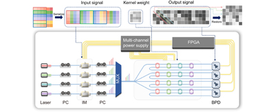
Figure 1 illustrates the principle of the convolutional acceleration system. The proposed convolution acceleration system is capable of performing the multiplication and addition operations of a matrix A of M×N and a vector B of N×1. The vector B is composed of N channels of light signals with different wavelengths. These signals are encoded using an intensity modulator array, where each channel is loaded with a different intensity of light signal. Specifically, for convolving an image with a 4×4 convolutional kernel, we take the image and arrange its elements in groups of four at each row, transposing them into column vectors. These column vectors serve as the encoded information input to the modulators, which are then fed into the PCAC chip. Within the PCAC chip, each column vector is multiplied and summed with the corresponding four MRRs in each row, producing the convolution operation results. The input data then slides down by one stride step, and the next set of four elements is extracted and transposed as the next input signal, continuing the operation with the PCAC chip. We repeat this process and encode all the extracted data into four data streams, which serve as the input for the intensity modulators. The multiplexed signals are then coupled into the PCAC chip through optical fiber. In the PCAC chip, the M×N MRR array is utilized, where each element of matrix A corresponds to an MRR operating at a different resonant wavelength. Under the operation of our developed self-calibrated MRR array, the final computation result is obtained by weighted summation using balanced photodetectors (BPDs), yielding the difference of optical power as the output vector C. The convolution result can be obtained by recovering the data with the assistance of FPGA. During the data recovery and reconstruction process, since each input column vector in the PCAC chip undergoes a simultaneous multiplication and accumulation operation with all rows of the convolutional kernel, the results of the computational operations need to be summed along the diagonal to obtain a single element of the actual convolution result, and this represents the completion of one convolution operation. It is worth noting that due to the one-to-one correspondence between the MRR array and the matrix elements, it is theoretically possible to simultaneously configure multiple convolution kernels and perform convolution operations on data streams representing multiple images. This scalability provides excellent support for large-scale parallelism in optoelectronic computation. Further details of the experiments will be discussed in subsequent sections.

Fig. 1. Schematic of a computing system based on the integrated convolution acceleration core (PCAC) chip.

下载图片 查看所有图片

2.2 The fabrication and characterization of PCAC chip
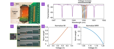
Figure 2(a) shows the PCAC chip, which is fabricated using a typical 220 nm silicon-on-insulator (SOI) integration process, a standard technique in chip manufacturing. This proof-of-concept chip has a compact size of 2.6 mm × 2.0 mm, comprising a 4×4 array of MRR synapses, forming the core of the computing system. These synapses play a crucial role in the chip's computational power. Additionally, a thermally tunable MRR with TiN (titanium nitride) heaters acts as the computational control module of the PCAC chip. This tunable MRR enables precise manipulation of the resonance wavelength, a critical aspect for accurate calculations. To facilitate accurate voltage control of the MRR synapses, meticulous design considerations have been incorporated. We implement specifically tailored FPGA circuit for the chip's requirements, along with a high-resolution digital-to-analog converter circuit capable of programmable voltage outputs at a remarkable 16-bit resolution, enables fine-grained control of the MRR synapses. In order to ensure stability and reliability, the chip incorporates a thermo-electric cooler (TEC) module at its base. This TEC module plays a pivotal role in maintaining a stable temperature environment for the chip, further enhancing the accuracy of its computations. On the left side of the chip, an optical signal output module is meticulously designed, featuring fiber optic packaging for seamless integration with external systems.

Fig. 2. (a) Detailed photos of the packaged layout chip show the MRR array in the center, with the photonics chip on the right combined with the leads of the customized printed circuit board (PCB) for computation and control. On the left, there is an optical input/output port using a fiber V-groove, and the entire assembly is mounted on a TEC for heat dissipation. (b) The micrograph of the MRR array and detailed photo of a single MRR. (c) The transmission spectra of the MRR array. Different voltages (800–1800 mV, 100 mV/step) are applied to the third MRR. Similar results can be obtained when the voltage is applied to other MRRs. (d) The transmission rate of a single IM on the chip under voltage tuning. These curves represent the normalized W-V mapping. (e) The transmission rate of a single MRR on the chip under voltage tuning. These curves represent the normalized W-V mapping.

下载图片 查看所有图片

Moving to the microscopic level, Fig. 2(b) offers an up-close view of the MRR synapses within the array. Additionally, an enlarged microscopic photograph showcases the intricate details of a single MRR. To facilitate efficient electrical and optical input/output (I/O) connections, the chip's design incorporates advanced packaging techniques. Both wire bonding and fiber array have been thoughtfully integrated, ensuring reliable and high-performance I/O connections for both electrical and optical signals. Figure 2(c) illustrates the tuning curve of the pass-through end of an MRR as a function of applied voltage. Increasing the voltage on the MRR leads to a redshift in the resonance wavelength. It can also be observed that when changing the resonance peak of one MRR, the transmission spectra of the other MRRs remain almost unchanged. This indicates that the crosstalk between the MRRs in the array during precise tuning is negligible. To ensure the computational precision of the PCAC chip, we have developed a self-calibration procedure that works in conjunction with the circuit hardware to monitor and calibrate the weights of the on-chip MRRs27. This calibration process enables us to achieve a precision of 7 bits during the actual loading process (specific evaluation criteria can be found in ref.28).

Based on this method, we have established a look-up table for the weight-voltage mapping of the modulator and MRR array. For modulator calibration, the laser operating wavelength is chosen away from the MRR resonance peak for one path of the MRR array. The reference voltage of the MRR array is fixed, and the voltage applied to the modulator is incrementally adjusted in a step of 0.1 V. The optical power of the pass-through end (THRU) is detected using a balanced photodetector (BPD), allowing the construction of a P-V curve that represents the relationship between power and modulator voltage. After differential and normalization operations, a weight-voltage (W-V) curve is established that describes the relationship between input data weights and modulator voltage. Figure 2(d) displays the W-V curve obtained from the calibration of one path of the PCAC chip's modulator. For MRR array calibration, the laser operating wavelength is adjusted to a region close to the resonance wavelength of each MRR. The modulator input voltage is kept constant while the MRR tuning voltage is adjusted, causing each MRR to redshift with the laser wavelength. Throughout this process, the optical power of the pass-through end is continuously detected, enabling the construction of a P-V curve that represents the relationship between power and MRR tuning voltage. After differential and normalization operations, a W-V curve is established that describes the relationship between convolutional kernel weights and modulator voltage. Figure 2(e) illustrates the W-V curve obtained from the calibration of one MRR in the PCAC chip.

2.3 Operation for convolution and edge detection

In order to verify the convolutional computing capability of the PCAC chip within our system, we conducted a series of experiments using the widely recognized "cameraman" image as a standard test case. Figure 3(a) provides a comprehensive overview of the experimental setup, illustrating the key components involved in this proof-of-concept study. During the experiment, we employed a 3×3 MRR array as a convolutional kernel weight loading device, perfectly matching the size of the 3×3 convolutional kernel used. The input image, a grayscale image with dimensions of 256×256 pixels, was initially flattened into a one-dimensional vector. To achieve high-speed processing, we adopted an intensive parallel processing approach, where every three elements of the vector were grouped together and loaded onto the intensity modulator (IM). This allowed us to stream the data into the system in a synchronized manner. Once the data was serialized, it was channeled into the PCAC chip, which served as the core processing unit. Within the PCAC chip, each ring was dedicated to a specific convolutional kernel. The input values were fed through the pass-through end (THRU) and underwent multiplication and addition (MAC) operations along each row. Ultimately, the results of the convolutional operations were transmitted to a balanced photodetector via the drop port (DROP), where optical power was acquired for further analysis. Figure 3(b) shows the original image used in the edge detection test, which is a 256×256 pixels image of a cameraman. To better understand the impact of the convolutional kernels, Fig. 3(c) shows three specific types used for edge detection: Bottom sobel, Top sobel, and Left sobel. These kernels were designed to detect vertical and horizontal edges within the image. Figure 3(d) visually presents the outcome of applying these three edge detection operations, representing the result of a single convolutional operation. The experimental results provided substantial evidence to support the effectiveness of utilizing the PCAC chip within an optoelectronic system for parallel convolutional computing.
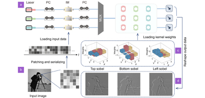
Fig. 3. (a) Experimental setup of the PCAC chip for performing convolutional operations. (b) Original image used for demonstrating the convolution effect. (c) Convolution kernels used: Bottom sobel, Top sobel, Left sobel. (d) Corresponding convolution image results.

下载图片 查看所有图片

2.4 Application of first-person depth-based gesture recognition using PCAC chip

In this part, we further explore its performance in practical applications for devices. First-person perspective gesture recognition is one of the most widespread applications for wearable devices, such as virtual reality (VR) and augmented reality (AR) glasses, Remote Healthcare Monitoring devices29. Taking this into account, we have developed a digital gesture recognition application that incorporates depth information, specifically designed for wearable devices. This application is capable of recognizing hand gestures representing digits from 0 to 9. We utilized the EgoGesture dataset30, released by the Institute of Automation, Chinese Academy of Sciences in 2017. Each gesture was represented by 1500 training images and 300 testing images, resulting in a total of 18000 images as our dataset. We trained the artificial intelligence model on a computer. Figure 4(a) illustrates the main structure of the convolutional neural network (CNN) used in our application. Depth images captured by the SR300 depth camera were used as input data, with a gesture image size of 32×32×1. The first layer consisted of 16 convolutional kernels, each with a size of 3×3. The convolutional operations were performed entirely by the PCAC chip. Similar to the previous experiments, input images were reshaped into three rows of data and streamed into the PCAC chip, where they were convoluted with the loaded kernels. After one convolutional layer, the output size became 30×30×16. With the assistance of a computer system, the output data were processed by the activation function (ReLU) and then injected into a pooling layer for downsampling. Subsequently, two more convolutional layers, maximum pooling layers, and fully connected layers were applied, resulting in the final recognition of the 0–9 numeral gestures. Figure 4(b) displays a bar graph showing the recognition results of the ten gestures calculated by the PCAC chip. The horizontal axis represents the ten gestures, while the vertical axis represents the probability of recognizing each numeral. In the 10 recognition samples for digits 0–9, except for digits 2, 3, and 8, where there are probability distributions with both main and secondary peaks, the rest of the digits show single peak recognition. This indicates that the PCAC chip enables accurate recognition tasks. It is worth noting that for electronic computation, the model achieves a recognition accuracy of 91.14% in blind testing. Similarly, when using the PCAC chip for optoelectronic computation, all the blind test images yield the same recognition accuracy as those obtained through electronic computation. The graph demonstrates that the PCAC chip successfully implemented convolutional operations and achieved accurate recognition of depth-based numeral gestures.
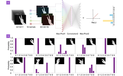
Fig. 4. (a) Schematic diagram of the convolutional neural network (CNN) architecture suitable for first-person digit gesture recognition with depth information. (b) Probability of recognition for the 10 gestures after performing the convolutional layer computation using the PCAC chip as a replacement for the computer.

下载图片 查看所有图片

To further investigate the performance of the PCAC chip in computational tasks, we conducted a more detailed analysis of the experimental results. Figure 5(a) compares the experimental results obtained by performing convolutional calculations using PCAC and the theoretical results obtained using digital computers for the recognition of Gesture 2. The scatter points exhibit a tight distribution along the diagonal line, which corresponds to the theoretical expectations. Figure 5(b) displays a histogram showing the probability distribution of the offsets (experimental values minus theoretical values) for all data points. The histogram exhibits a distribution similar to a Gaussian distribution, with the highest probability of offset near zero. Figure 5(c) shows the recorded offsets for each calculation sample during the computation process. The offsets are mostly distributed around zero and exhibit a stable and uniform distribution without significant fluctuations. Figure 5(d) and 5(e) provide visual comparisons between the theoretical results (computed by a computer) and the experimental results (obtained using the PCAC chip) after the first-layer convolutional operation specifically for the gesture representing the numeral 2. Apart from some variations in background color caused by experimental noise, the results obtained by the PCAC chip for convolutional computations are nearly identical to those obtained by the computer. In summary, the analysis reveals that the PCAC chip demonstrates high accuracy and stability in computational tasks when compared to theoretical calculations. The visual comparisons also confirm the consistency between the results obtained by the PCAC chip and those obtained by a conventional computer. These findings underscore the potential of the PCAC chip as a viable alternative for accelerating and improving recognition and classification tasks.
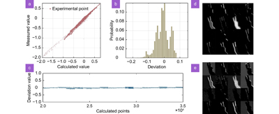
Fig. 5. (a) Scatter plot comparing measured results with calculated results for Gesture 2. (b) Probability distribution of the error offset in the experimental results, resembling a Gaussian curve. (c) Offset of each point during the computation process. (d) Results of the first layer convolution computation obtained through electronic computation. (e) Results of the first layer convolution computation obtained through optical-electronic computation using the PCAC chip.

下载图片 查看所有图片

3 Discussion

3.1 Energy efficiency estimation

Benefiting from the compact size of MRR resonators, the PCAC chip achieves high integration density within a footprint of just 0.2 mm2. In the meantime, it enables basic multiplication and addition operations with same recognition results as electronic computation. For a 4×4 scale PCAC chip with four parallel channels, the footprint increases to approximately 5 square millimeters, allowing for parallel convolution operations and efficient processing of more complex computational recognition tasks. However, despite these advantages, the PCAC chip design still has limitations and potential areas for improvement.

Firstly, the eternal pursuit of photonic computation lies in processing data with high speed and low power consumption. In our concept verification setup, the power consumption is primarily attributed to the laser, silicon photonic chip, modulator, TEC, and digital backend. Based on the components utilized in our measurement setup, the estimated power consumption in the computation system is approximately 7.716 W, resulting in a total power consumption of around 40.973 W. Consequently, 80% of the power is attributed to these benchtop instruments. Table 1 shows the details of power consumption.

Table 1. Estimated power consumption of the proof-of-concept system.

ComponentsVoltage(V)Current(A)Power(W)
Lasers~10×10-3×4=0.04
On ring heatersV¯2~5×10⁻³~0.01×16=0.16
Intensity modulator1V¯70.2661.862
Intensity modulator2V¯6.50.2781.807
Intensity modulator3V¯70.2721.904
Intensity modulator4V¯7.50.2591.943
System’s power consumption7.716
TEC for PCAC chip6.1450.533.257
CPU~30
Total power consumption40.973

查看所有表

Using phase-change materials as thermal shifters can further optimize the energy efficiency of the system. With the development of tunable optical frequency combs31-33, replacing lasers with microcombs as light sources can significantly reduce power consumption. This will unlock the full potential of the optoelectronic computing system, offering higher scalability, higher integration, and lower power consumption. It is important to note that with the development of hybrid integration and monolithic integration techniques, advancements in light sources, silicon photonic circuits, and related electronic components (including modulators, drivers, trans-impedance amplifiers (TIA), digital-to-analog converters (DAC), and analog-to-digital converters (ADC)) can be integrated onto the same motherboard or even onto a single chip. This integration trend has the potential to significantly reduce power consumption. Therefore, the power and integration performance demonstrated in this work have the potential for further enhancement, although there is still a long road ahead.

3.2 Throughput estimation

Furthermore, as a key metric for evaluating computational hardware performance, throughput is defined as the number of operations per second (OPS) performed by a processor in high-performance computing (HPC) domain. The throughput of photonic computing hardware can be calculated using Eq. (1)20:

T(OPS)=2m×N2×r,

where T represents the throughput in OPS (operations per second) excluding the time spent on off-chip signal loading during photonic computation, m is the number of layers implemented by the photonic computing hardware, N2 is the size of the on-chip weight library, and r is the detection rate of the photodetector (PD). Since the PCAC chip can naturally perform multiplication and addition (MAC) operations, and each MAC operation consists of one multiplication and one addition operation, one MAC operation corresponds to two operations. With a typical photodetection rate of 100 GHz, our PCAC concept validation chip (N2=4×4) can achieve 3.2 TOPS, which still lags behind leading electronic processors such as Google's tensor processing unit (TPU)34 and other chips. However, due to the chip's strong scalability, in future large-scale chips of 16×16 dimensions with auxiliary optical frequency combs as multiple light sources is possible to reach the theoretical computational power of 51.2 TOPS. This will enable outstanding performance in complex computational tasks with ultra-high integration and ultra-low power consumption, helping to alleviate the high cost of electronic computing while ensuring high computational power. It serves as an effective solution for breakthroughs in the field of wearable devices. Although, there are various challenges in photonic computing that include limitations posed by components such as ADCs, DACs, modulators, PDs, in terms of their speed and bandwidth. While these challenges are not the primary focus of our current work, they are certainly within the broader scope of the field. We believe that with concerted efforts from the entire photonic computing community, these challenges can be addressed and overcome. As the field progresses, it is reasonable to expect advancements that will lead to breakthroughs in addressing the speed and bandwidth limitations of photonic components.

3.3 Scalability

To further improve the computational performance of PCAC chips, ensuring scalability is an extremely important requirement. The main source of losses in PCAC chip arises from the coupling gratings. Therefore, the scalability of PCAC chip is not primarily limited by its loss performance. Instead, it is predominantly determined by the free spectral range (FSR) of each MRR. Since each MRR requires individual tuning, and precision is essential to avoid resonance overlap during thermal tuning for high-precision computations, the scalability within a given operational wavelength range is somewhat constrained. This constraint emerges as we conduct experiments within a specific wavelength range. Our future endeavors are aimed at addressing this limitation by designing MRR with larger FSR. This design approach will enable the development of larger-scale PCAC chips operating with a greater range of wavelengths, thereby delivering enhanced computational performance. Ultimately, this advancement will expand the horizons for exploring more complex applications in the field, offering a broader spectrum of possibilities.

3.4 Wearable application potential

Finally, it is important to note that in this work, we have only showcased one application scenario for wearable devices. In this work, we have successfully demonstrated the capabilities of optical-electrical computation in a practical context by implementing first-person perspective gesture recognition tasks using the PCAC chip and accompanying algorithms (We have provided a demo video in the attachment that showcases the real-time interaction of this application). Unlike previous tests limited to MNIST handwritten digit recognition (with small input images and a few convolutional kernels), our application involves larger input images (32×32 pixels) and a more intricate network structure (with a first-layer convolution containing 16 kernels). These factors pose a greater challenge to the sustained high-precision computational capability of the photonic chip. The successful completion of the recognition task demonstrates the photonics hardware's capacity to handle such complex tasks. Compared to the previous tasks involving simple MNIST digits or edge detection, this work holds higher practical value due to its ability to address more intricate recognition tasks. However, the photonic convolution acceleration core computational system presented here can be applied to various scenarios involving convolution operations. Especially when considering the inherent advantages of photonics such as low power consumption and minimal heat generation, which align perfectly with the requirements of wearable devices. Building upon the previously mentioned approaches, further optimizations can be pursued to enhance integration, energy efficiency, and scalability. These improvements aim to achieve higher computational power while maintaining efficiency and compactness. We believe that this computational system has the potential to play a significant role in a broader range of wearable device applications.

4 Conclusions

In this work, we propose a convolutional acceleration processor based on an MRR array and have successfully fabricated a prototype PCAC chip. When combined with the computational control module programmed on an FPGA, the PCAC chip is capable of performing convolution operations with a maximum precision of 7 bits. We demonstrate the application of the PCAC chip in complex gesture recognition tasks, specifically in first-person depth information gesture recognition. With parallel and precise convolution operations, we obtain the same recognition results as traditional electronic computation in all blind tests, achieving a high level of recognition accuracy. The outstanding performance in accomplishing complex recognition tasks and high-precision forward propagation tasks opens up new possibilities for intuitive human-machine interaction. Furthermore, the advantages of optical computation, including reduced power consumption and faster data processing, make this application particularly important in the development of wearable devices. Accurate and efficient gesture recognition enables seamless control and interaction with the device, enhancing user experience and convenience. Additionally, the compact and easily integrable nature of the device provides opportunities for higher computational power and lower power consumption in future large-scale expansions. These advantages offer an effective solution to address the challenges of heat dissipation and integration in wearable devices when dealing with complex, high-precision, multi-scenario computational recognition tasks. It paves the way for efficient computation by effectively surpassing the limitations of electronic processors.

5 Acknowledgements

This work was partially supported by the National Natural Science Foundation of China (U21A20511), the Innovation Project of Optics Valley Laboratory (OVL2021BG001).

BH Zhao and JW Cheng proposed the original idea, JJ Dong supervised the project, BH Zhao fabricated the chip and performed the measurements, all authors contributed to the writing of the article.

The authors declare no competing financial interests.

Attachment video.https://doi.org/10.29026/oes.2023.230017

References

[1] ZhangSB, LiYX, ZhangS, ShahabiF, XiaSet al. Deep learning in human activity recognition with wearable sensors: a review on advancesSensors202222147610.3390/s22041476

[2] ChangWJ, ChenLB, ChiouYZ. Design and implementation of a drowsiness-fatigue-detection system based on wearable smart glasses to increase road safetyIEEE Trans Consum Electron20186446146910.1109/TCE.2018.2872162

[3] RamanujamE, PerumalT, PadmavathiS. Human activity recognition with smartphone and wearable sensors using deep learning techniques: a reviewIEEE Sensors J202121130291304010.1109/JSEN.2021.3069927

[4] ChenKX, ZhangDL, YaoLN, GuoB, YuZWet al. Deep learning for sensor-based human activity recognition: overview, challenges, and opportunitiesACM Comput Surv2022547710.1145/3447744

[5] WangJD, ChenYQ, HaoSJ, PengXH, HuLS. Deep learning for sensor-based activity recognition: a surveyPattern Recognit Lett201911931110.1016/j.patrec.2018.02.010

[6] NwekeHF, TehYW, Al-garadiMA, AloUR. Deep learning algorithms for human activity recognition using mobile and wearable sensor networks: state of the art and research challengesExpert Syst Appl201810523326110.1016/j.eswa.2018.03.056

[7] TervenJR, RaducanuB, Meza-de-LunaME, SalasJ. Head-gestures mirroring detection in dyadic social interactions with computer vision-based wearable devicesNeurocomputing201617586687610.1016/j.neucom.2015.05.131

[8] Perusquía-HernándezM, HirokawaM, SuzukiK. A wearable device for fast and subtle spontaneous smile recognitionIEEE Trans Affective Comput2017852253310.1109/TAFFC.2017.2755040

[9] GrueblerA, SuzukiK. Design of a wearable device for reading positive expressions from facial EMG signalsIEEE Trans Affective Comput2014522723710.1109/TAFFC.2014.2313557

[10] BrownTB, MannB, RyderN, SubbiahM, KaplanJet al. . Language models are few-shot learners. In Proceedings of the 34th International Conference on Neural Information Processing Systems159 (ACM, 2020); http://doi.org/10.5555/3495724.3495883.

[11] HusseinAI. . Wearable computing: challenges of implementation and its future. In 2015 12th Learning and Technology Conference14–19 (IEEE, 2015);http://doi.org/10.1109/LT.2015.7587224.

[12] ZhouHL, DongJJ, ChengJW, DongWC, HuangCRet al. Photonic matrix multiplication lights up photonic accelerator and beyondLight Sci Appl2022113010.1038/s41377-022-00717-8

[13] ShastriBJ, TaitAN, Ferreira De LimaT, PerniceWHP, BhaskaranHet al. Photonics for artificial intelligence and neuromorphic computingNat Photonics20211510211410.1038/s41566-020-00754-y

[14] NahmiasMA, De LimaTF, TaitAN, PengHT, ShastriBJet al. Photonic multiply-accumulate operations for neural networksIEEE J Sel Top Quantum Electron20202611810.1109/jstqe.2019.2941485

[15] LinX, RivensonY, YardimciNT, VeliM, LuoYet al. All-optical machine learning using diffractive deep neural networksScience20183611004100810.1126/science.aat8084

[16] PanuskiCL, ChristenI, MinkovM, BrabecCJ, Trajtenberg-MillsSet al. A full degree-of-freedom spatiotemporal light modulatorNat Photonics20221683484210.1038/s41566-022-01086-9

[17] LiJX, HungYC, KulceO, MenguD, OzcanA. Polarization multiplexed diffractive computing: all-optical implementation of a group of linear transformations through a polarization-encoded diffractive networkLight Sci Appl20221115310.1038/s41377-022-00849-x

[18] XuXY, TanMX, CorcoranB, WuJY, BoesAet al. 11 TOPS photonic convolutional accelerator for optical neural networksNature2021589445110.1038/s41586-020-03063-0

[19] BaiBW, YangQP, ShuHW, ChangL, YangFHet al. Microcomb-based integrated photonic processing unitNat Commun2023146610.1038/s41467-022-35506-9

[20] ShenYC, HarrisNC, SkirloS, PrabhuM, Baehr-JonesTet al. Deep learning with coherent nanophotonic circuitsNat Photonics20171144144610.1038/nphoton.2017.93

[21] HughesTW, MinkovM, ShiY, FanSH. Training of photonic neural networks through in situ backpropagation and gradient measurementOptica2018586487110.1364/OPTICA.5.000864

[22] ZhouHL, ZhaoYH, WangX, GaoDS, DongJJet al. Self-configuring and reconfigurable silicon photonic signal processorACS Photonics2020779279910.1021/acsphotonics.9b01673

[23] ZhangH, GuM, JiangXD, ThompsonJ, CaiHet al. An optical neural chip for implementing complex-valued neural networkNat Commun20211245710.1038/s41467-020-20719-7

[24] TaitAN, De LimaTF, ZhouE, WuAX, NahmiasMAet al. Neuromorphic photonic networks using silicon photonic weight banksSci Rep20177743010.1038/s41598-017-07754-z

[25] XuSF, WangJ, YiSC, ZouWW. High-order tensor flow processing using integrated photonic circuitsNat Commun202213797010.1038/s41467-022-35723-2

[26] HuangCR, BilodeauS, Ferreira De LimaT, TaitAN, MaPYet al. Demonstration of scalable microring weight bank control for large-scale photonic integrated circuitsAPL Photonics2020504080310.1063/1.5144121

[27] ChengJW, HeZM, GuoYH, WuB, ZhouHLet al. Self-calibrating microring synapse with dual-wavelength synchronizationPhotonics Res20231134710.1364/PRJ.478370

[28] ZhangWP, HuangCR, PengHT, BilodeauS, JhaAet al. Silicon microring synapses enable photonic deep learning beyond 9-bit precisionOptica2022957958410.1364/OPTICA.446100

[29] BandiniA, ZariffaJ. Analysis of the hands in egocentric vision: a surveyIEEE Trans Pattern Anal Mach Intell2023456846686610.1109/TPAMI.2020.2986648

[30] ZhangYF, CaoCQ, ChengJ, LuHQ. EgoGesture: a new dataset and benchmark for egocentric hand gesture recognitionIEEE Trans Multimedia2018201038105010.1109/TMM.2018.2808769

[31] RazzariL, DuchesneD, FerreraM, MorandottiR, ChuSet al. CMOS-compatible integrated optical hyper-parametric oscillatorNat Photonics20104414510.1038/nphoton.2009.236

[32] MossDJ, MorandottiR, GaetaAL, LipsonM. New CMOS-compatible platforms based on silicon nitride and Hydex for nonlinear opticsNat Photonics2013759760710.1038/nphoton.2013.183

[33] KippenbergTJ, GaetaAL, LipsonM, GorodetskyML. Dissipative kerr solitons in optical microresonatorsScience2018361eaan8083

[34] GravesA, WayneG, ReynoldsM, HarleyT, DanihelkaIet al. Hybrid computing using a neural network with dynamic external memoryNature201653847147610.1038/nature20101

Baiheng Zhao, Junwei Cheng, Bo Wu, Dingshan Gao, Hailong Zhou, Jianji Dong. Integrated photonic convolution acceleration core for wearable devices[J]. Opto-Electronic Science, 2023, 2(12): 230017.
引用该论文: TXT   |   EndNote

相关论文

加载中...

关于本站 Cookie 的使用提示

中国光学期刊网使用基于 cookie 的技术来更好地为您提供各项服务,点击此处了解我们的隐私策略。 如您需继续使用本网站,请您授权我们使用本地 cookie 来保存部分信息。
全站搜索
您最值得信赖的光电行业旗舰网络服务平台!