Nanobridged rhombic antennas supporting both dipolar and high-order plasmonic modes with spatially superimposed hotspots in the mid-infrared
1 Introduction
Mid-infrared antennas (MIRAs), often constructed from metals (e.g., Au, Al or Ag), highly doped III-V semiconductors, electron-doped graphene or phonon-polariton-based nanostructures1-11, support optical resonance in the mid-infrared spectral range (400 to 4000 cm–1). MIRAs can act as receiving antennas thereby concentrating mid-infrared beams from free space to nanoscale regions (termed as hotspots) in the vicinity of the surface of MIRAs12. MIRAs can also act as transmitting antennas to directionally amplifying thermal radiation produced by local heating of sources coupled to MIRAs13. These impressive features of MIRAs have inspired a wide range of investigation of their potential applications for surface-enhanced infrared absorption (SEIRA) spectroscopy leading to ultrahigh sensitivities (up to hundreds of oscillators)14, for biological and chemical sensors in the mid-infrared region15-18, for beam-shape engineering of quantum cascade lasers (QCL)19, and for highly-responsive photodetectors20 with enhanced absorption and photocarrier collection efficiency in the mid-infrared21. The core elements for the high-performance applications are the MIRA micro- and nanostructures, but the development of MIRA structures lags far behind that of optical antenna nanostructures in the visible spectral range22.
Single-arm dipolar-antenna structures are among the most classical MIRAs, often consisting of gold rods with tunable resonant wavelengths by tuning the length of the rods23-26. Furthermore, dual-arm dipolar-antennas with nanometer-sized gaps (nanogaps), such as gold rod dimers, have also been developed on account of the strength of the local field enhancement factors (LFEFs, |
To obtain multiband MIRAs, several micro- and nanostructures beyond single-arm or dual-arm antennas have been designed, among them, gold nano-crosses32, 33, nanoaperture structures34, 35, fractal microstructures36-38, log-periodic trapezoidal structures39, and dipolar antennas with multiple lengths40-42. These structures could be categorized into the micro- and nanostructures supporting several dipolar modes. Fundamentally, it is a long-term challenge to develop single-arm or dual-arm antennas supporting simultaneously pronounced fundamental and high-order plasmonic modes such as a quadrupolar mode.
In this study, we develop a nanobridged rhombic antenna (NBRA) exhibiting two pronounced resonance-bands in the MIR regions. The two bands are assigned to a charge-transfer plasmon (CTP) mode and a bridged dipolar plasmon (BDP) mode, which are demonstrated by the scattering-type scanning near-field optical microscopy (s-SNOM), a technique that is widely used to image the near-field distribution of plasmonic modes43-47. The nanobridge structure and the linked rhombic-arm antennas effectively controls the resonant frequencies and extinction intensities of the CTP and BDP bands. The s-SNOM also demonstrates that the main hotspots of the two bands are spatially overlapped. This feature enables us to boost up the local field enhancement of both bands via NBRA dimers with nanogaps. Moreover, one order of magnitude of additional enhancement can be obtained for both bands from a hybrid structure consisting of an NBRA dimer, a sandwiched dielectric spacer layer and a gold reflector. Such high field enhancement enables detecting a monolayer of molecules using the two absorptions located in the two bands.
2 Materials and methods
2.1 Numerical simulations
All electromagnetic simulations were performed by the commercial software COMSOL Multiphysics based on the finite element method. The simulation space was a cuboid, whose sizes along the long and short axes of the NBRA were equal to the fabricated arrays. The perfectly matched layers were used for the top and bottom boundaries while the periodic conditions were employed for the side boundaries. The polarization of the incident electric field was either parallel or perpendicular to the long axis of the antenna and the resulting transmittance or reflectance spectra were averaged to approximate the unpolarized illumination used in the experiment. Corners and edges of the gold nanostructure were rounded by a radius of 10 nm for a reasonable simulated local-field distribution there. The mesh size was set as 0.5 nm for each dimension of the nanostructure and its close proximity and gradually became coarser toward the outer borders of the simulation domain. The mesh sizes of different parts are listed in
Table S1. The convergence condition is satisfied (
Fig. S2, Supplementary information). All the |
2.2 Fabrication of NBRAs
All the NBRAs were fabricated on the CaF2 substrate or on the reflective substrate by sequentially using electron-beam lithography, metal deposition and “Sketch and Peel” lithography (SPL)49-53. First, a hydrogen silsequioxane (HSQ) resist (XR−1541-006, Dow Corning) was spin-coated on the substrate at the speed of 4000 rpm. Then, a conductive polymer (ESPACER, Showa Denko) layer of 30 nm was casted on the HSQ resist to avoid pattern distortions due to the charging effect. The sample was then directly loaded into electron-beam direct writing system (Raith 150 Two). The exposure was executed by an electron beam with an accelerating voltage of 30 kV and a beam current of 280 pA. Before the development, the top layer of conductive polymer should be removed by DI water for 10 s, and then a salty developer (1%wt NaOH + 4%wt NaCl aqueous solution) was used to chemically etch the unexposed HSQ resist for 1 min. To stop further development, the structured substrate was immediately rinsed by DI water. The dipping in isopropanol reduced the surface tension and further helped us to obtain the upright HSQ thin-wall structures on the substrate after blow-drying of nitrogen gas steam.
Metal deposition was applied by a thermal evaporation system. The working chamber was pre-pumped to the pressure of 1 × 10⁻⁵ Pa, and the working pressure was kept at the value of 5 × 10⁻⁵ Pa. Due to the requirement of peeling off gold film, the deposition of adhesive metal was excluded from our fabrication process. A 30-nm thick gold film was obtained at a rate of 5 angstrom/s. The thickness was monitored by a quartz-crystal microbalance possessing the sensitivity of angstrom.
The standard process of SPL was reported in our previous literature49-53. To figure out the influence of HSQ in optical measurement, a vapor-HF chemical etching was used to remove HSQ templates. To avoid the condensation of H2O byproduct in etching, the sample was kept at the temperature of 40°C.
2.3 Scanning electron microscopy
The morphology of resultant substrates was characterized by a field-emission scanning electron microscope (SIMG-HD, Carl-ZEISS). To avoid the charging effect during the imaging process, the accelerating voltage and the working distance were set as 1 kV and 3 mm, respectively.
2.4 FTIR microscopy measurements
A commercial FTIR spectrometer (Thermo Fisher Nicolet iN10) was used to perform all transmittance and reflectance measurements. The instrument is equipped with a silicon carbide (globar) light source, a KBr beam splitter, Cassegrain objective (15×, N.A. = 0.4, incident angle θ ranging between 10 and 44°) and a mercury cadmium-telluride (MCT) detector. The transmittance or reflectance of the antennas were defined as the signal intensities transmitted/reflected from the antenna divided by those from a background taken at a blank area on the substrate. Each spectrum was acquired by averaging 64 spectra with a 3 cm–1 spectral resolution. A 100 × 100 µm2 square collection aperture was used for all the measurements. The SEIRA spectra were obtained by subtracting the baseline (generated by asymmetric least-squares smoothing algorithm)54 from the original data. The incident and collected light are unpolarized light.
2.5 Scattering-type scanning near-field optical microscopy (s-SNOM) measurement
The s-SNOM system (neaspec GmbH) was employed to perform the near-field amplitude and phase imaging of the NBRA structures. A silicon atomic force microscopy (AFM) tip (Nanosensors, PPP-NCH) worked as the scatterer to transform the near-field signals to the far field, when the tip and the antenna sample were illuminated by the focused beam of a continuously tunable QCL source. The illuminating beam was incident at ~50° referring to the surface normal, and its polarization was parallel to the long axis of the NBRA structure (s-polarized light). The signals backscattered by the tip were detected with a pseudo-heterodyne interferometer55. The vertical (p-polarized) components of the signals were selected by using a polarizer in front of the detector. To obtain a modulation of the distance between tip and antenna, the tip was oscillating vertically at a frequency Ω≈250 kHz with an amplitude of ~100 nm. Demodulation of the detected signals at the third harmonic frequency (3Ω) yielded almost background-free amplitude and phase signals |s3| and φ3.
2.6 Functionalization with PNTP molecules of the antennas
The sample was incubated in an ethanolic solution of 4-nitrothiophenol (PNTP, 98%, Matrix Scientific) for 12 hours and then was rinsed with a large amount of ethanol (AR, Sinopharm Chemical Reagent Co., Ltd) to remove physically adsorbed molecules, and finally was dried with nitrogen. The concentration of the ethanolic solution of PNTP was kept constant at 1 mM.
3 Results and discussion
3.1 NBRA structure and optical properties
The NBRA (Fig. 1(a, c) and
Fig. S3(a), Supplementary information) consists of two rhombic arms connected with each other by a nanobridge (about 30 nm in width and 130 nm in length). Each arm contains a sharp tip (the corner angle α in Fig. 1(d) is 30°) with a radius of curvature about 10 nm. The thickness (
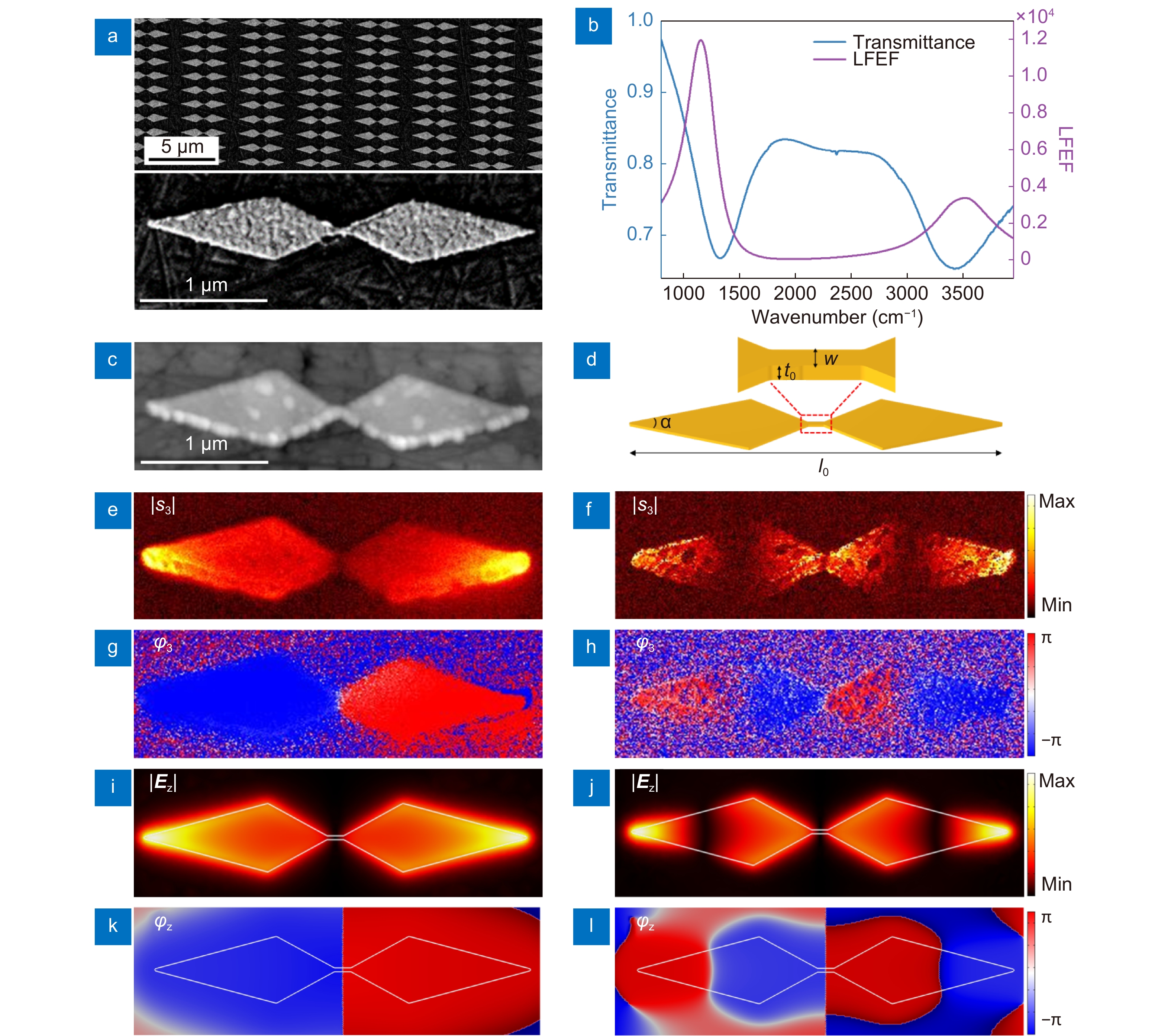
Fig. 1. (a ) Scanning electron microscopy (SEM) image of NBRA structures. (b ) Experimental transmittance of the NBRA array (blue curve) and simulated LFEF at the extremities of the structure (purple curve). (c ) AFM topography of a single NBRA structure. The scale bars are 1 μm. (d ) Sketch and parameters of the NBRA structure, consisting of two rhombic arms connected with each other by a nanobridge. The thickness (t 0) and total length (l 0) of NBRA are 30 nm and 2800 nm. The nanobridge is 30 nm in width and 130 nm in length. The radius of sharp tip of each arm is 10 nm and α is 30°. (e –h ) Measured near-field (e, f) amplitude and (g, h) phase of single NBRA structure at 1100 cm−1 and 2100 cm−1, respectively. (i –l ) Simulated |E φ z (k, l) of single NBRA structure at 1100 cm−1 and 2100 cm−1, respectively.
The measured near-field amplitude image exhibits two hotspots at the two extremities of the structure (Fig. 1(e)) when illuminating with a continuum-wave beam at 1100 cm–1 from the QCL, which is in accord with the simulated |
To assign the plasmonic mode associated with the band centered at 3425 cm–1, we performed the s-SNOM imaging at 2100 cm–1 (4.76 μm) which corresponds to the shortest wavelength of the QCL source in our laboratory. The simulated LFEF at 2100 cm–1 is around 25, which means the s-SNOM signals would be rather weak. In spite of this, the simulated charge distribution (
Fig. S7, Supplementary information) shows similar characteristic between 2100 cm–1 and 3425 cm–1. Thus the s-SNOM imaging still allows us to distinguish the plasmonic mode of this band. The measured near-field amplitude (Fig. 1(f)) and the simulated |
The NBRA excites the high-order mode more efficiently than the nanobar. The extinction spectra of the NBRA and the nanobar monomer both show two resonant bands in the mid-infrared range ( Fig. S9(a), Supplementary information). The extinction intensities of the NBRA at the first and second band are 8.3% and 156.1% larger than those of the nanobar ( Fig. S9(a), Supplementary information). Meanwhile, the resonant wavenumbers of the NBRA are slightly red-shift compared with that of the nanobar. And the full width at half maximum (FWHM) of the resonant bands of the NBRA are broader than those of the nanobar ( Table S2, Supplementary information).
Comparing with other nanobridged structures, such as nanobridged-disks (Fig. 2(b)) or rectangles (Fig. 2(c)), the NBRA (Fig. 2(a)) shows distinct multiband resonances in the mid-infrared region in the simulated extinction spectra (Fig. 2(d)). Further, the hotspots of the NBRA are located at the extremities of the structure (Fig. 2(f)), while the hotspots of nanobridged-disks or rectangles at the CTP resonance are distributed dispersively (Fig. 2(g) and 2(h)), resulting to ten times lower LFEFs than that of the NBRA (Fig. 2(e)).
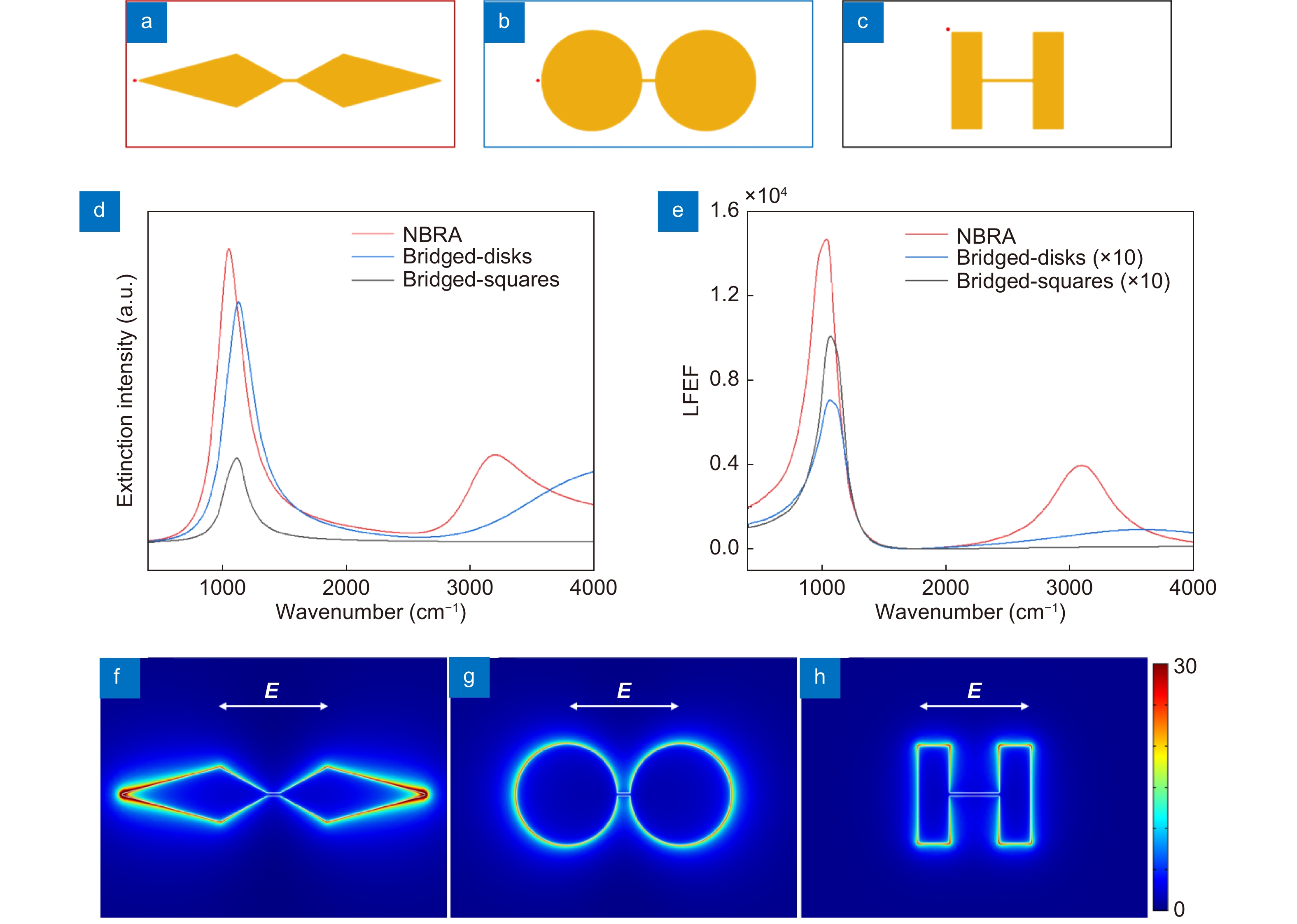
Fig. 2. The model of (a ) NBRA, (b ) nano-bridged disks and (c ) nano-bridged rectangles. All the structures are placed on the CaF2 substrate. The incident polarizations are along the long-axis of the nanobridge. The thickness and the width of the nanobridge are 30 nm for all three structures. The lengths of the nanobridges are 130 nm for the NBRA and the nanobridged-disks, and 500 nm for the nanobridged-rectangles. The total length of the NBRA is 3000 nm. The radius of the disks are 500 nm. The length and width of the rectangles are 962 nm and 308 nm, respectively. The red points in (a–c) are the positions where the LFEFs are evaluated. The LFEF was evaluated at the point 2 nm away from the structure along the long axis and 15 nm above the CaF2 substrate for the NBRA and the nanobridged-disks. While for the nanobridged-rectangles, the evaluating point is 2 nm away from the corner of the rectangle. (d ) The simulated extinction spectra and (e ) the LFEFs of all three structures. E-field distributions at the CTP resonance for (f ) the NBRA, (g ) the nanobridged-disks and (h ) the nanobridged-rectangles.
The CTP and BDP bands of the NBRA are strongly associated with the geometrical parameters of the nanobridge. Figure 3(a) shows that the CTP band redshifts and weakens, and the BDP band redshifts and broadens as the width of the nanobridge decreases from 30 nm to 5 nm. As the nanobridge is broken and transforms to a nanogap in between the two arms, the BDP band disappears in their stead a bonding dipolar plasmonic mode (Fig. 3(b)) and a bonding quadrupolar plasmonic mode (Fig. 3(c)) appears. In contrast, as the width of the nanobridge increases from 30 nm to 370 nm, the CTP band blueshifts and strengthens, and the BDP band blueshifts and weakens. Ultimately, the CTP and BDP bands evolve to a typically dipolar band (Fig. 3(d)) and quadrupolar band (Fig. 3(e)), respectively, similar to that in a nanobar antenna of the same length ( Fig. S10, Supplementary information).
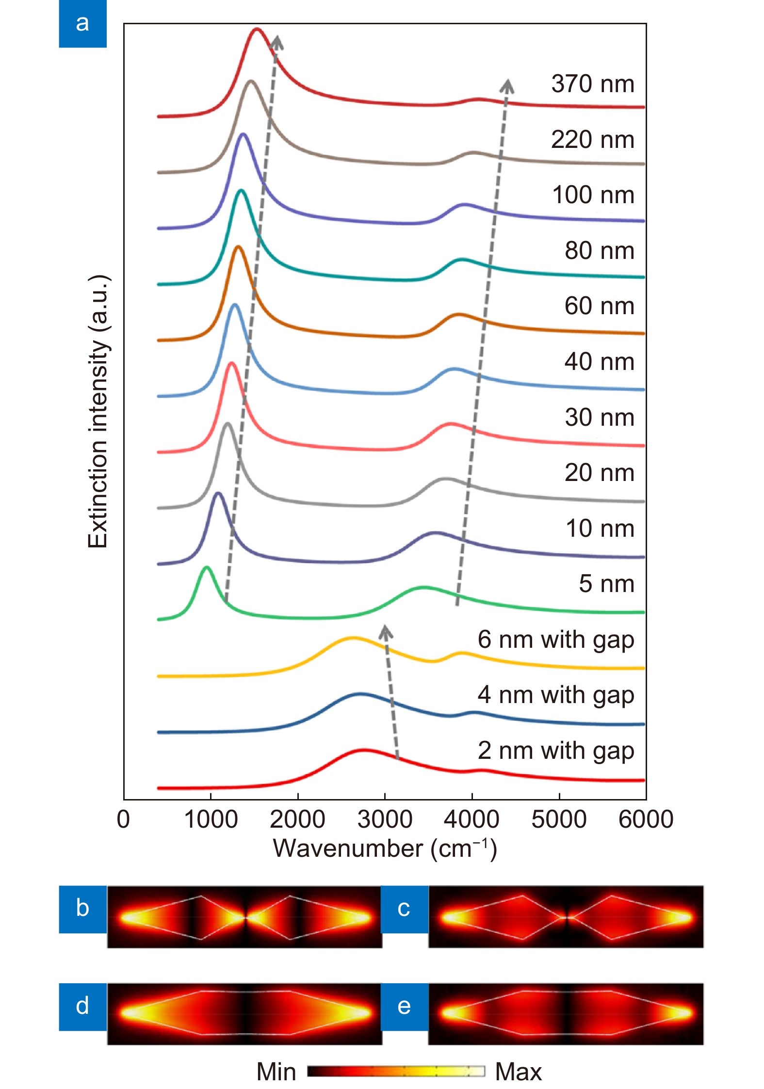
Fig. 3. (a ) Simulated extinction spectra of NBRA structure with different nanobridge width. (b –c ) Simulated mapping of |E z| of bonding dipolar plasmonic band (b) and bonding quadrupolar plasmonic band (c) of a single NBRA structure with a broken nanobridge and 4 nm gap size. (d –e ) Simulated mapping of |E z| at CTP band (d) and BDP band (e) with 370 nm nanobridge width.
An circuit model consisting of resistances (R), inductances (L) and capacitors (C) was built to understand the role of the nanobridge width-tuned plasmonic resonant frequencies and extinction intensities. As shown in the inset of Fig. 4(a), each rhombic arm as well as the nanobridge was modelled as a parallel RLC circuit, and all of three circuits were further connected in series. The total impedance of the circuits system is:
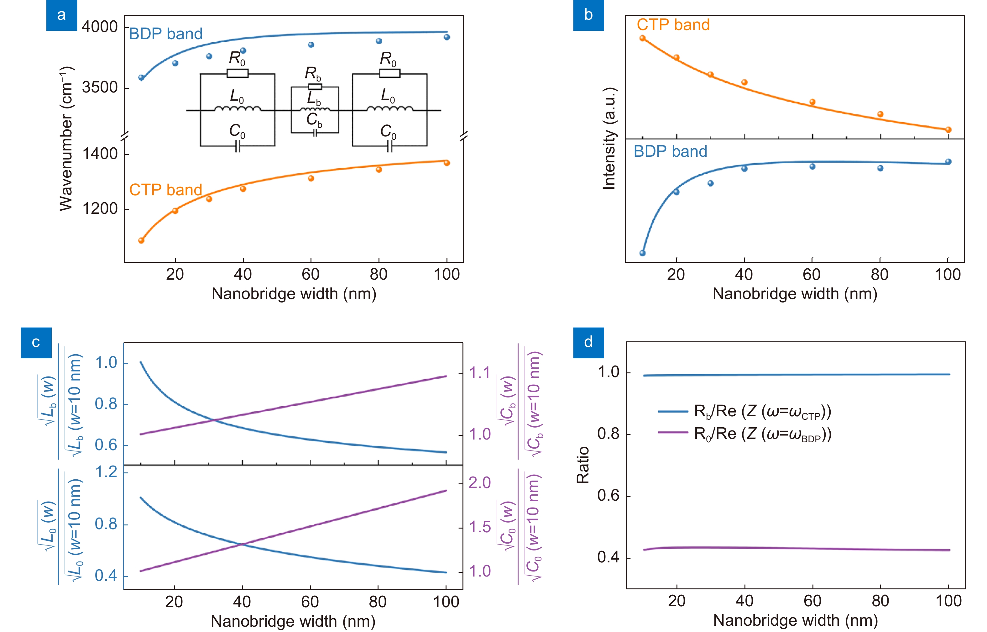
Fig. 4. Nanobridge width-dependent (a ) resonant frequencies and (b ) intensities of CTP and BDP bands. The orange and blue circles are extracted from the simulated extinction spectra (Fig. 3(a)), while the points on the fitting curves are extracted from the spectra of
(Fig. S12, Supplementary information). Inset in (a): RLC circuit model of the NBRA structure. (c ) Nanobridge width-dependent ratio of
(blue curve in the top panel),
(purple curve in the top panel),
(blue curve in the bottom panel) and
(purple curve in the bottom panel). (d) Nanobridge width-dependent ratio of
(blue curve) and
(purple curve).
and
are the deterministic parameters for
.
The extinction spectrum is proportional to the real part of
where
Herein,
In this study, we considered the essential impact of
The detailed derivations of
Fitting
Table 1. Fitting parameters used in the RCL circuit model
|
The analytical form of
However, the exact solutions to Eq. (5) are too complicated to be further analyzed. Instead, we adopted commonly used simplification, independently making the first term or the second term of Eq. (5) be zero. Then we got the simplified solutions:
It can be found that,
The inductances
To study the key quantities to determine the extinction intensities (Fig. 4(b)) of both bands (
Figure 4(d) shows that
3.2 Tunability of MIR resonance and SEIRA
The resonant wavelengths of the two bands can be tuned not only by varying the width of nanobridge, but also by varying the total length

Fig. 5. (a ) Experimental transmittance spectra (normalized) as a function of the length of the NBRAs. (b ) SEIRA spectra of PNTP on NBRAs with total lengths 2.22, 2.40, 2.57 and 2.90 μm in the range of the CTP band.
3.3 Nanogaped NBRA dimer
The spatially superimposed hotspots at the two extremities of the NBRA structure pave the way for further boosting up the local field for both bands in a NBRA dimer with a nanometer-size gap (nanogap). The NBRA dimer was fabricated with a ~20 nm gap size (see the SEM image and AFM topography in Fig. 6(a), 6(c) and
Fig. S3(b), Supplementary information)). Other geometric parameters are the same as those of the structure in Fig. 1. The periodicities of the array are 6400 nm and 1000 nm along the long and short axes of the NBRA dimer, respectively. The normalized experimental transmittance spectra of NBRA dimers also exhibit two pronounced resonance bands in MIR spectral range, one band centered at 1272 cm–1 and the other one centered at 3367 cm–1 (Fig. 6(b)). Both bands of NBRA dimer only redshift less than 100 cm–1 in comparison with the monomer counterparts (Fig. 6(b)). To assign the plasmonic modes associated with the two bands, we employed the s-SNOM to measure the NBRA dimer for both bands. The near-field amplitude and phase images at 1100 cm–1, as shown in Fig. 6(d) and 6(f), as well as the simulated |

Fig. 6. (a ) SEM image of NBRA dimer. (b ) Experimental transmittance of a NBRA and its dimer with gap size 20 nm. (c ) AFM topography of a NBRA dimer. The scale bars in (a) and (c) are 1 μm. Measured near-field amplitude (d ) and phase (f ) of NBRA dimer at 1100 cm−1. Simulated mapping of |E h ) and φ z (j ) of NBRA dimer at 1100 cm−1. Measured near-field amplitude (e ) and phase (g ) of NBRA dimer at 2100 cm−1. Simulated mapping of |E i ) and φ z (k ) of NBRA dimer at 2100 cm−1.
3.4 NBRA dimer-waveguide-cavity coupling
To further enhance LFEFs for both bands, we adopted a strategy by the optical coupling between a localized surface plasmon (LSP) mode and a waveguide-cavity mode14, 65-67. As shown in Fig. 7(a), a NBRA dimer was fabricated on a reflective substrate (the NBRA dimer-on-reflector structure). The reflective substrate was prepared by depositing 3 nm of Ti and 200 nm of Au onto a Si wafer using electron beam evaporation followed by depositing 3 nm of Al and 1400 nm of SiO2 using vacuum magnetron sputtering. Previous studies focused on a single LSP mode coupled with the waveguide cavity mode14, 67. In this study, we are targeting at both gap-coupled CTP and BDP bands rather than only one band of the NBRA that can be simultaneously and constructively coupled with the respective waveguide cavity modes on the same reflective substrate.
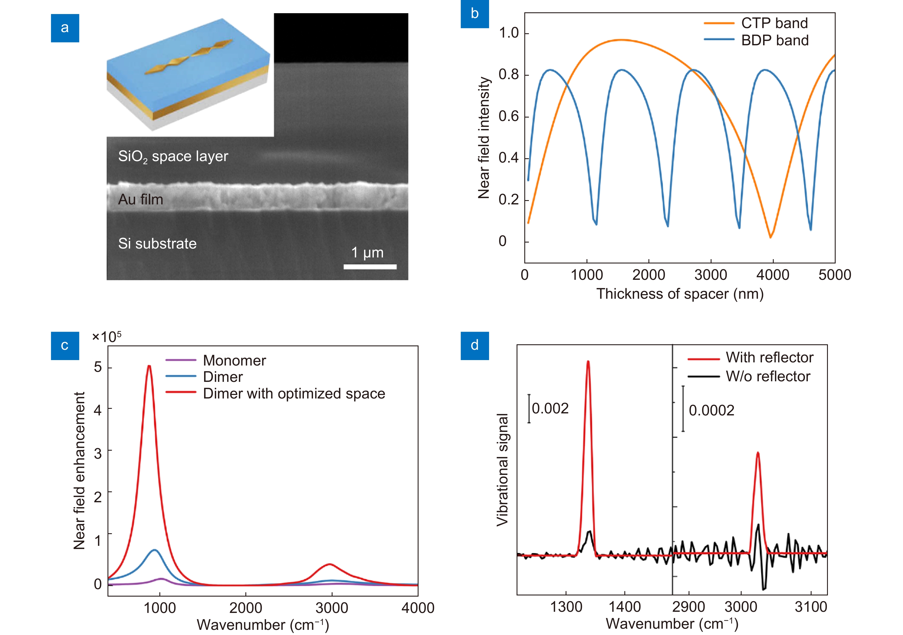
Fig. 7. (a ) SEM of the cross section of the reflective substrate. A 200 nm gold film is sandwiched between a 1400 nm SiO2 spacer layer and the Si substrate. The scale bar is 1 μm. Inset: schematic of the NBRA dimer-on-reflector structure to integrate the waveguide-cavity coupling and nanogap coupling. (b ) Normalized LFEFs of CTP mode (blue curve) and BDP mode (orange curve) as a function of the thickness of the spacer layer. (c ) Simulated LFEFs of monomer, dimer and dimer with 1400 nm SiO2 spacer layer. (d ) SEIRA spectra of PNTP on NBRA dimer on transmitted substrate or on reflective substrate.
We numerically optimized the thickness of the spacer layer to simultaneously maximize the LFEFs in the nanogap of the NBRA dimer for both bands. Figure 7(b) shows that the simulated normalized LFEFs in the nanogap of the NBRA dimer-on-reflector structure for the gap-coupled CTP and BDP bands fluctuate periodically as the thickness of spacer layer (SiO2) increases, with periodicities 4800 nm and 1150 nm, respectively. The periodical behavior can be also predicted through the basic principles for electromagnetic waves68. We found that 1400 nm was the thinnest thickness of the SiO2 layer for almost simultaneously maximizing LFEFs in the nanogap of the NBRA dimer-on-reflector structure with additional 6.6 times and 4.0 times for the gap-coupled CTP and BDP bands, respectively (Fig. 7(c)), in comparison with those of the NBRA dimer without the reflector. Integrally, the LFEFs in the nanogap of the NBRA dimer-on-reflector structure of both bands will be enhanced by 36.75 times and 12.35 times for CTP and BDP bands, respectively, compared with the NBRA monomer through nanogap coupling and waveguide-cavity coupling (Fig. 7(c)).
Experimentally, the SEIRA spectra of a monolayer of PNTP molecules on the surface of the NBRA dimer with or without the reflector structure (thickness of SiO2 spacer layer, 1400 nm) further demonstrate the additional enhancement for both bands through waveguide-cavity coupling (Fig. 7(d)). The integral absorption intensities around 1335 cm–1 and 3024 cm–1 bands for the NBRA dimer-on-reflector structure are 7.4 times and 6.9 times larger than those of NBRA dimer without the reflector. The experimental results show that it is a practical strategy to boost the LFEFs associated with both bands by the waveguide-cavity coupling.
4 Conclusions
In summary, we have reported a nanobridged rhombic structure as a new type of MIRA, effectively exciting the high-order mode (BDP mode) and the fundamental mode (CTP mode) through charge transfer plasmon, which has been demonstrated by the s-SNOM measurements. The RLC circuit analysis reveals that the nanobridge and the linked rhombic-arm antennas mainly act as the inductance and resistance of the overall structure and determines the resonant frequency and intensity of the high-order mode, as well as those of the fundamental band. The hotspots associated with both bands are spatially superimposed, enabling further boosting up the LFEFs of both bands in a NBRA dimer with a nanogap. Integrating waveguide-cavity coupling, the LFEFs in the nanogap of NBRA dimer-on-reflector structure associated with both bands can be simultaneously improved by up to one order of magnitude in contrast to the NBRA monomer counterpart, thereby achieving monolayer sensitivity for two fingerprints.
We provide a new approach for designing multiband antenna by charge transfer plasmon, efficiently exciting the high-order modes, along with elaborating the importance of the nanobridge and nanogap in MIRAs. These findings also indicate that the island-like metallic films developed as the SEIRA-active substrates in the early stage of SEIRA in 1980s could be considered as nanogap-coupled MIRAs with nanobridges69. We believe that designing novel structures with nanobridges accompanied with nanogaps can be a promising strategy for producing multiband MIRAs for general applications in SEIRA, heat-management, and ultrasensitive MIR detectors in the future.
[1] . Surface-enhanced infrared spectroscopy. Appl Spectrosc, 2004, 58: 324A-338A.
[2] . Tailoring plasmonic substrates for surface enhanced spectroscopies. Chem Soc Rev, 2008, 37: 898-911.
[4] . Surface-enhanced infrared spectroscopy using resonant nanoantennas. Chem Rev, 2017, 117: 5110-5145.
[5] . Nanomaterial-based plasmon-enhanced infrared spectroscopy. Adv Mater, 2018, 30: 1704896.
[6] . Metasurface-based molecular biosensing aided by artificial intelligence. Angew Chem Int Ed, 2019, 58: 14810-14822.
[7] . Semiconductor infrared plasmonics. Nanophotonics, 2019, 8: 949-990.
[8] . Low-loss, infrared and terahertz nanophotonics using surface phonon polaritons. Nanophotonics, 2015, 4: 44-68.
[9] . Phonon-polaritonic bowtie nanoantennas: controlling infrared thermal radiation at the nanoscale. ACS Photonics, 2017, 4: 1753-1760.
[10] . Nanoimaging of resonating hyperbolic polaritons in linear boron nitride antennas. Nat Commun, 2017, 8: 15624.
[11] . Boron nitride nanoresonators for phonon-enhanced molecular vibrational spectroscopy at the strong coupling limit. Light Sci Appl, 2018, 7: 17172.
[12] . History, current developments, and future directions of near-field optical science. Opto-Electron Adv, 2020, 3: 190046.
[13] . Antennas for light. Nat Photonics, 2011, 5: 83-90.
[14] . Nanogapped Au antennas for ultrasensitive surface-enhanced infrared absorption spectroscopy. Nano Lett, 2017, 17: 5768-5774.
[15] . Coupled-mode theory for plasmonic resonators integrated with silicon waveguides towards mid-infrared spectroscopic sensing. Opt Express, 2020, 28: 2020-2036.
[16] . Autonomic molecular transport for ultrasensitive surface-enhanced infrared absorption spectroscopy. ACS Appl Polym Mater, 2020, 2: 3929-3935.
[17] . Ultrasensitive skin-like wearable optical sensors based on glass micro/nanofibers. Opto-Electron Adv, 2020, 3: 190022.
[18] . On-chip readout plasmonic mid-IR gas sensor. Opto-Electron Adv, 2020, 3: 190040.
[19] . Beam engineering of quantum cascade lasers. Laser Photonics Rev, 2012, 6: 24-46.
[20] . Surface plasmon enhanced infrared photodetection. Opto-Electron Adv, 2019, 2: 180026.
[21] . High-responsivity mid-infrared graphene detectors with antenna-enhanced photocarrier generation and collection. Nano Lett, 2014, 14: 3749-3754.
[22] . Advances of surface-enhanced Raman and IR spectroscopies: from nano/microstructures to macro-optical design. Light Sci Appl, 2021, 10: 161.
[23] . Effective wavelength scaling for optical antennas. Phys Rev Lett, 2007, 98: 266802.
[24] . Resonant plasmonic and vibrational coupling in a tailored nanoantenna for infrared detection. Phys Rev Lett, 2008, 101: 157403.
[25] . Ultra-sensitive vibrational spectroscopy of protein monolayers with plasmonic nanoantenna arrays. Proc Natl Acad Sci USA, 2009, 106: 19227-19232.
[26] . Surface-enhanced infrared absorption using individual cross antennas tailored to chemical moieties. J Am Chem Soc, 2013, 135: 3688-3695.
[27] . Vibrational near-field mapping of planar and buried three-dimensional plasmonic nanostructures. Nat Commun, 2013, 4: 2237.
[28] . Surface-enhanced infrared spectroscopy using nanometer-sized gaps. ACS Nano, 2014, 8: 4908-4914.
[29] . Revealing the plasmon coupling in gold nanochains directly from the near field. Opto-Electron Adv, 2019, 2: 180030.
[30] . Resonances of individual lithographic gold nanowires in the infrared. Appl Phys Lett, 2008, 93: 163105.
[32] . On chip plasmonic monopole nano-antennas and circuits. Nano Lett, 2011, 11: 5219-5226.
[33] . Dual-band perfect absorber for multispectral plasmon-enhanced infrared spectroscopy. ACS Nano, 2012, 6: 7998-8006.
[34] . Multi-resonant metamaterials based on UT-shaped nano-aperture antennas. Opt Express, 2011, 19: 7921-7928.
[35] . Multi-resonant compact nanoaperture with accessible large nearfields. Appl Phys B, 2015, 118: 29-38.
[36] . Fractal diabolo antenna for enhancing and confining the optical magnetic field. AIP Adv, 2014, 4: 017123.
[37] . Fractal nanoparticle plasmonics: the cayley tree. ACS Nano, 2015, 9: 3284-3292.
[38] . Multispectral cesaro-type fractal plasmonic nanoantennas. ACS Photonics, 2016, 3: 2102-2111.
[39] . Ultrasensitive broadband probing of molecular vibrational modes with multifrequency optical antennas. ACS Nano, 2013, 7: 669-675.
[40] . Planar wallpaper group metamaterials for novel terahertz applications. Opt Express, 2008, 16: 18565-18575.
[41] . Conformal dual-band near-perfectly absorbing mid-infrared metamaterial coating. ACS Nano, 2011, 5: 4641-4647.
[42] . Resolving molecule-specific information in dynamic lipid membrane processes with multi-resonant infrared metasurfaces. Nat Commun, 2018, 9: 2160.
[43] . Near-field imaging of optical antenna modes in the mid-infrared. Opt Express, 2008, 16: 20295-20305.
[44] . Optical near-field mapping of plasmonic nanoprisms. Nano Lett, 2008, 8: 3357-3363.
[45] . Controlling the near-field oscillations of loaded plasmonic nanoantennas. Nat Photonics, 2009, 3: 287-291.
[46] . Resolving the electromagnetic mechanism of surface-enhanced light scattering at single hot spots. Nat Commun, 2012, 3: 684.
[47] . Visualizing the near-field coupling and interference of bonding and anti-bonding modes in infrared dimer nanoantennas. Opt Express, 2013, 21: 1270-1280.
[48] . Optical dielectric function of gold. Phys Rev B, 2012, 86: 235147.
[49] . “Sketch and peel” lithography for high-resolution multiscale patterning. Nano Lett, 2016, 16: 3253-3259.
[50] . Rapid focused ion beam milling based fabrication of plasmonic nanoparticles and assemblies
[51] . Topology optimization-based inverse design of plasmonic nanodimer with maximum near-field enhancement. Adv Funct Mater, 2020, 30: 2000642.
[52] . Reliable patterning, transfer printing and post-assembly of multiscale adhesion-free metallic structures for nanogap device applications. Adv Funct Mater, 2020, 30: 2002549.
[53] . Sub-10 nm fabrication: methods and applications. Int J Extrem Manuf, 2021, 3: 032002.
[54] . A perfect smoother. Anal Chem, 2003, 75: 3631-3636.
[55] . Pseudoheterodyne detection for background-free near-field spectroscopy. Appl Phys Lett, 2006, 89: 101124.
[56] . Nanoplasmonics: classical down to the nanometer scale. Nano Lett, 2012, 12: 1683-1689.
[57] . Surface-enhanced infrared absorption spectroscopy using charge transfer plasmons. ACS Photonics, 2019, 6: 1272-1278.
[58] . Charge transfer plasmons: optical frequency conductances and tunable infrared resonances. ACS Nano, 2015, 9: 6428-6435.
[59] . A circuit model for plasmonic resonators. Opt Express, 2014, 22: 9809-9819.
[60] . Study of plasmon resonance in a gold nanorod with an LC circuit model. Opt Express, 2009, 17: 6407-6413.
[61] . Scaling of losses with size and wavelength in nanoplasmonics and metamaterials. Appl Phys Lett, 2011, 99: 211106.
[62] . Saturation of the magnetic response of split-ring resonators at optical frequencies. Phys Rev Lett, 2005, 95: 223902.
[63] . Fano resonances in nanoscale plasmonic systems: a parameter-free modeling approach. Nano Lett, 2011, 11: 2835-2840.
[64] . Mapping the near fields of plasmonic nanoantennas by scattering-type scanning near-field optical microscopy. Laser Photonics Rev, 2015, 9: 637-649.
[65] . Single molecule directivity enhanced raman scattering using nanoantennas. Nano Lett, 2012, 12: 2625-2630.
[66] . Directional raman scattering from single molecules in the feed gaps of optical antennas. Nano Lett, 2013, 13: 2194-2198.
[67] . Fan-shaped gold nanoantennas above reflective substrates for surface-enhanced infrared absorption (SEIRA). Nano Lett, 2015, 15: 1272-1280.
[69] . Dynamic processes in electrochemical reactions studied by surface-enhanced infrared absorption spectroscopy (SEIRAS). Bull Chem Soc Jpn, 1997, 70: 2861-2880.
Article Outline
En-Ming You, Yiqin Chen, Jun Yi, Zhao-Dong Meng, Qian Chen, Song-Yuan Ding, Huigao Duan, Martin Moskovits, Zhong-Qun Tian. Nanobridged rhombic antennas supporting both dipolar and high-order plasmonic modes with spatially superimposed hotspots in the mid-infrared[J]. Opto-Electronic Advances, 2021, 4(12): 210076-1.
