Journal of Semiconductors, 2024, 45 (1): 012503, Published Online: Mar. 13, 2024  

Electrical properties and structural optimization of GaN/InGaN/GaN tunnel junctions grown by molecular beam epitaxy

Author Affiliations
1 School of Nano-Tech and Nano-Bionics, University of Science and Technology of China, Hefei 230026, China
2 Suzhou Institute of Nano-Tech and Nano-Bionics, Chinese Academy of Sciences, Suzhou 215123, China
Abstract
The InGaN films and GaN/InGaN/GaN tunnel junctions (TJs) were grown on GaN templates with plasma-assisted molecular beam epitaxy. As the In content increases, the quality of InGaN films grown on GaN templates decreases and the surface roughness of the samples increases. V-pits and trench defects were not found in the AFM images. p++-GaN/InGaN/n++-GaN TJs were investigated for various In content, InGaN thicknesses and doping concentration in the InGaN insert layer. The InGaN insert layer can promote good interband tunneling in GaN/InGaN/GaN TJ and significantly reduce operating voltage when doping is sufficiently high. The current density increases with increasing In content for the 3 nm InGaN insert layer, which is achieved by reducing the depletion zone width and the height of the potential barrier. At a forward current density of 500 A/cm2, the measured voltage was 4.31 V and the differential resistance was measured to be 3.75 × 10?3 Ω·cm2 for the device with a 3 nm p++-In0.35Ga0.65N insert layer. When the thickness of the In0.35Ga0.65N layer is closer to the “balanced” thickness, the TJ current density is higher. If the thickness is too high or too low, the width of the depletion zone will increase and the current density will decrease. The undoped InGaN layer has a better performance than n-type doping in the TJ. Polarization-engineered tunnel junctions can enhance the functionality and performance of electronic and optoelectronic devices.

1. Introduction

Tunnel junctions (TJs) provide a promising method for the hole injection of p-type GaN. Several research groups have reported preliminary studies of TJs[15]. In reverse biased TJs, electrons in the valence band of p-type materials tunnel into the conduction band of n-type materials. Efficient tunneling junctions in Ⅲ-nitride devices can help achieve new device structures and also enhance the performance of electronic and optoelectronic devices[610]. However, the low efficiency of the interband tunneling process hinders the widespread application of TJs in electronic and optoelectronic devices. Polarization engineering can overcome the inherent obstacles of these materials. This is done by using the interfacial polarization of the GaN/AlGaN/GaN[11, 12] or GaN/InGaN/GaN[6, 13, 14] junction to induce the high electric field so that the valence band and conduction band on both sides of the junction are aligned. When the InGaN barrier with a lower band gap is used, the decrease of the depletion width and the decrease of the energy barrier results in the high reverse current density[15] of the GaN-based tunnel junction and the tunneling characteristics of the negative differential resistance[16, 17].

Efforts are also being made to develop tunnel junctions grown by metal–organic chemical vapor deposition (MOCVD)[10, 18, 19], and low-resistance TJ has been achieved using InGaN layers with high In content (40%)[20]. However, the use of an InGaN insert layer with a higher component will lead to the deterioration of material quality, strain management and other problems. The use of the high-component InGaN insert layer in TJs remains the main challenge in MOCVD growth. Mg activation is required, which is a big challenge for tunnel junctions grown by MOCVD. The top of a typical tunnel junction used in optoelectronic devices is covered by an n-type layer. It has been reported that hydrogen can only pass through the p-type layer, but not the n-type layer[21, 22]. It requires very complex technological means to activate Mg by mesas etching and thermal annealing[18].

In this work, the InGaN films and GaN/InGaN/GaN TJs were grown on GaN templates by plasma-assisted molecular beam epitaxy (MBE). There is no memory effect of Mg grown by MBE and annealing process after growth is not required since Mg is not passivated by hydrogen. We characterized the properties of InGaN films and we have systematically investigated the effect of the InGaN insert layer in TJs on device electrical properties, in which the InGaN insert layers was various in In composition, InGaN thicknesses and doping concentration. Our results show that GaN/InGaN/GaN TJs can promote good interband tunneling and significantly reduce operating voltage when doping sufficiently large. These low-resistance TJs can be applied to high-power LEDs and laser diodes.

2. Experiment

The samples in this article were grown with the GEN-20A MBE system. The GEN-20A MBE system is a plasma-assisted MBE using a plasma nitrogen source. Other sources such as In, Ga, Mg, and Si are all elemental sources. The N2 flux and radio-frequency plasma power used during the growth were 1.5 sccm and 330 W, respectively. We first grew three single-layer InGaN samples with different In contents on the GaN templates, named S1, S2, and S3 according to the In content from low to high. After determining the single-layer InGaN, we prepared a device containing GaN/InGaN/GaN tunnel junctions, and all structural parameters are shown in Fig. 1. The schematic diagram of the device structure is shown in Fig. 1(a). The epitaxial layers were grown on GaN templates. Firstly, there is a PIN structure, including a 2 μm n-GaN layer, a 20 nm undoped GaN layer, and a 120 nm p-GaN layer. Then there is a p++-GaN/InGaN/n++-GaN TJ layer. The thickness of the p++-GaN layer is 20 nm, and the Mg doping concentration is 1.2 × 1020 cm−3. The thickness of the n++-GaN layer is 10 nm, and the Si doping concentration is 1.5 × 1020 cm−3. The In content of the InGaN insert layer was designed to be 10%, 25%, and 35%. The thickness of InGaN layer was designed as 3 nm and 5 nm. The doping type at the InGaN insertion layer also varied. Last, a 200 nm thick n-GaN contact layer (Si: 1 × 1019 cm−3) was grown. The specific structural parameters of GaN/InGaN/GaN TJs are listed in Table 1. After the epitaxial growth was completed, in order to conduct Ⅳ testing, n-type metal electrodes were deposited at both the upper and lower n-GaN layers. The n-type GaN layers were grown at 760 °C (Si: 1 × 1019 cm−3) and 680 °C (Si: 1.5 × 1020 cm−3, the layer at the TJ). The p-type GaN layers were grown at 760 °C (Mg: 2 × 1019 cm−3 and Mg: 1.2 × 1020 cm−3). The InGaN layers were grown at 680, 630, and 600 °C, and the corresponding In contents were 10%, 25% and 35%, respectively. The temperature was measured by the thermocouple, and the wafer temperature is about 90% of the temperature of the thermocouple. Fig. 1(b) shows the equivalent circuit diagram of the device. The resistance in the entire circuit can be divided into three parts, including contact resistance, bulk resistance, and tunnel junction resistance. Among them, the contact resistance includes the n-GaN ohmic contact resistance Rc1 on the top surface and the n-GaN ohmic contact resistance Rc2 on the lower mesa. Bulk resistance include upper n-type bulk GaN resistance Rn1, p-type bulk GaN resistance Rp, lower n-type bulk GaN vertical resistance Rn2, and lower n-type bulk GaN lateral resistance Rn3. Junction resistance includes tunnel junction resistance RTJ and pn junction resistance.
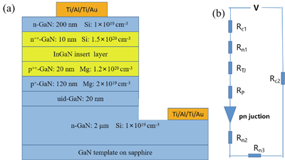
Fig. 1. (Color online) (a) Schematic diagram of the device structure including GaN/InGaN/GaN TJ. (b) Equivalent circuit diagram of the device.

下载图片 查看所有图片

Table 1. The specific structural parameters of GaN/InGaN/GaN TJ.

p++-GaN: 20 nm (1020 cm−3)Insert layer InGaNn++-GaN: 10 nm (1020 cm−3)
Sample AMg: 1p++-In0.1Ga0.9N: 3 nmMg: 1 × 1020 cm−3Si: 0.5
Sample BMg: 1.2p++-In0.1Ga0.9N: 3 nmMg: 6 × 1020 cm−3Si: 1.5
Sample CMg: 1.2 p++-In0.25Ga0.75N: 3 nmMg: 6 × 1020 cm−3Si: 1.5
Sample DMg: 1.2p++-In0.35Ga0.65N: 3 nmMg: 6 × 1020 cm−3Si: 1.5
Sample EMg: 1.2No InGaN insert layerMg: 6 × 1020 cm−3Si: 1.5
Sample FMg: 1.2 Uid-In0.35Ga0.65N: 3 nmSi: 1.5
Sample GMg: 1.2 Uid-In0.35Ga0.65N: 5 nmSi: 1.5
Sample HMg: 1.2 n-In0.35Ga0.65N: 3 nmSi: 2 × 1019 cm−3Si: 1.5

查看所有表

The samples were processed by lithography techniques. Firstly, photoetching a window is required by etching. Secondly, etching mesa by ion beam etching equipment. Thirdly, photoetching metal windows on the mesa and under the mesa. Lastly, depositing metal, wherein the contact metal on the mesa and under the mesa is n-type ohmic contact, and the metal of each layer is classified as Ti/Al/Ti/Au. The In content of the InGaN layers was calibrated by X-ray diffraction (XRD). The surface morphology of the InGaN layers was characterized by atomic force microscope (AFM). The doping concentrations of Mg and Si were calibrated by secondary ion mass spectroscopy (SIMS) on separate doping calibration growth stacks. The interface at the tunnel junction was characterized by high-resolution transmission electron microscopy (HRTEM).

3. Results and discussion

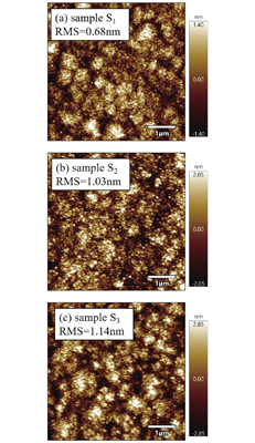
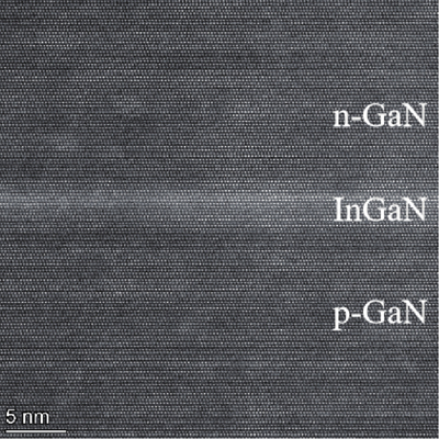
As mentioned earlier, we grew three bulk layer InGaN films on GaN templates, named S1, S2, and S3 according to the In content from low to high. The XRD ω−2θ patterns of the three samples are shown in Figs. 2(a)−2(c). Due to the InGaN layer thickness of 300 nm, assuming that the three films are completely relaxed, according to XRD fitting results, the In contents of the three are 10%, 25%, and 35%, respectively. The surface AFM images of the three samples are shown in Figs. 3(a)–3(c). The surface morphology of samples S1, S2, and S3 are all three-dimensional island morphology. The surface roughness of the three samples are 0.68, 1.03 and 1.14 nm, respectively. With the increase of In content in the sample, the surface undulation becomes larger and the roughness increases. The morphology of high In content InGaN reported by other groups is also the same[2325]. When the migration distance of atoms is less than the width of the terrace, atoms far away from the terrace will not be able to migrate to and incorporate into the step edge, but will directly nucleate on the terrace, resulting in a three-dimensional island growth mode. In addition, V-pits[26] and trench defects[27] were not found. The HRTEM image of the tunnel junction is shown in Fig. 4. The tunnel junction interface is relatively flat, and the thickness of the InGaN layer is about 2.6 nm, which is about the same as our designed thickness of 3 nm.
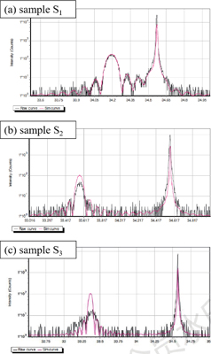
Fig. 2. (Color online) XRD ω−2θ patterns of the three samples (a) S1 , (b) S2 , (c) S3. The black curve represents the experimental curve, while the red curve represents the simulation curve.

下载图片 查看所有图片

Fig. 3. (Color online) Surface AFM images of the three samples (a) S1, (b) S2, (c) S3.

下载图片 查看所有图片

Fig. 4. HRTEM image of the tunnel junction.

下载图片 查看所有图片

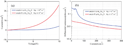
To study the effect of Mg and Si doping concentrations in TJs on device IV characteristics, we prepared samples A and B. The doping concentration of p++-GaN/p++-InGaN/n++-GaN in sample A is 1 × 1020 cm−3, 1 × 1020 cm−3, and 5 × 1019 cm−3 respectively, and the corresponding doping concentration in sample B is 1.2 × 1020 cm−3, 6 × 1020 cm−3, and 1.5 × 1020 cm−3, respectively. The IV curves of the samples are shown in Fig. 5(a). Through circular transmission line testing, it was confirmed that the top n-type contact is an ohmic contact. At a current density of 200 A/cm2, the measured voltages of samples A and B were 8.49 and 3.40 V, respectively. As the forward current density reached 500 A/cm2, the voltage of sample A exceeded 10 V, the sample B showed forward voltage of 5.51 V. The InGaN insert layer can promote good interband tunneling in the GaN/InGaN/GaN TJ and significantly reduce operating voltage when doping is sufficiently high. This can be explained by the following reasons. Firstly, with the increase of Mg and Si doping concentration, the built-in electric field in the TJ is enhanced, as a result the barrier width is reduced, and thus the tunneling probability is increased. Second, owing to higher doping concentrations, more electrons and holes in a certain energy level satisfies the tunneling condition, and then result in a larger tunneling current. Third, deep level defects will be generated under heavily doped materials, which will form auxiliary tunneling levels and reduce the barrier required for tunneling. The equivalent band diagram of a GaN/InGaN/GaN TJ can be referenced in literature[28].

Fig. 5. (Color online) (a) IV curves of the samples, the doping concentration at the TJ of the samples varies, and (b) the change of differential resistance at forward current density.

下载图片 查看所有图片

The change of differential resistance at forward current density is shown in Fig. 5(b). Sample A and sample B had different differential resistance changes. Sample A exhibited high resistance at very low current density (less than 30 A/cm2), and the differential resistance dropped sharply when the sample was turned on. Sample B showed a decrease in differential resistance with increasing forward voltage. Compared with sample A, sample B showed a lower operating voltage and lower differential resistance, which is attributed to higher Si and Mg doping concentrations in TJs.

To study the effect of In content in the InGaN insert layer on device IV characteristics, we prepared sample B, C, D and E. The In content of the InGaN insert layer was designed to be 10% (sample B), 25% (sample C), 35% (sample D), and 0% (sample E, no InGaN layer). The IV curves of the four samples are shown in Fig. 6(a). At a current density of 500 A/cm2, the measured voltages of samples B, C, D, and E were 5.64, 5.21, 4.31, and 6.02 V, respectively. As the current density reached 2000 A/cm2, the devices showed voltages of 9.29, 8.28, 7.57, and 9.47 V, respectively. These results show that the operating voltage of sample D (3 nm In0.35Ga0.65N) is much lower compared to sample E (no InGaN). The change of differential resistance at the forward current density is shown in Fig. 6(b). The change in differential resistance of the four samples is very similar, and the differential resistance decreases with increasing forward voltage. At a current density of 500 A/cm2, the differential resistances were measured to be 4.82 × 10⁻³, 3.72 × 10⁻³, 3.75 × 10⁻³, and 4.52 × 10⁻³ Ω·cm2 for samples B, C, D and E respectively. Samples C and D showed lower voltage and lower differential resistance across all current ranges compared to samples B and E. With the increase of In content in the InGaN insert layer, the band gap of InGaN becomes narrower and the tunneling barrier height becomes lower. On the other hand, the polarization field also increases with the increase of In content, and the tunneling barrier width becomes narrower. Therefore, the current density at the same forward bias voltage increases.
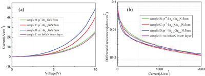
Fig. 6. (Color online) (a) IV curves of the samples, In content of the InGaN layer at the tunnel junction changes, (b) the change of differential resistance at forward current density.

下载图片 查看所有图片

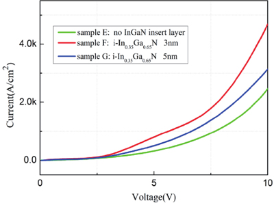
To study the effect of thickness of In0.35Ga0.65N insert layer in TJ on device IV characteristics, we prepared sample E, sample F and sample G. The thickness of the In0.35Ga0.65N insert layer was 0 (sample E, no InGaN layer), 3 (sample F), and 5 nm (sample G). The IV curves of the samples are shown in Fig. 7. At a forward current density of 1000 A/cm2, the measured voltages of samples E, F and G were 7.68, 5.61 and 6.65 V, respectively. Under the same bias voltage, the current density of sample E was the smallest, the current density of sample F was the largest, and the current density of sample G was between the two. When the polarization electric field generated by the InGaN interlayer aligns the valence band of p-type GaN with the conduction band of n-type GaN, implying that they are in the same quantum state[7], and the thickness of InGaN is called as the “balanced” thickness. For InGaN with an In content of 0.35, the “balanced” thickness is estimated to be 3 nm[28]. When the thickness of InGaN (sample E: InGaN 0 nm) is less than the “balanced” thickness (sample F: InGaN 3 nm), the width of depletion region near the interface of n-type GaN and p-type GaN increases, that is, the width of the barrier increases. When the thickness of InGaN (sample G: InGaN 5 nm) is greater than the “balanced” thickness (sample F: InGaN 3 nm), the width of the InGaN barrier layer increases. The tunneling barrier mainly comes from the InGaN interlayer. In n-type GaN and p-type GaN, although the width of the carrier depletion region decreases, the increase of the barrier width in the middle InGaN layer is larger than the decrease of the barrier width in both sides, so the total tunnel probability decreases and the tunneling current density decreases.

Fig. 7. (Color online) IV curves of the samples, thickness of InGaN layer at tunnel junction varies.

下载图片 查看所有图片

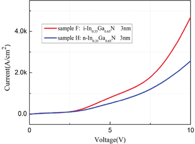
To study the effect of doping in the In0.35Ga0.65N insert layer on device IV characteristics, we prepared sample F and sample H. The InGaN layer in sample F was not doped, and the InGaN layer in sample H was doped with Si with a concentration of 2 × 1019 cm−3. The IV curves of the samples are shown in Fig. 8. At a forward current density of 1000 A/cm2, the measured voltages for sample F and sample H were 5.61 and 6.91 V, respectively. In the whole range, the current density of sample F is higher than that of sample H under the same forward bias voltage. Since the actual doping curve is not exactly the same as the ideal, the doping curve would be trailing. If Si doping is present in the InGaN insert layer (compared to no Si doping), a portion of Si will be incorporated into the p-type GaN layer[29], reducing the hole concentration in the p-type GaN layer and increasing the tunneling distance. This doping profile may be the primary cause of the higher operating voltage. We can confirm this conjecture through SIMS testing. The distribution of acceptors (Mg) and donors (Si) at the interface of the tunnel junction has a great influence on the resistivity of the tunnel junction. Akatsuka found that an overlap between Mg and Si at the tunnel junction interface was effective in helping to obtain a lower resistivity of the GaN tunnel junctions[30]. We may be able to tune the doping profile at the tunnel junction to control the tunnel junction resistivity.

Fig. 8. (Color online) IV curves of the samples, doping in InGaN layers at tunnel junctions changes.

下载图片 查看所有图片

4. Conclusion

In summary, the InGaN films and GaN/InGaN/GaN tunnel junctions (TJs) were grown on GaN templates by plasma-assisted MBE. As the In content increases, the quality of InGaN films grown on GaN templates decreases and the surface roughness of the samples increases. V-pits and trench defects were not found in the AFM images. p++-GaN/InGaN/n++-GaN TJs were investigated for various In content, InGaN thicknesses and doping concentration in the InGaN insert layer. InGaN insert layer can promote good interband tunneling in GaN/InGaN/GaN TJs and significantly reduce operating voltage when doping is sufficiently high. The current density increases with increasing In content for 3 nm InGaN insert layer, which is achieved by reducing the depletion zone width and the height of the potential barrier. At a forward current density of 500 A/cm2, the measured voltage was 4.31 V and the differential resistance was measured to be 3.75 × 10⁻³ Ω·cm2 for the device with the 3 nm p++-In0.35Ga0.65N insert layer. When the thickness of the In0.35Ga0.65N layer is closer to the “balanced” thickness, the TJ current density is higher. If the thickness is too high or too low, the width of the depletion zone will increase and the current density will decrease. The undoped InGaN layer has better performance than n-type doping in TJs. Polarization-engineered tunnel junctions can enhance the functionality and performance of electronic and optoelectronic devices.

5 Acknowledge

This work was supported by the National Key Research and Development Program of China (2017YFE0131500, 2022YFB2802801), the National Natural Science Foundation of China (61834008, U21A20493), the Key Research and Development Program of Jiangsu Province (BE2020004, BE2021008-1), and the Suzhou Key Laboratory of New-type Laser Display Technology (SZS2022007). The authors are grateful for the technical support for Nano-X from the Suzhou Institute of Nano-Tech and Nano-Bionics, Chinese Academy of Sciences (SINANO), Chinese Academy of Sciences.

References

[1] TakeuchiTHasnainGCorzineSet alGaN-based light emitting diodes with tunnel junctionsJpn J Appl Phys200140L86110.1143/JJAP.40.L861

[2] OzdenIMakaronaENurmikkoA Vet alA dual-wavelength indium gallium nitride quantum well light emitting diodeAppl Phys Lett200179253210.1063/1.1410345

[3] SongY KZhouHDiagneMet alA vertical cavity light emitting InGaN quantum well heterostructureAppl Phys Lett199974344110.1063/1.124121

[4] JeonS ROhC SYangJ Wet alGaN tunnel junction as a current aperture in a blue surface-emitting light-emitting diodeAppl Phys Lett200280193310.1063/1.1459487

[5] DiagneMHeYZhouHet alVertical cavity violet light emitting diode incorporating an aluminum gallium nitride distributed Bragg mirror and a tunnel junctionAppl Phys Lett200179372010.1063/1.1415405

[6] KrishnamoorthySAkyolFRajanSInGaN/GaN tunnel junctions for hole injection in GaN light emitting diodesAppl Phys Lett201410514110410.1063/1.4897342

[7] KrishnamoorthySNathD NAkyolFet alPolarization-engineered GaN/InGaN/GaN tunnel diodesAppl Phys Lett20109720350210.1063/1.3517481

[8] ZhangZ HTiam TanSKyawZet alInGaN/GaN light-emitting diode with a polarization tunnel junctionAppl Phys Lett201310219350810.1063/1.4806978

[9] YoungE CYonkeeB PWuFet alHybrid tunnel junction contacts to III–nitride light-emitting diodesAppl Phys Express2016902210210.7567/APEX.9.022102

[10] KagaMMoritaTKuwanoYet alGaInN-based tunnel junctions in n–p–n light emitting diodesJpn J Appl Phys20135208JH0610.7567/JJAP.52.08JH06

[11] YangJZhaoD GLiuZ Set alA 357.9 nm GaN/AlGaN multiple quantum well ultraviolet laser diodeJ Semicond20224301050110.1088/1674-4926/43/1/010501

[12] HeikmanSKellerSWuYet alPolarization effects in AlGaN/GaN and GaN/AlGaN/GaN heterostructuresJ Appl Phys2003931011410.1063/1.1577222

[13] ZhangM LIkedaMHuangS Yet alNi/Pd-based ohmic contacts to p-GaN through p-InGaN/p+-GaN contacting layersJ Semicond20224309280310.1088/1674-4926/43/9/092803

[14] LiW JSharminSIlatikhamenehHet alPolarization-engineered III-nitride heterojunction tunnel field-effect transistorsIEEE J Explor Solid State Comput Devices Circuits201512810.1109/JXCDC.2015.2426433

[15] KrishnamoorthySParkP SRajanSDemonstration of forward inter-band tunneling in GaN by polarization engineeringAppl Phys Lett20119923350410.1063/1.3666862

[16] SimonJZhangZGoodmanKet alPolarization-induced zener tunnel junctions in wide-band-gap heterostructuresPhys Rev Lett200910302680110.1103/PhysRevLett.103.026801

[17] YanX DLiW JIslamS Met alPolarization-induced zener tunnel diodes in GaN/InGaN/GaN heterojunctionsAppl Phys Lett201510716350410.1063/1.4934269

[18] KuwanoYKagaMMoritaTet alLateral hydrogen diffusion at p-GaN layers in nitride-based light emitting diodes with tunnel junctionsJpn J Appl Phys20135208JK1210.7567/JJAP.52.08JK12

[19] AkyolFZhangY WKrishnamoorthySet alUltralow-voltage-drop GaN/InGaN/GaN tunnel junctions with 12% indium contentAppl Phys Express20171012100310.7567/APEX.10.121003

[20] TakasukaDAkatsukaYInoMet alGaInN-based tunnel junctions with graded layersAppl Phys Express2016908100510.7567/APEX.9.081005

[21] PankoveJ IMageeC WWanceR OHole-mediated chemisorption of atomic hydrogen in siliconAppl Phys Lett19854774810.1063/1.96026

[22] NeugebauerJVan de WalleC GRole of hydrogen in doping of GaNAppl Phys Lett199668182910.1063/1.116027

[23] JiangL RLiuJ PTianA Qet alGaN-based green laser diodesJ Semicond20163711100110.1088/1674-4926/37/11/111001

[24] LiangFZhaoD GLiuZ Set alGaN-based blue laser diode with 6.0 W of output power under continuous-wave operation at room temperatureJ Semicond20214211280110.1088/1674-4926/42/11/112801

[25] PristovsekMKadirAMeissnerCet alGrowth mode transition and relaxation of thin InGaN layers on GaN (0001)J Cryst Growth20133726510.1016/j.jcrysgro.2013.03.012

[26] SuihkonenSSvenskOLangTet alThe effect of InGaN/GaN MQW hydrogen treatment and threading dislocation optimization on GaN LED efficiencyJ Cryst Growth200729874010.1016/j.jcrysgro.2006.10.131

[27] MassabuauF C PTrinh-XuanLLodiéDet alCorrelations between the morphology and emission properties of trench defects in InGaN/GaN quantum wellsJ Appl Phys201311307350510.1063/1.4792505

[28] KrishnamoorthySAkyolFParkP Set alLow resistance GaN/InGaN/GaN tunnel junctionsAppl Phys Lett201310211350310.1063/1.4796041

[29] HamdyS WYoungE CAlhassanA Iet alEfficient tunnel junction contacts for high-power semipolar III-nitride edge-emitting laser diodesOpt Express201927832710.1364/OE.27.008327

[30] AkatsukaYIwayamaSTakeuchiTet alDoping profiles in low resistive GaN tunnel junctions grown by metalorganic vapor phase epitaxyAppl Phys Express20191202550210.7567/1882-0786/aafca8

Jun Fang, Fan Zhang, Wenxian Yang, Aiqin Tian, Jianping Liu, Shulong Lu, Hui Yang. Electrical properties and structural optimization of GaN/InGaN/GaN tunnel junctions grown by molecular beam epitaxy[J]. Journal of Semiconductors, 2024, 45(1): 012503.
引用该论文: TXT   |   EndNote

相关论文

加载中...

关于本站 Cookie 的使用提示

中国光学期刊网使用基于 cookie 的技术来更好地为您提供各项服务,点击此处了解我们的隐私策略。 如您需继续使用本网站,请您授权我们使用本地 cookie 来保存部分信息。
全站搜索
您最值得信赖的光电行业旗舰网络服务平台!