Ultra-compact and broadband polarization-insensitive mode-order converting power splitter
1. Introduction
Due to their CMOS-compatible, high-speed, and broad-bandwidth characteristics, silicon-based optical interconnects have been deemed as a promising solution to meet the rising demand for high-capacity transmission communication[1,2]. For example, a variety of techniques, such as wavelength-division multiplexing, mode-division multiplexing (MDM), and polarization-division multiplexing, have been exploited to implement capacity expansion. In particular, MDM, where each guided mode is regarded as an independent data channel, giving a new dimension to enlarge the transmission capacity further, is attracting much attention[3].
To date, various sorts of elements such as multimode waveguide bends, multimode optical filters, multimode waveguide crossings, multimode optical switches, and mode (de)multiplexers, have been introduced to realize on-chip MDM transmission. Mode-order converters transforming the low-order (high-order) modes to the high-order (low-order) modes and optical power splitters splitting or combining guided modes also play important roles in MDM transmission. In recent years, silicon mode-order converters based on different structures, including the planar metasurfaces[4], dielectric slots[5], asymmetric tapers and subwavelength gratings (SWGs)[6], photonic crystal waveguides[7], and SWGs assisted with Mach–Zehnder interferometers[8], have been reported. Similarly, silicon-based optical power splitters using various structures, including a multimode interference (MMI) coupler[9], asymmetrical directional couplers and a Y-branch[10], a photonic crystal-like structure[11,12], a subwavelength grating structure[13], and an adiabatic coupler[14], have also been presented. However, to achieve the mode converting and splitting operations simultaneously, it is often necessary to cascade the mode-order converter with the optical power splitter, resulting in a large footprint.
Previously, a design of a mode-order converting power splitter using SWGs assisted with an MMI coupler has been proposed and analyzed at the mid-infrared wavelength[15]. It works at transverse-electric (TE) polarization. To the best of our knowledge, the experimental demonstrations of mode-order converting power splitters have never before been discussed. In addition, a remarkable polarization dependence can be produced on account of a large refractive index contrast in the silicon-on-insulator (SOI) platform. Consequently, polarization-insensitive mode-order converting power splitters (PIMCPSs) are urgently needed.
In this paper, we present, design, and experimentally demonstrate a PIMCPS using a pixelated region, which is optimized by employing the finite-difference time-domain (FDTD) method and direct-binary-search (DBS) optimization algorithm to realize excellent power uniformity (PU), a small insertion loss (IL), a wide bandwidth (BW), low crosstalk (CT), a compact footprint, and polarization-insensitive properties. Experimental results show that the length of the pixelated region is only 4 µm. In TE polarization, the CT, IL, and PU of the fabricated PIMCPS are less than-17.64 dB, 1.39 dB, and 0.14 dB within a BW from 1520 to 1600 nm, while in transverse-magnetic (TM) polarization, the corresponding CT, IL, and PU are smaller than , 1.23 dB, and 0.14 dB within a wavelength range from 1520 to 1600 nm.
2. Principle and Design
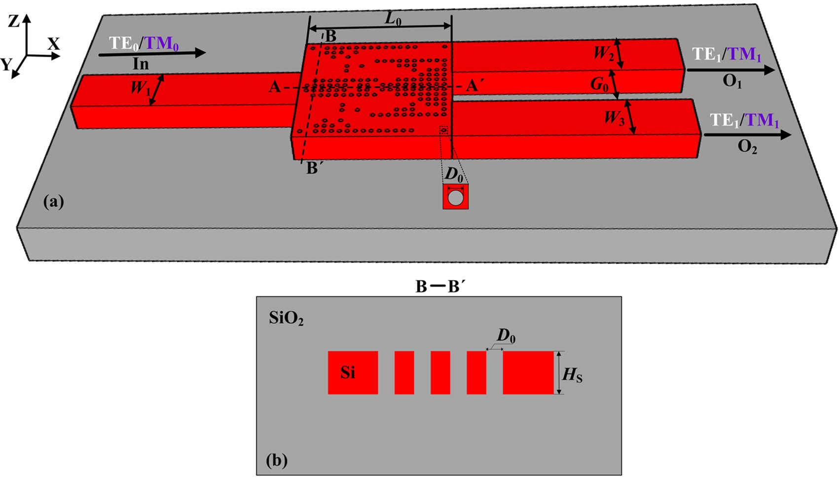
Figure 1(a) describes a schematic drawing of our introduced PIMCPS consisting of an input strip waveguide, a pixelated region, and two output strip waveguides. This device is designed to be axisymmetric along line . The widths of the input waveguide and the two output waveguides are labeled as , , and , which are chosen as to support the , , , and modes. The spacing between the two output waveguides is denoted by , which is set as . The length of the pixelated region is marked as , which is chosen to be 4 µm. In the pixelated region, there are identical pixels. Each pixel’s shape is a square of with a central circular hole, where the diameter is 100 nm and its logic state can be “1” or “0”, standing for the hole filled with or Si. The cross-sectional view of the pixelated region is illustrated in Fig. 1(b). The thickness of the silicon waveguide is 220 nm. By defining the logic states of the pixels to tune the refractive index distribution and control the behavior of the optical field, the input () mode from the In port would be transformed into the () mode after passing through the pixelated region, and the () mode uniformly exits from the two output ports and . In order to convert and split the targeted modes within a compact length more efficiently, the DBS optimization algorithm and the FDTD method are employed to optimize each pixel’s logic state. The optimization figure of merit (FoM) is written as

Fig. 1. (a) Schematic drawing of our introduced PIMCPS. (b) Cross-sectional view of the pixelated region along line B-B’.
According to the above optimization steps, it takes approximately 36 hours to realize the optimized logic states of the pixels by adopting a computer with a 16-core central processing unit (Inter Core i7-10700K).
The simulated light propagation in the optimized PIMCPS is shown in Fig. 2. As the and modes are injected into the In port, they are converted into and modes. Then, the and modes are evenly separated and come out from the two output ports and . In other words, the corresponding functionality of the optimized PIMCPS can be executed well.

Fig. 2. Simulated light propagation in the optimized PIMCPS with input (a) TE0 or (b) TM0 mode.
Figure 3 shows the CT, IL, and PU of our optimized PIMCPS as a function of the wavelength. As seen in Fig. 3, within a BW from 1518 to 1611 nm, for the optimized PIMCPS in TE polarization, , , are obtained, while in the case of the optimized PIMCPS in TM polarization, , , and are achieved. At 1550 nm, in TE polarization, the designed PIMCPS can have a CT of , an IL of 0.28 dB, and a PU of 0.00308, while in TM polarization, the CT, IL, and PU are , 0.45 dB, and 0.00028 dB, respectively. The corresponding IL, CT, and PU are defined as
Figure 4 depicts the IL, CT, and PU of our optimized PIMCPS as a function of the waveguide width variation and the diameter variation at 1550 nm. As seen in Fig. 4, different values of and have an impact on the IL, CT, and PU of the designed PIMCPS. As varies from to 20 nm and is set to be 20 nm, 15 nm, 10 nm, 0 nm, , , or , , , and are realized in TM polarization, while in TE polarization, the calculated IL, CT, and PU are less than 1.62 dB, , and 0.097 dB, respectively.

Fig. 4. (a), (b) IL, (c), (d) CT, and (e), (f) PU of the designed PIMCPS changing with ΔW and ΔD when the output modes are TM1 and TE1 modes.
3. Fabrication and Characterization
By taking advantage of electron-beam lithography, two-step inductively coupled plasma dry etching, and plasma-enhanced chemical vapor deposition processes, we fabricated the optimized PIMCPSs. Figure 5 depicts the microscopic image of the fabricated PIMCPSs and the relevant two-mode demultiplexers.
A tunable semiconductor laser (SANTEC TSL-550) and a multi-port optical powermeter (SANTEC MPM-210) are employed for characterizing the performance of the fabricated PIMCPSs. To couple the TM-polarized or the TE-polarized light beam into and out of the fabricated devices, the focusing grating coupler or photonic crystal structure is adopted, respectively. The measured transmission of the presented PIMCPS would be normalized by subtracting the transmission of the relevant two-mode demultiplexer. Figure 6 illustrates the measured CT, IL, and PU of the fabricated PIMCPS as a function of the wavelength. Note that in Fig. 6, at 1550 nm, the measured IL, CT, and PU are respectively 0.57 dB, , and 0.094 dB in TE polarization. In TM polarization, the measured IL, CT, and PU are 0.57 dB, , and 0.11 dB, respectively. Within a BW from 1520 to 1600 nm, in TE polarization, the measured IL, CT, and PU are smaller than 1.39 dB, , and 0.14 dB, respectively, while in TM polarization, the measured IL, CT, and PU are lower than 1.23 dB, , and 0.14 dB, respectively. The measured IL, CT, PU, and BW are also slightly worse than that in the simulation. The reasons are described below.

Fig. 6. Measured CT, IL, and PU of the fabricated PIMCPS as a function of the wavelength.
On the one hand, the actual fabricated waveguide width and diameter could deviate from the optimum ones in the simulation on different levels, causing the slight deteriorations of IL, CT, and PU. On the other hand, the BW obtained from the measurement is not as wide as the one in the simulation owing to the limitations of the light source used. Table 1 lists the performance of the fabricated polarization-insensitive mode-order converters (PIMOCs)[4,9], polarization-insensitive power splitters (PIPSs)[12,14], and polarization-insensitive mode-order converting power splitter. As illustrated in Table 1, compared with other devices, our PIMCPS can have a compact size, a broad BW, a relatively small IL, a low CT, and an excellent PU. In the future, high-quality and high-accuracy fabrication processes could be used to further enhance the performance of our proposed PIMCPS.
Table 1. Performance Comparison of the Proposed PIMCPS, the Reported PIMOCs, and the PIPSs
| ||||||||||||||||||||||||||||||||||||||||||||||
4. Conclusion
In conclusion, a PIMCPS using a pixelated region has been proposed, designed, and experimentally demonstrated. The DBS algorithm and FDTD method are employed to optimize the structural parameters of the pixelated region to achieve polarization-insensitive property, compact footprint, wide BW, small IL, low CT, and excellent PU. Measurement results reveal that, for the fabricated PIMCPS at 1550 nm, the CT, IL, and PU are , 0.57 dB, and 0.094 dB, respectively, in TE polarization, while in TM polarization, the CT, IL, and PU are , 0.57 dB, and 0.11 dB, respectively. Within a wavelength range from 1520 to 1600 nm, the CT, IL, and PU of the fabricated PIMCPS working at TE polarization are less than , 1.39 dB, and 0.14 dB. For the fabricated PIMCPS working at TM polarization, the CT, IL, and PU are lower than , 1.23 dB, and 0.14 dB. The length of the pixelated region is only 4 µm. With the above-mentioned characteristics, our introduced PIMCPS provides an attractive option for constructing an on-chip MDM transmission system.
Article Outline
Haoqi Chen, Runkui Yao, Pengjun Wang, Qiang Fu, Weiwei Chen, Shixun Dai, Dejun Kong, Jian Lin, Tao Jin, Jun Li, Tingge Dai, Jianyi Yang. Ultra-compact and broadband polarization-insensitive mode-order converting power splitter[J]. Chinese Optics Letters, 2024, 22(3): 031301.


