基于分子间电荷转移效应的P3HT∶Y6基可近红外响应有机光电倍增探测器
The photomultiplication organic photodetector based on trap-assisted carrier tunneling mechanism not only has high sensitivity but also simplifies system design and effectively improves the weak light detection performance of the photodetector. At present, photomultiplication organic photodetectors mainly focus on the visible range and have relatively few responses in the near-infrared region. Detection in the near-infrared region has broad application prospects in many fields and the demand is becoming increasingly urgent. Intermolecular charge transfer is a low-cost method for achieving near-infrared absorption in organic photomultiplier detectors, which can effectively expand the response band of devices. However, the absorption is low and the response is very weak at long wavelengths. The photomultiplication type devices can amplify weak photocurrent signals and improve device performance. Therefore, by introducing a small amount of organic acceptor Y6 in the P3HT active layer, we fabricate a photomultiplication type organic photodetector. Due to the intermolecular charge transfer between P3HT and Y6, the response band of the device can be extended to 1310 nm, which is superior to the reported near-infrared multiplication type organic photodetectors. By introducing an atomic level thickness of Al2O3 between the hole transport layer and the active layer, the device can work under both positive and negative biases. The external quantum efficiency of the device at 860 nm reaches 800%, with a detectivity of 5.6×10¹¹ Jones. The external quantum efficiency of the device at 1310 nm reaches 80.4%, and the specific detectivity reaches 5.13×10¹⁰ Jones. This work can promote the development of near-infrared photomultiplication organic photodetector.
Firstly, the cleaned ITO substrates are dried by nitrogen gas and transferred to a glove box. PEDOT∶PSS is diluted with anhydrous ethanol in a volume ratio of 1∶9 and is span-coated onto the ITO substrate to form a hole transport layer. Then, the Al2O3 interface modification layer is deposited by atomic layer deposition equipment. Subsequently, the active layer is formed by spin-coating P3HT∶Y6 mixture solution, with a P3HT and Y6 ratio of 100∶1 in weight. Finally, the Al electrode is deposited on the active layer by thermal evaporation. The bright and dark currents of the device are obtained by a digital source meter Keithley 2400 and different light sources in a sealed and room temperature state. The testing of external quantum efficiency and responsiveness is performed in a dark shielding box, with ITO as the anode connecting to the positive pole of the power supply and Al as the cathode connecting to the negative pole. The digital source meter Keithley 2400 is adopted to apply different voltages, and a femtosecond laser is utilized as the light source. The light intensity is attenuated to a specified size by an attenuation plate, and the dark current and bright state J-V curves under different light sources are collected. Finally, the external quantum efficiency and responsivity data are obtained through calculation (the data has been background deducted). The linear dynamic range, noise current, and specific detection rate of the device are tested, and the performance of the device is comprehensively analyzed. A spectrophotometer instrument is leveraged to characterize the ultraviolet visible near-infrared absorption spectrum. In addition, the transmission spectrum, reflection spectrum, and film thickness of the device are also tested.
Al2O3 modified device with a structure of ITO/PEDOT∶PSS/Al2O3/P3HT∶Y6 (100∶1)/Al and a control device without Al2O3 are both fabricated. We verify that the Al2O3 interface modification layer can greatly reduce the dark current of the device and enable the device to achieve bidirectional bias response (Fig. 1). Next, the Al2O3 modified device is characterized, and the device can respond to 1310 nm. The weak light detection limit of the device at 505 nm can reach 7.8 nW/cm2. When the optical power density is 3.8×10⁻⁴ mW/cm2, the external quantum efficiency of the device at 860 nm is 800%, with a specific detectivity of 5.6×10¹¹ Jones. When the optical power density is 3.67×10⁻² mW/cm2, the external quantum efficiency of the device at 1310 nm is 80.4%, with a specific detectivity of 5.13×10¹⁰ Jones. Under the irradiation of visible light at 505 nm and near-infrared light at 860 nm, the device has a dynamic range of over 125 dB and 90 dB, respectively (Fig. 2 and Fig. 3). The comprehensive performance of the device has certain advantages compared to the near-infrared organic photomultiplier detectors prepared in recent years. By introducing an organic receptor Y6 with light absorption ability in the near-infrared region, the device effectively promotes the injection of holes from external currents as an electron trap and interacts with P3HT, expanding the corresponding band and achieving high sensitivity detection in the near-infrared region (Fig. 4).
A low-cost and highly sensitive near-infrared photomultiplication organic photodetector with a structure of ITO/PEDOT∶PSS/Al2O3/P3HT∶Y6/Al is reported. By adding Al2O3 as an interface modification layer, the dark current of the device is significantly reduced, resulting in a device that can respond in both forward and reverse bias directions. Adding a small amount of Y6 to the active layer can achieve a wide spectral response from UV visible to near-infrared, and the response wavelength can be extended to 1310 nm. The external quantum efficiency of the device at 860 nm reaches 800%, with a specific detectivity of 5.6×10¹¹ Jones. The external quantum efficiency of the device at 1310 nm reaches 80.4%, and the specific detectivity reaches 5.13×10¹⁰ Jones. These properties have certain advantages in reported near-infrared photomultiplication organic photodetector and can promote the development of near-infrared photomultiplication organic photodetectors.
1 引言
光电探测器是一种能将入射光信号转化为电信号的光电子器件[1],在火焰和辐射检测、图像传感[2]、健康监测[3]、光纤通信[4]等领域都有着广泛的应用。传统的光电探测器一般基于硅、锗、砷化镓等无机半导体材料进行制备,它们不仅制备过程复杂、成本高昂,而且机械柔韧性较差[5]。相比而言,有机光电探测器具有成本低、质量轻、易于大面积加工[6]等优势,且与柔性衬底有更好的兼容性[7],在柔性电子皮肤、可穿戴设备、生物医学成像等新兴领域的应用前景广阔[8]。
目前,有机光电探测器发展迅速,已经可以探测紫外、可见、近红外波段的光信号[9-12]。许多领域如医学检测、食品监测对近红外探测的需求日益迫切,因此,可近红外响应的有机光电探测器成为研究的一大热点[13-14]。近年来,得益于窄带隙给体材料和非富勒烯受体材料的发展,近红外有机光电探测器得到了快速的发展[15-16]。基于陷阱辅助载流子隧穿机理的倍增型有机光电探测器由于外量子效率(EQE)大、响应度高受到了研究人员的重视[17-19],可近红外响应的有机光电倍增探测器已有很多报道[20]。2021年,Han等[17]制备了以PBDB-9T∶Y6为活性层的器件,可以在300~900 nm波长范围内响应,在790 nm处外量子效率达到66,比探测率达到4.9×10¹² Jones。2021年,Liu等[2]采用P3HT、BEH、PTB7-Th、F6TCNNQ来制备倍增型有机光电探测器,器件可以在300~900 nm波长范围内响应,在850 nm处外量子效率达到150,响应度为0.1 A/W,比探测率达到8.8×1011 Jones。目前,近红外有机光电倍增探测器的研究取得了不错的进展,但活性层大多采用价格高昂的窄带隙给体及受体材料,这就提高了器件的成本。此外,已报道的近红外有机光电倍增探测器的探测波长大多在1000 nm以下[21-23]。
基于分子间电荷转移的近红外有机光电探测器,利用给体/受体材料分子间电荷转移(CT)吸收原理直接将吸收波段拓展至短波红外区域,但面临着吸收低、响应弱的问题,而采用倍增器件结构可以放大微弱的光电流信号,提升器件的性能[24]。据此,本文制备了结构为ITO/PEDOT∶PSS/Al2O3/P3HT∶Y6(100∶1)/Al的倍增型近红外有机光电探测器,通过在成本较低的活性层P3HT中少量引入在近红外波段有吸光能力的有机受体Y6,实现了器件在近红外波段的响应,降低了器件的成本,并通过P3HT与Y6之间的分子间电荷转移效应,器件的响应波段可拓展至1310 nm。同时,在器件中加入原子级厚度的Al2O3,有效抑制了暗电流,从而将器件由只能反向偏压响应改善到能够正反双向偏压响应。研究结果表明:当光功率密度为3.8×10⁻⁴ mW/cm2时,器件在860 nm处的外量子效率为800%,比探测率为5.6×10¹¹ Jones;当光功率密度为3.67×10⁻² mW/cm2时,器件在1310 nm处的外量子效率为80.4%,比探测率为5.13×10¹⁰ Jones。这些性能在目前所报道的近红外倍增型有机光电探测器中具有一定优势。
2 实验
2.1 样品制备
氧化铟锡(ITO)基底的处理:采用商业化刻蚀后带有ITO图形的玻璃衬底,制备出有效面积为0.2 cm×0.2 cm的光电倍增探测器。将ITO用洗洁精和洗涤剂搓洗以去除表面污渍,随后用去离子水冲洗,并分别置于丙酮、无水乙醇、异丙醇溶液中超声15 min,用氮气吹干后移到手套箱。
空穴传输层PEDOT∶PSS(聚(3,4-乙烯二氧噻吩)-聚苯乙烯磺酸)的制备:首先,将PEDOT∶PSS与无水乙醇按照1∶9的体积比稀释,用1 mL针管吸取一定量PEDOT∶PSS并加装合适的滤头,旋涂在处理好的 ITO 基底上,转速为9000 r/min,匀胶时间为30 s;然后,置于120 ℃热台上退火15 min。
Al2O3界面修饰层的制备:利用原子层沉积设备在真空150 ℃下使Al(CH3)3和H2O交替反应,以0.1 nm/cycle的速率沉积厚度为0.8 nm的Al2O3,结束后冷却3 min待用。
活性层的制备:将P3HT(3-己基取代聚噻吩)和Y6(2,20-((2Z,20Z)-((12,13-双(2-乙基己基)-3,9-双十一烷-12,13-二氢-[1,2,5]噻二唑[3,4-e]噻吩并[2″,30':4',50]噻吩并[20,30:4,5]吡咯并[3,2-g]噻吩并[20,30:4,5]噻吩并[3,2-b]吲哚-2,10-二基)双-(2-甲烯基))-(3-1,1-甲烯丙二腈)-5,6-二氟茚酮))按照100∶1的质量比溶于邻二氯苯,配置40 mg/mL的溶液。将30 μL的P3HT∶Y6溶液旋涂在ITO/PEDOT∶PSS/Al2O3的玻璃片上,转速为1000 r/min,时间为30 s,旋涂完毕后立即置于80 ℃热台退火20 s,结束后冷却3 min待用。
金属电极的制备:利用蒸镀设备在10-4 Pa的高真空下蒸镀 100 nm 厚度的Al 电极。
2.2 测试与表征
对制备的近红外有机光电倍增探测器的性能表征指标主要有:光照及暗态下的电流密度-电压(J-V)曲线、外量子效率、响应度、噪声电流、比探测率、线性动态范围、瞬态响应曲线、紫外-可见-近红外吸收光谱及膜厚等。
光电测试系统所在实验环境为密闭且室温状态,利用数字源表Keithley 2400获得器件的电流,光源采用不同波长的LED光源(如375、505、660、850 nm)及激光器(如980 nm、1310 nm);外量子效率和响应度的测试是将器件放置在暗箱屏蔽箱中,ITO作为器件阳极接电源正极,Al作为阴极接电源负极,对数字源表Keithley 2400施加不同电压,并利用飞秒激光器作为光源,使用衰减片将光强衰减到指定大小,采集暗电流和不同光源下的亮态J-V曲线,并通过计算获得外量子效率和响应度数据(数据已作背景扣除)。利用频谱分析仪与安捷伦 B2961 连接测试噪声电流,由安捷伦B2900A采集数据;利用信号发生器和安捷伦B2900A测试瞬态响应曲线;利用分光光度计采集紫外-可见-近红外吸收光谱,同时结合自动宏观角分辨光谱仪R1辅助测试器件的透射谱及反射谱;利用台阶仪测试薄膜厚度。
3 分析与讨论
3.1 Al2O3界面修饰层在器件中的作用
制备了ITO/PEDOT∶PSS/Al2O3/P3HT∶Y6(100∶1)/Al(Al2O3修饰器件)以及ITO/PEDOT∶PSS/P3HT∶Y6(100∶1)/Al(标准器件)两种器件,器件结构如
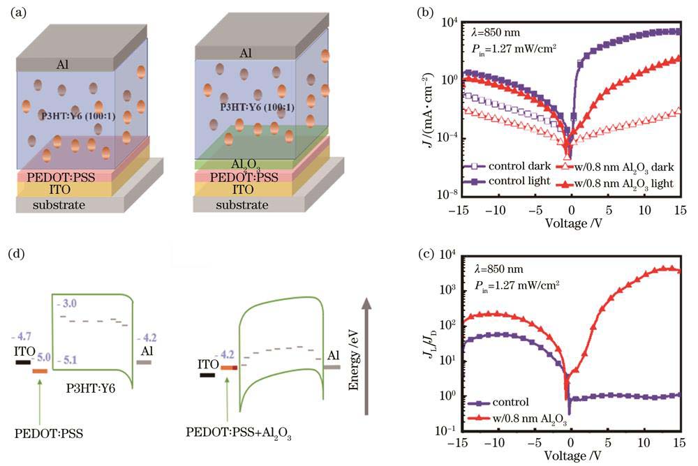
图 1. 不含与含Al2O3界面修饰层的器件结构及性能。(a)两种类型器件的结构;(b)两种类型器件在850 nm(1.27 mW/cm2)下的J-V曲线;(c)两种类型器件在850 nm(1.27 mW/cm2)下的亮暗电流比曲线;(d)两种类型器件的能级图
Fig. 1. Structure and performance of devices without and with Al2O3. (a) Structure diagram of two devices; (b) J-V curves of two devices at 850 nm (1.27 mW/cm2); (c) light-to-dark current ratio curves of two devices at 850 nm (1.27 mW/cm2); (d) energy level diagrams of two devices
为了分析工作机理及Al2O3界面修饰层的作用,对能带图进行分析,如
使用0.8 nm 厚的Al2O3修饰后,PEDOT∶PSS的功函数值出现明显变化,由5.0 eV减小到4.2 eV[25]。P3HT和Al2O3修饰后的PEDOT∶PSS的功函数相差0.8 eV,形成了如
3.2 器件性能表征
接下来对Al2O3修饰器件进行性能表征。
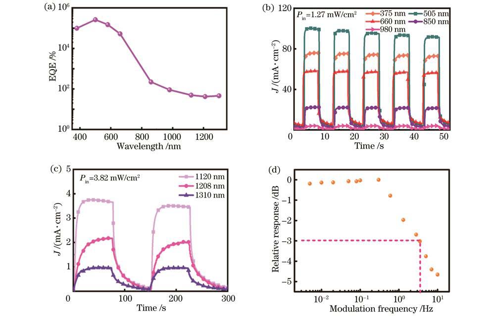
图 2. Al2O3修饰器件在15 V偏压下的相关表征。(a)外量子效率光谱;(b)瞬态响应曲线;(c)1120、1208、1310 nm光源照射下的瞬态响应曲线;(d)调制光源下的f-3 dB测试结果
Fig. 2. Characterization of Al2O3 modified device under 15 V bias voltage. (a) EQE spectrum; (b) transient response curves; (c) transient response curves under 1120, 1208, and 1310 nm light source irradiation; (d) f-3 dB measurement results under modulated light source
此外,还测试了器件在505、860、1310 nm光照射下器件的动态范围、外量子效率、响应度和比探测率曲线,如
式中:
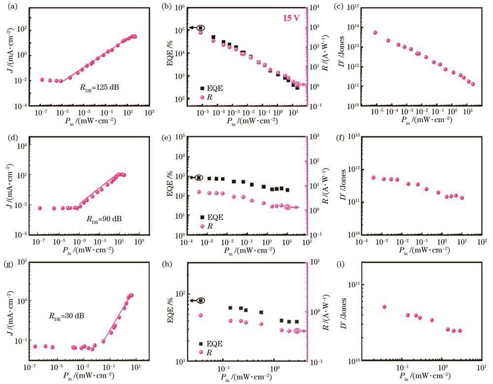
图 3. Al2O3修饰器件在不同光强下的相关表征。(a)505 nm光源下的动态范围;(b)505 nm光源下动态范围内的外量子效率和响应度;(c)505 nm光源下动态范围内的比探测率;(d)860 nm光源下的动态范围;(e)860 nm光源下动态范围内的外量子效率和响应度;(f)860 nm光源下动态范围内的比探测率;(g)1310 nm光源下的动态范围;(h)1310 nm光源下动态范围内的外量子效率和响应度;(i)1310 nm光源下动态范围内的比探测率
Fig. 3. Characterizations of Al2O3 modified device under different light intensities. (a) Dynamic range under 505 nm light source; (b) EQE and responsibility under 505 nm light source within dynamic range; (c) specific detectivity under 505 nm light source within dynamic range; (d) dynamic range under 860 nm light source; (e) EQE and responsibility under 860 nm light source within dynamic range; (f) specific detectivity under 860 nm light source within dynamic range; (g) dynamic range under 1310 nm light source; (h) EQE and responsibility under 1310 nm light source within dynamic range; (i) specific detectivity under 1310 nm light source within dynamic range
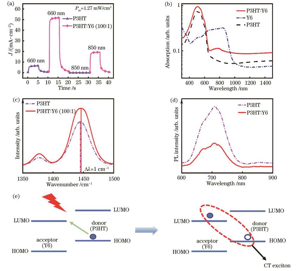
图 4. 器件的机理分析图。(a)纯P3HT器件及P3HT∶Y6器件的瞬态响应曲线;(b)P3HT、Y6及P3HT∶Y6(100∶1)的吸收光谱;(c)P3HT和P3HT∶Y6(100∶1)的拉曼光谱;(d)P3HT和 P3HT∶Y6(100∶1)在325 nm光源激发时的光致发光光谱;(e)分子间电荷转移形成原理示意图
Fig. 4. Mechanism analysis diagram of the device. (a) Transient response curves of pure P3HT thin film as active layer and Al2O3 modified devices; (b) absorption spectra of P3HT, Y6, and P3HT∶Y6 (100∶1); (c) Raman spectra of P3HT and P3HT∶Y6 (100∶1); (d) photoluminescence spectra of P3HT and P3HT∶Y6 (100∶1) excited by a 325 nm light source; (e) principle schematic of intermolecular charge transfer formation
3.3 器件机理分析
为了分析器件在长波段响应的原因,制备了Al2O3修饰的P3HT∶Y6活性层器件,并和纯P3HT作为活性层的器件进行对比分析,结果如
为了更好地分析器件性能产生的机理,测试了拉曼光谱和光致发光光谱。
基于上述测试与分析,验证了器件的近红外性能主要来源于Y6的掺杂,并且通过采用P3HT∶Y6作为活性层,利用Y6的红外吸收特性以及P3HT与Y6之间的相互作用,实现了在近红外区域的高灵敏探测。
4 结论
制备了一种结构为ITO/PEDOT∶PSS/Al2O3/P3HT∶Y6/Al的低成本、高响应度的近红外有机光电倍增探测器,通过加入Al2O3作为界面修饰层,显著降低了器件的暗电流,得到能够正反偏压双向响应的器件。在活性层中添加少量的Y6可实现紫外-可见-近红外的宽光谱响应,基于P3HT和Y6之间发生的分子间电荷转移作用,响应波长可拓展至1310 nm。器件在860 nm处的外量子效率可达800%,比探测率为5.6×10¹¹ Jones;器件在1310 nm处的外量子效率达到80.4%,比探测率可达5.13×10¹⁰ Jones。这些性能在已报道的近红外有机光电倍增探测器中具有一定优势,可促进低成本近红外有机光电倍增探测器的发展。
[1] Guo D C, Yang L Q, Li J, et al. Panchromatic photomultiplication-type organic photodetectors with planar/bulk heterojunction structure[J]. Science China Materials, 2023, 66(3): 1172-1179.
[2] Liu M, Wang J, Zhao Z J, et al. Ultra-narrow-band NIR photomultiplication organic photodetectors based on charge injection narrowing[J]. The Journal of Physical Chemistry Letters, 2021, 12(11): 2937-2943.
[3] Nath D, Dey P, Joseph A M, et al. Zero bias high responsive visible organic photodetector based on pentacene and C60[J]. Optics & Laser Technology, 2020, 131: 106393.
[4] Agostinelli T, Caironi M, Natali D, et al. A planar organic near infrared light detector based on bulk heterojunction of a heteroquaterphenoquinone and poly [2-methoxy-5-(2′-ethyl-hexyloxy)-1, 4-phenylene vinylene][J]. Journal of Applied Physics, 2008, 104(11): 114508.
[5] Zhou X K, Yang D Z, Ma D G, et al. Ultrahigh gain polymer photodetectors with spectral response from UV to near-infrared using ZnO nanoparticles as anode interfacial layer[J]. Advanced Functional Materials, 2016, 26(36): 6619-6626.
[6] Yang L Q, Guo D C, Li J, et al. Low-cost copper electrode for high-performance panchromatic multiplication-type organic photodetectors with optical microcavity effect[J]. Advanced Functional Materials, 2022, 32(20): 2108839.
[7] Wang J B, Zheng Q D. Enhancing the performance of photomultiplication-type organic photodetectors using solution-processed ZnO as an interfacial layer[J]. Journal of Materials Chemistry C, 2019, 7(6): 1544-1550.
[8] 翁思远, 蒋大勇, 赵曼. P3HT∶PC61BM作为活性层制备无机/有机异质结光电探测器的研究[J]. 光学学报, 2022, 42(13): 1304001.
[9] Zhang X R, Jiang J Z, Feng B G, et al. Organic photodetectors: materials, device, and challenges[J]. Journal of Materials Chemistry C, 2023, 11(37): 12453-12465.
[10] Zhao Z J, Xu C Y, Niu L B, et al. Recent progress on broadband organic photodetectors and their applications[J]. Laser & Photonics Reviews, 2020, 14(11): 2000262.
[11] Yang D Z, Ma D G. Development of organic semiconductor photodetectors: from mechanism to applications[J]. Advanced Optical Materials, 2019, 7(1): 1800522.
[13] 薛晓梦, 马海菲, 郝群, 等. 高载流子迁移率胶体量子点红外探测器[J]. 光学学报, 2023, 43(22): 2204002.
[14] 郝群, 唐鑫, 陈梦璐. 硫汞族量子点红外光电探测技术[J]. 光学学报, 2023, 43(15): 1500001.
[15] Winkler L C, Kublitski J, Benduhn J, et al. Photomultiplication enabling high-performance narrowband near-infrared organic photodetectors[J]. Advanced Electronic Materials, 2023, 9(9): 2201350.
[16] Li Q Y, Guo Y L, Liu Y Q. Exploration of near-infrared organic photodetectors[J]. Chemistry of Materials, 2019, 31(17): 6359-6379.
[17] Han S G, Lee H, Choi W, et al. Photomultiplication-type organic photodetectors with fast response enabled by the controlled charge trapping dynamics of quantum dot interlayer[J]. Advanced Functional Materials, 2021, 31(31): 2102087.
[18] 安涛, 吴禧梅, 刘欣颖. 基于双掺杂C60∶DDQ陷阱的倍增型有机光电探测器[J]. 光子学报, 2020, 49(10): 1025001.
[19] An T, Liu X Y. Broadband organic color photodetectors with high gain based on C60-doped tri-phase bulk heterojunction[J]. Journal of Materials Science: Materials in Electronics, 2020, 31(4): 2757-2765.
[20] 高秀云, 张叶, 崔艳霞, 等. 有机光电倍增探测器研究进展[J]. 激光与光电子学进展, 2018, 55(7): 070001.
[21] Tao S Z, Yang D Z, He G, et al. Photomultiplication-type perovskite photodetectors base on air-processed perovskite films[J]. Organic Electronics, 2023, 118: 106800.
[22] Yang K X, Zhao Z J, Liu M, et al. Employing liquid crystal material as regulator to enhance performance of photomultiplication type polymer photodetectors[J]. Chemical Engineering Journal, 2022, 427: 131802.
[23] Wang W B, Zhang F J, Bai H T, et al. Photomultiplication photodetectors with P3HT: fullerene-free material as the active layers exhibiting a broad response[J]. Nanoscale, 2016, 8(10): 5578-5586.
[24] Kublitski J, Fischer A, Xing S, et al. Enhancing sub-bandgap external quantum efficiency by photomultiplication for narrowband organic near-infrared photodetectors[J]. Nature Communications, 2021, 12: 4259.
[25] Shi L L, Zhu Y Z, Li G H, et al. Atomic-level chemical reaction promoting external quantum efficiency of organic photomultiplication photodetector exceeding 108% for weak-light detection[J]. Science Bulletin, 2023, 68(9): 928-937.
[26] Yamamoto J, Furukawa Y. Raman characterization and electrical properties of poly (3-hexylthiophene) doped electrochemically in an ionic liquid-gated transistor geometry[J]. Organic Electronics, 2016, 28: 82-87.
[27] Stylianakis M M, Stratakis E, Koudoumas E, et al. Organic bulk heterojunction photovoltaic devices based on polythiophene-graphene composites[J]. ACS Applied Materials & Interfaces, 2012, 4(9): 4864-4870.
[28] Wang T, Lu Y, Xu L, et al. π‑conjugated poly (3-hexylthiophene-2, 5-diyl) thin film as a SERS substrate for molecule detection application[J]. Journal of Materials Science, 2022, 57(35): 16965-16973.
[29] Yin H, Tian T, Zhang R X, et al. High-performance broadband photodetectors based on asymmetric all-carbon nano-heterostructures[J]. ACS Applied Nano Materials, 2023, 6(13): 11934-11943.
[30] Xu Z H, He M, Wu Q K, et al. Ultrafast charge transfer 2D MoS2/organic heterojunction for sensitive photodetector[J]. Advanced Science, 2023, 10(12): 2207743.
[31] Iqbal M A, Liaqat A, Hussain S, et al. Ultralow-transition-energy organic complex on graphene for high-performance shortwave infrared photodetection[J]. Advanced Materials, 2020, 32(37): 2002628.
[32] Kim J H, Liess A, Stolte M, et al. An efficient narrowband near-infrared at 1040 nm organic photodetector realized by intermolecular charge transfer mediated coupling based on a squaraine dye[J]. Advanced Materials, 2021, 33(26): 2100582.
[33] Gibert-Roca M, Molet P, Mihi A, et al. Near infrared organic photodetectors based on enhanced charge transfer state absorption by photonic architectures[J]. Journal of Materials Chemistry C, 2020, 8(28): 9688-9696.
胡依凡, 滑羽璐, 冀婷, 石林林, 崔艳霞, 李国辉. 基于分子间电荷转移效应的P3HT∶Y6基可近红外响应有机光电倍增探测器[J]. 光学学报, 2024, 44(4): 0404001. Yifan Hu, Yulu Hua, Ting Ji, Linlin Shi, Yanxia Cui, Guohui Li. P3HT∶Y6-Based Near-Infrared Organic Photomultiplication Photodetectors by Intermolecular Charge Transfer Effects[J]. Acta Optica Sinica, 2024, 44(4): 0404001.
