基于感光栅极GaN高迁移率晶体管的新型探测器制备与优化  下载: 518次
Preparation and Optimization of Photosensitive Gate GaN-based High Electron Mobility Transistor Devices
北京工业大学 光电子技术教育部重点实验室, 北京 100124
图 & 表
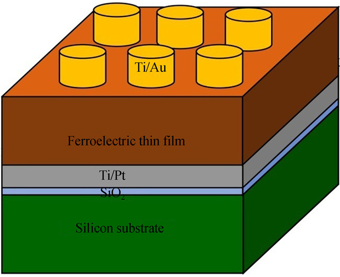
图 1.
Fig. 1. Schematic diagram of PZT preparation structure
下载图片 查看原文
图 3.
Fig. 3. XRD analysis chart of different growth conditions
下载图片 查看原文
图 4.
Fig. 4. Analysis of hysteresis loops for different growth conditions
下载图片 查看原文
图 5.
Fig. 5. Schematic diagram of the PZT/GaN-based HEMT detector structure
下载图片 查看原文
图 6.
Fig. 6. Illustration of the steps relevant to the fabrication of the grating electrode GaN-based HEMT device structure
下载图片 查看原文
图 7.
Fig. 7. Dark and UV light output characteristic curves for the tested GaN-based HEMT devices
下载图片 查看原文
图 8.
Fig. 8. Optical micrograph of the three kinds of different gate length devices
下载图片 查看原文
图 9.
Fig. 9. Characteristic curves of the three different gate length devices
下载图片 查看原文
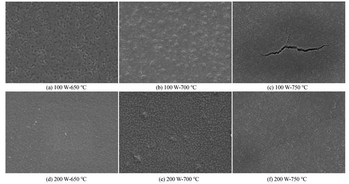
表 1PZT film experimental sample process parameters
Table1. PZT film experimental sample process parameters
| Experimental sample | Sputtering power/W | Working pressure /Pa | Sputtering time/h | | 1 | 100 | 1 | 1.50 | | 2 | 200 | 1 | 0.75 |
|
查看原文
表 2Annealing process parameters
Table2. Annealing process parameters
| Experimental sample | Annealing temperature/℃ | Annealing time/min | | 1-A | 650 | 3 | | 1-B | 700 | 3 | | 1-C | 750 | 3 | | 2-A | 650 | 3 | | 2-B | 700 | 3 | | 2-C | 750 | 3 |
|
查看原文
表 3Parameter results of Fig. 4(a)
Table3. Parameter results of Fig. 4(a)
| Annealing temperature/℃ | Saturation polarization/(μC·cm-2) | Remnant polarization/(μC·cm-2) | Coercive field/(kV·cm-1) | | 650 | 30.6 | 9.3 | 37.0 | | 700 | 65.3 | 20.4 | 31.5 | | 750 | 50.8 | 12.4 | 33.7 |
|
查看原文
表 4Parameter results of Fig. 4(b)
Table4. Parameter results of Fig. 4(b)
| Annealing temperature/℃ | Saturation polarization/(μC·cm-2) | Remnant polarization/(μC·cm-2) | Coercive field/(kV·cm-1) | | 650 | 36.0 | 7.1 | 32.3 | | 700 | 84.0 | 38.0 | 37.3 | | 750 | 62.6 | 17.4 | 30.5 |
|
查看原文
表 5Device structure parameters for the three different gate lengths
Table5. Device structure parameters for the three different gate lengths
| Sample label | Gate length(LG/μm) | Gate source spacing(LGS/μm) | Gatedrain spacing(LGD/μm) | | A | 1 | 3 | 4 | | B | 2 | 3 | 4 | | C | 3 | 3 | 4 |
|
查看原文
朱彦旭, 朱彦旭, 杨壮, 宋会会, 李赉龙, 杨忠, 李锜轩, 胡铁凡. 基于感光栅极GaN高迁移率晶体管的新型探测器制备与优化[J]. 光子学报, 2020, 49(6): 0604002. Yan-xu ZHU, Yan-xu ZHU, Zhuang YANG, Hui-hui SONG, Lai-long LI, Zhong YANG, Qi-xuan LI, Tie-fan HU. Preparation and Optimization of Photosensitive Gate GaN-based High Electron Mobility Transistor Devices[J]. ACTA PHOTONICA SINICA, 2020, 49(6): 0604002.


 PDF全文
PDF全文
