Author Affiliations
Abstract
1 College of Advanced Interdisciplinary Studies, National University of Defense Technology, Changsha 410073, China
2 Beijing Institute for Advanced Study, National University of Defense Technology, Beijing 100020, China
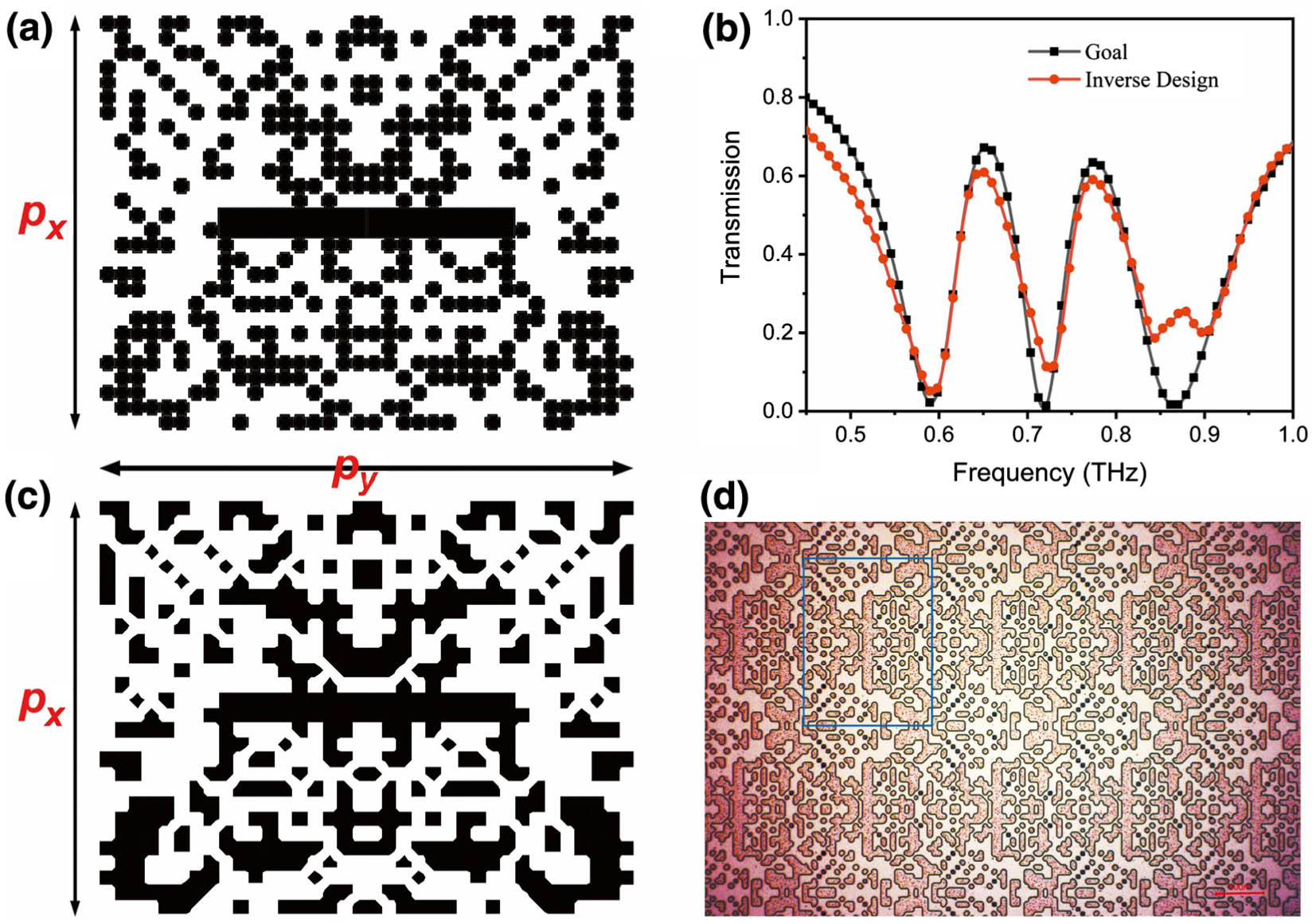
Terahertz metasurfaces have great applications for efficient terahertz modulation, but there are still problems in designing terahertz metadevices in terms of complexity and inefficiency. Herein, we demonstrate an inversely-designed terahertz metasurface with double electromagnetically induced transparency (EIT)-like windows by incorporating a particle swarm optimization (PSO) algorithm with the finite-difference time-domain method. We prepared and tested the metadevices, and the experimental terahertz signals are close to the designed results. By hybridizing amorphous germanium film with the inversely-designed metasurface, two EIT-like windows, including transmission and slow-light effect, exhibit ultrafast modulation behavior in 25 ps excited by a femtosecond laser. The modulation depths of transmission in two transparency windows are 74% and 65%, respectively. The numerical simulations also illustrate the ultrafast dynamic process and modulation mechanism, which match well with the experiment results. Our work thus offers opportunities for designing other objective functions of the terahertz metadevice.
terahertz metasurfaces inverse design double electromagnetically induced transparency Chinese Optics Letters
2022, 20(11): 113701

Author Affiliations
Abstract
1 College of Advanced Interdisciplinary Studies, National University of Defense Technology, Changsha 410073, China
2 Defense Innovation Institute, Academy of Military Sciences PLA China, Beijing 100071, China
3 Beijing Institute for Advanced Study, National University of Defense Technology, Beijing 100020, China
We present a theoretical analysis of a novel multi-channel light amplification photonic system on chip, where the nonlinear Raman amplification phenomenon in the silicon (Si) wire waveguide is considered. Particularly, a compact and temperature insensitive Mach–Zehnder interferometer filter working as demultiplexer is also exploited, allowing for the whole Si photonic system to be free from thermal interference. The propagation of the multi-channel pump and Stokes lights is described by a rigorous theoretical model that incorporates all relevant linear and nonlinear optical effects, including the intrinsic waveguide optical losses, first- and second-order frequency dispersion, self-phase and cross-phase modulation, phase shift and two-photon absorption, free-carriers dynamics, as well as the inter-pulse Raman interaction. Notably, to prevent excessive drift of the transmission window of the demultiplexer caused by ambient temperature variations and high thermo-optical coefficient of Si, an asymmetric waveguide width is adopted in the upper and lower arms of each Mach–Zehnder interferometer lattice cell. A Chebyshev half-band filter is utilized to achieve a flat pass-band transmission, achieving a temperature sensitivity of and over 100 K temperature span. This all-Si amplifier shows a thermally robust behavior, which is desired by future Si-on-insulator (SOI) applications.
Chinese Optics Letters
2022, 20(8): 081301
强激光与粒子束
2022, 34(1): 011010
二维过渡金属硫族化合物自旋-能谷特性是近年来国际研究热点之一。介绍了过渡金属硫族化合物材料以及其异质结中独特的自旋-能谷特性。阐述了这两大类材料中自旋-能谷特性的研究进展。最后对基于二维过渡金属硫族化合物自旋-能谷特性的未来光电器件进行了展望。
过渡金属硫族化合物 自旋-能谷特性 异质结 transition metal dichalcogenides spin-valley property heterostructure

Author Affiliations
Abstract
1 College of Advanced Interdisciplinary Studies, National University of Defense Technology, Changsha 410073, China
2 National Innovation Institute of Defense Technology, Academy of Military Sciences PLA China, Beijing 100071, China
3 State Key Laboratory of High Performance Computing, College of Computer, National University of Defense Technology, Changsha 410073, China
In this work, a soliton mode-locked erbium-doped fiber laser (EDFL) with a high-quality molecular beam epitaxy (MBE)-grown topological insulator (TI) Bi2Se3 saturable absorber (SA) is reported. To fabricate the SA device, a 16-layer Bi2Se3 film was grown successfully on a 100 μm thick SiO2 substrate and sandwiched directly between two fiber ferrules. The TI-SA had a saturable absorption of 1.12% and a saturable influence of 160 MW/cm2. After inserting the TI-SA into the unidirectional ring-cavity EDFL, self-starting mode-locked soliton pulse trains were obtained at a fundamental repetition rate of 19.352 MHz. The output central wavelength, pulse energy, pulse duration, and signal to noise ratio of the radio frequency spectrum were 1530 nm,18.5 pJ, 1.08 ps, and 60 dBm, respectively. These results demonstrate that the MBE technique could provide a controllable and repeatable method for the fabrication of identical high-quality TI-SAs, which is critically important for ultra-fast pulse generation.
140.4050 Mode-locked lasers 160.4236 Nanomaterials Chinese Optics Letters
2019, 17(7): 071403
Author Affiliations
Abstract
1 College of Advanced Interdisciplinary Studies, National University of Defense Technology, Changsha 410073, China
2 State Key Laboratory of High Performance Computing, College of Computer, National University of Defense Technology, Changsha 410073, China
3 Interdisciplinary Center of Quantum Information, National University of Defense Technology, Changsha 410073, China
4 National Institute of Defense Technology Innovation, Academy of Military Sciences PLA China, Beijing 100010, China
Broadband transient reflectivity traces were measured for Bi2Se3 thin films with various substrates via a 400 nm pump–white-light-probe setup. We have verified the existence of a second Dirac surface state in Bi2Se3 and qualitatively located it by properly analyzing the traces acquired at different probe wavelengths. Referring to the band structure of Bi2Se3, the relaxation mechanisms for photo-excited electrons with different energies are also revealed and studied. Our results show a second rise of the transient reflection signal at the time scale of several picoseconds. The types of substrate can also significantly affect the dynamics of the rising signal. This phenomenon is attributed to the effect of lattice heating and coherent phonon processes. The mechanism study in this work will benefit the fabrication of high-performance photonic devices based on topological insulators.
160.4236 Nanomaterials 300.6500 Spectroscopy, time-resolved Chinese Optics Letters
2019, 17(2): 020005
国防科技大学 前沿交叉学科学院,长沙 410073
新型半导体材料的发展是推动信息产业和光电产业发展的基石,探索新材料内在的物理机制是发展下一代光电器件的必然要求。作为太赫兹时域光谱的改进技术,时间分辨的太赫兹光谱探测是研究半导体瞬态光响应的有力支撑,文中将对光学泵浦太赫兹探测技术的原理、特点进行介绍。最后说明太赫兹超快光谱在物质科学领域的运用及发展趋势。
半导体材料 载流子动力学 超快光谱 太赫兹 semiconductor carrier dynamics ultrafast spectroscopy terahertz
1 国防科学技术大学机电工程与自动化学院, 湖南 长沙 410073
2 中国人民解放军 63880部队光电对抗试验和评估技术重点实验室, 河南 洛阳 471003
3 国防科学技术大学光电科学与工程学院, 湖南 长沙 410073
在飞秒单脉冲激光损伤 HfO2/SiO2薄膜样品实验中, 随着激光能量密度升高, 膜层从缺陷导致的点损伤发展到整层剥落, 损伤区域轮廓由模糊变清晰.研究表明, 尺度在纳米量级的颗粒缺陷会产生局部的场增强效应, 该效应与薄膜干涉场叠加, 造成了阈值损伤阶段损伤区域出现大量损伤点, 且由于飞秒激光对包括缺陷在内的薄膜材料的本征损伤特性, 使其损伤行为较为确定, 随着激光能量的提升, 薄膜出现更大面积的规则烧蚀区, 此时干涉场的作用上升到主导地位, 膜层的整层剥落行为掩盖了缺陷的诱导作用.
飞秒激光 光学薄膜 激光损伤 纳米颗粒缺陷 场增强效应 femtosecond laser optical coatings laser damage nanoscale particle defects light field intensification


