
Author Affiliations
Abstract
1 East China Normal University, School of Physics and Electronic Science, State Key Laboratory of Precision Spectroscopy, Shanghai, China
2 Nanjing University, College of Engineering and Applied Sciences, National Laboratory of Solid State Microstructures, Nanjing, China
3 China Jiliang University, College of Optical and Electronic Technology, Hangzhou, China
4 Shanxi University, Collaborative Innovation Center of Extreme Optics, Taiyuan, China
5 Chinese Academy of Sciences (CAS), Shanghai Institute of Optics and Fine Mechanics (SIOM), State Key Laboratory of High Field Laser Physics and CAS Center for Excellence in Ultra-Intense Laser Science, Shanghai, China
Achieving spatiotemporal control of light at high speeds presents immense possibilities for various applications in communication, computation, metrology, and sensing. The integration of subwavelength metasurfaces and optical waveguides offers a promising approach to manipulate light across multiple degrees of freedom at high speed in compact photonic integrated circuit (PIC) devices. Here, we demonstrate a gigahertz-rate-switchable wavefront shaping by integrating metasurface, lithium niobate on insulator photonic waveguides, and electrodes within a PIC device. As proofs of concept, we showcase the generation of a focus beam with reconfigurable arbitrary polarizations, switchable focusing with lateral focal positions and focal length, orbital angular momentum light beams as well as Bessel beams. Our measurements indicate modulation speeds of up to the gigahertz rate. This integrated platform offers a versatile and efficient means of controlling the light field at high speed within a compact system, paving the way for potential applications in optical communication, computation, sensing, and imaging.
metasurface photonic integrated circuit lithium niobate on insulator high-speed modulation Advanced Photonics
2024, 6(1): 016005

Author Affiliations
Abstract
1 Centre for Optical and Electromagnetic Research, State Key Laboratory for Modern Optical Instrumentation, Zhejiang Provincial Key Laboratory for Sensing Technologies, Zhejiang University, Zijingang Campus, Hangzhou 310058, China
2 Imec USA, Nanoelectronics Design Center, Inc., 194 Neocity Way, Kissimmee, FL34744, USA
3 Ningbo Research Institute, Zhejiang University, Ningbo 315100, China
Chip-scale programmable optical signal processors are often used to flexibly manipulate the optical signals for satisfying the demands in various applications, such as lidar, radar, and artificial intelligence. Silicon photonics has unique advantages of ultra-high integration density as well as CMOS compatibility, and thus makes it possible to develop large-scale programmable optical signal processors. The challenge is the high silicon waveguides propagation losses and the high calibration complexity for all tuning elements due to the random phase errors. In this paper, we propose and demonstrate a programmable silicon photonic processor for the first time by introducing low-loss multimode photonic waveguide spirals and low-random-phase-error Mach-Zehnder switches. The present chip-scale programmable silicon photonic processor comprises a 1×4 variable power splitter based on cascaded Mach-Zehnder couplers (MZCs), four Ge/Si photodetectors, four channels of thermally-tunable optical delaylines. Each channel consists of a continuously-tuning phase shifter based on a waveguide spiral with a micro-heater and a digitally-tuning delayline realized with cascaded waveguide-spiral delaylines and MZSs for 5.68 ps time-delay step. Particularly, these waveguide spirals used here are designed to be as wide as 2 μm, enabling an ultralow propagation loss of 0.28 dB/cm. Meanwhile, these MZCs and MZSs are designed with 2-μm-wide arm waveguides, and thus the random phase errors in the MZC/MZS arms are negligible, in which case the calibration for these MZSs/MZCs becomes easy and furthermore the power consumption for compensating the phase errors can be reduced greatly. Finally, this programmable silicon photonic processor is demonstrated successfully to verify a number of distinctively different functionalities, including tunable time-delay, microwave photonic beamforming, arbitrary optical signal filtering, and arbitrary waveform generation.
silicon photonics programmable photonic integrated circuit waveguide delay lines Mach-Zehnder interferometer Opto-Electronic Advances
2023, 6(3): 220030
1 重庆邮电大学通信与信息工程学院, 重庆 400065
2 东南大学毫米波国家重点实验室, 江苏 南京 211189
3 上海交通大学区域光纤通信网与新型光通信系统国家重点实验室, 上海 200240
提出了一种基于绝缘体上硅的低纹波因数、高形状因子的片上光学平顶滤波器方案。该方案采用跑道型环谐振器辅助非对称马赫-曾德尔干涉仪结构,可实现纹波因数(通带最大功率与最小功率之比)约0.11 dB、形状因子(3 dB带宽与20 dB带宽之比)约0.79、旁瓣抑制比约22.78 dB、插入损耗约0.22 dB、自由光谱范围(FSR)约5.22 nm的滤波谱线。在不改变结构的情况下,通过成比例缩小相关尺寸,滤波曲线的FSR可相应变化。当尺寸缩小为原来的58%时,FSR增加至11.17 nm、形状因子为0.81、插入损耗为0.21 dB、纹波因数和旁瓣抑制比分别约0.14 dB和16.83 dB。最后,模拟了小尺寸滤波器在实际制作中工艺误差对器件滤波性能的影响,并进一步提出和证明利用片上微型热电极对该器件进行加热可有效削弱此影响的结论。该平顶滤波器具有尺寸小、质量小、制造简单、工艺容差大、纹波因数低、形状因子高、损耗小等优势,可广泛应用于频率梳产生、光开关等光信号处理领域。
集成光学 光子集成电路 平顶滤波器 跑道型微环谐振器 光学学报
2021, 41(24): 2413001
红外与激光工程
2021, 50(7): 20211048
1 区域光纤通信网与新型光通信系统国家重点实验室, 上海交通大学物理与天文学院, 上海 200240
2 上海量子科学研究中心, 上海 201315
3 济南量子技术研究院, 山东 济南 250101
4 山东师范大学光场调控及应用中心, 山东 济南 250358
铌酸锂晶体是一种综合性质优异的多功能光学材料。在过去几十年里,对铌酸锂晶体的研究一直是光学研究的热点之一。近年来发展起来的绝缘体上铌酸锂(LNOI),亦称为铌酸锂薄膜(LNTF),在光学领域被公认为是一项变革性技术。基于LNOI的集成光子器件让铌酸锂晶体又焕发了新生命,再次成为集成光子学的研究焦点。作为最优秀的非线性晶体之一,铌酸锂薄膜在频率转换方面是其他薄膜材料无法替代的。总结了基于铌酸锂薄膜的非线性频率转换最新研究进展,包括二阶非线性、三阶非线性、级联非线性和光学频率梳等,最后对LNOI平台上光子集成回路(PIC)的前景进行了展望。
光学器件 铌酸锂薄膜 非线性 频率变换 光子集成回路
Author Affiliations
Abstract
1 Zhejiang University, College of Optical Science and Engineering, State Key Laboratory of Modern Optical Instrumentation, Hangzhou, China
2 Chinese Academy of Sciences, CAS Center for Excellence in Ultra-Intense Laser Science, Shanghai, China
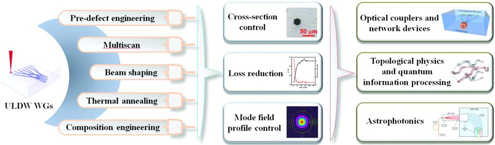
Integrated photonics is attracting considerable attention and has found many applications in both classical and quantum optics, fulfilling the requirements for the ever-growing complexity in modern optical experiments and big data communication. Femtosecond (fs) laser direct writing (FLDW) is an acknowledged technique for producing waveguides (WGs) in transparent glass that have been used to construct complex integrated photonic devices. FLDW possesses unique features, such as three-dimensional fabrication geometry, rapid prototyping, and single step fabrication, which are important for integrated communication devices and quantum photonic and astrophotonic technologies. To fully take advantage of FLDW, considerable efforts have been made to produce WGs over a large depth with low propagation loss, coupling loss, bend loss, and highly symmetrical mode field. We summarize the improved techniques as well as the mechanisms for writing high-performance WGs with controllable morphology of cross-section, highly symmetrical mode field, low loss, and high processing uniformity and efficiency, and discuss the recent progress of WGs in photonic integrated devices for communication, topological physics, quantum information processing, and astrophotonics. Prospective challenges and future research directions in this field are also pointed out.
photonic integrated circuit waveguides femtosecond laser direct writing improved techniques photonic devices Advanced Photonics
2021, 3(2): 024002
1 School of Optical and Electronic Information, Huazhong University of Science and Technology, Wuhan 430074, China
2 Department of Electro-Optics and Photonics, University of Dayton, 300 College Park, Dayton, Ohio 45469, USA
3 Advanced Photonics Center, Southeast University, Nanjing 210096, Jiangsu, China
4 School of Electronic Engineering, University of Electronic Science and Technology of China, Chengdu 611731, China
5 School of Optical-Electrical and Computer Engineering, University of Shanghai for Science and Technology, Shanghai 200093, China
Frontiers of Optoelectronics
2019, 12(1): 0188–96
1 电子科技大学光电信息学院电子薄膜与集成器件国家重点实验室, 四川 成都 610054
2 电子科技大学核心电子材料与器件协同创新中心, 四川 成都 610054
随着光网络通信容量的高速增长, 将分立的光学器件集成化以减小器件尺寸、降低成本成为光电子器件发展的必然趋势。光子集成回路具有尺寸小、功耗低、质量轻等优点, 是解决未来宽带光网络能耗大、体积大、容量小等问题的关键技术。综述了基于多项目晶圆流片的规模化光子集成技术, 主要包括硅基光子集成技术、Ⅲ-V族磷化铟集成技术, 以及以氮化硅和二氧化硅多层波导结构为基础的TriPleX集成技术; 介绍了目前可以提供这3种多项目晶圆流片光子集成技术的代工平台以及利用这些代工平台实现的一些光子集成芯片, 并对这些平台的工艺参数进行了比较。
集成光学 光子集成器件 多项目晶圆流片 光子集成回路 硅基光电子学 磷化铟 激光与光电子学进展
2017, 54(5): 050001
1 华中科技大学光学与电子信息学院光电国家实验室, 湖北 武汉 430074
2 光迅科技股份有限公司, 湖北 武汉 430074
3 中国科学技术大学先进技术研究院, 安徽 合肥 230026
利用光荧光谱及X射线双晶衍射研究了纳米压印工艺对半导体外延材料的影响。利用纳米压印工艺制作了1.55 μm通信用分布反馈(DFB)半导体激光器,并对制作的器件进行了老化寿命试验。实验结果表明,采用软模版压印并不会劣化半导体外延材料的特性。制作的半导体激光器预期寿命与普通双光束曝光法制得的器件预期相当,表明纳米压印工艺制作半导体激光器是可靠的。
集成光学 纳米压印 半导体激光器 单片光子集成电路
中国科学院半导体研究所集成光电子国家重点实验室, 北京 100083
单模垂直腔面发射激光器(VCSEL)具有低功耗、小发散角、高调制带宽和易于二维集成等优点,在光互连、光存储、高速激光打印和长波通讯等方向有着很好的应用前景。调节VCSEL顶部和底部反射层的结构可以很容易地实现单纵模条件,然而要实现横向单模输出,就要同时对出射光加以横向限制。在VCSEL的顶部反射层刻蚀出二维光子晶体结构构成的光子晶体VCSEL实现了稳定的单横模激光输出。介绍了光子晶体VCSEL的基本结构、工作原理、研究进展和应用领域,并探讨了如何使光子晶体VCSEL获得更高的出光功率、控制激光偏振特性和减小发散角等问题。最后评述了光子晶体VCSEL的国内研究现状,并对未来的研究做了展望。
激光器 光子晶体 垂直腔面发射激光器 单模 光子集成电路 激光与光电子学进展
2012, 49(9): 090003


