
Author Affiliations
Abstract
1 College of Engineering and Applied Sciences and Collaborative Innovation Center of Advanced Microstructures, Nanjing University, Nanjing 210023, China
2 School of Physics, Nanjing University, Nanjing 210023, China
3 Department of Cardiology, Affiliated Drum Tower Hospital, Medical School of Nanjing University, Nanjing 210008, China
Systemic blood circulation is one of life activity’s most important physiological functions. Continuous noninvasive hemodynamic monitoring is essential for the management of cardiovascular status. However, it is difficult to achieve systemic hemodynamic monitoring with the daily use of current devices due to the lack of multichannel and time-synchronized operation capability over the whole body. Here, we utilize a soft microfiber Bragg grating group to monitor spatiotemporal hemodynamics by taking advantage of the high sensitivity, electromagnetic immunity, and great temporal synchronization between multiple remote sensor nodes. A continuous systemic hemodynamic measurement technique is developed using all-mechanical physiological signals, such as ballistocardiogram signals and pulse waves, to illustrate the actual mechanical process of blood circulation. Multiple hemodynamic parameters, such as systemic pulse transit time, heart rate, blood pressure, and peripheral resistance, are monitored using skin-like microfiber Bragg grating patches conformally attached at different body locations. Relying on the soft microfiber Bragg grating group, the spatiotemporal hemodynamic monitoring technique opens up new possibilities in clinical medical diagnosis and daily health management.
spatiotemporal hemodynamic monitor skin-like photonic devices microfiber Bragg grating Opto-Electronic Advances
2023, 6(11): 230018
北京航空航天大学仪器科学与光电工程学院,北京 100191
随着光子材料和光子器件在可穿戴技术、智慧医疗、仿生机器人等新兴应用领域的不断拓展,研制具有优异机械柔韧性、生物相容性甚至生物可降解性的光子器件日益重要。为同时实现优异的光学性能和生物力学性能,柔性光子器件从材料合成、结构设计、功能实现到工艺制备等诸多方面亟需探索。其中,有机聚合物因其质地轻柔、生物相容性好、合成可控、结构功能易于改性等优势,被认为是制备柔性光子器件最具竞争力的材料之一。一系列新型的功能性有机光子器件,如光波导、衍射光栅、光子晶体等被相继被报道。本文综述了近年来柔性有机聚合物光子器件的研究进展,总结和分析了现有技术、方法和应用,并对未来的挑战和前景进行了讨论和展望。
激光与光电子学进展
2023, 60(13): 1316002
红外与激光工程
2022, 51(3): 20220152
1 西湖大学工学院,浙江省3D微纳加工和表征研究重点实验室,杭州 310024
2 浙江西湖高等研究院前沿技术研究所,杭州 310024
3 浙江大学信息与电子工程学院,杭州 310027
硫系玻璃由于具有较高的折射率、宽的红外波段透明窗口、较低的非线性损耗和较快的非线性响应,在光学器件领域具有巨大的应用潜力。随着近年来微纳器件加工技术的进步,基于硫系玻璃制备的新型微纳光子器件,在通信、安全、医疗、环境等领域得到了广泛的应用。本工作从硫系玻璃的物理光学性质出发,就硫系玻璃的薄膜制备工艺、微纳器件加工方法、光学器件应用及发展前景分别展开论述。
硫系玻璃 微纳光子器件 集成光学 中红外传感 相变材料 柔性光子 chalcogenide glasses micro/nano photonic devices integrated photonics mid-infrared sensing phase change materials flexible photonics
1 中国科学院 西安光学精密机械研究所 瞬态光学与光子技术国家重点实验室,陕西 西安 710119
2 中国科学院大学,北京 100049
3 华南理工大学 广东省半导体照明与信息化工程技术研究中心,广东 广州 510641
4 西北工业大学 电子信息学院 光学影像分析与学习中心,陕西 西安 710072
硫化锌(ZnS)晶体是重要的宽光谱红外窗口材料,高深径比纳米孔的超快激光制造技术为中红外波导傅立叶变换光谱仪等光子器件的实现提供了重要的技术途径。本文采用中心波长为1030 nm、重复频率为100 kHz、脉冲宽度为223 fs~20 ps可调的Yb: KGW激光光源,用石英锥镜产生高斯-贝塞尔光束,并用4f系统构建了40倍缩束的超快激光直写系统。在能量为36~63 μJ,脉宽为12.5~20 ps的情况下,在ZnS晶体上成功刻写了直径为80~320 nm的纳米孔结构。通过聚焦离子束(FIB)剥蚀和扫描电子显微镜(SEM)成像确定了纳米孔隙表面形貌、直径及深度信息。研究了激光脉冲能量、脉冲宽度对纳米孔隙的影响。结果表明,在20 ps脉冲宽度、48 µJ脉冲能量的激光参数下,纳米孔隙的深度约为270 μm。
硫化锌晶体 高深径比纳米孔 光子器件 高斯-贝塞尔光束 ZnS crystal high aspect ratio nanopores photonic devices Gaussian-Bessel beam 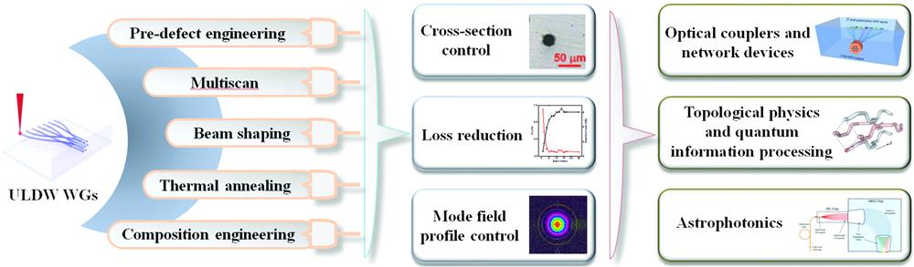
Author Affiliations
Abstract
1 Zhejiang University, College of Optical Science and Engineering, State Key Laboratory of Modern Optical Instrumentation, Hangzhou, China
2 Chinese Academy of Sciences, CAS Center for Excellence in Ultra-Intense Laser Science, Shanghai, China
Integrated photonics is attracting considerable attention and has found many applications in both classical and quantum optics, fulfilling the requirements for the ever-growing complexity in modern optical experiments and big data communication. Femtosecond (fs) laser direct writing (FLDW) is an acknowledged technique for producing waveguides (WGs) in transparent glass that have been used to construct complex integrated photonic devices. FLDW possesses unique features, such as three-dimensional fabrication geometry, rapid prototyping, and single step fabrication, which are important for integrated communication devices and quantum photonic and astrophotonic technologies. To fully take advantage of FLDW, considerable efforts have been made to produce WGs over a large depth with low propagation loss, coupling loss, bend loss, and highly symmetrical mode field. We summarize the improved techniques as well as the mechanisms for writing high-performance WGs with controllable morphology of cross-section, highly symmetrical mode field, low loss, and high processing uniformity and efficiency, and discuss the recent progress of WGs in photonic integrated devices for communication, topological physics, quantum information processing, and astrophotonics. Prospective challenges and future research directions in this field are also pointed out.
photonic integrated circuit waveguides femtosecond laser direct writing improved techniques photonic devices Advanced Photonics
2021, 3(2): 024002

Author Affiliations
Abstract
School of Physics, State Key Laboratory of Crystal Materials, Shandong University, Jinan 250100, China
Optical waveguides are far more than mere connecting elements in integrated optical systems and circuits. Benefiting from their high optical confinement and miniaturized footprints, waveguide structures established based on crystalline materials, particularly, are opening exciting possibilities and opportunities in photonic chips by facilitating their on-chip integration with different functionalities and highly compact photonic circuits. Femtosecond-laser-direct writing (FsLDW), as a true three-dimensional (3D) micromachining and microfabrication technology, allows rapid prototyping of on-demand waveguide geometries inside transparent materials via localized material modification. The success of FsLDW lies not only in its unsurpassed aptitude for realizing 3D devices but also in its remarkable material-independence that enables cross-platform solutions. This review emphasizes FsLDW fabrication of waveguide structures with 3D layouts in dielectric crystals. Their functionalities as passive and active photonic devices are also demonstrated and discussed.
femtosecond laser micromachining optical waveguide dielectric crystals photonic devices Opto-Electronic Advances
2020, 3(10): 10190042
1 北京航空航天大学 仪器科学与光电工程学院, 北京 100191
2 香港科技大学 先进显示与光电子技术国家重点实验室,香港 999077
铁电液晶因具有低电压驱动下的微秒级响应, 近年来得到科研工作者的广泛关注, 且有望应用于下一代显示及光子学器件领域。本文介绍3种典型铁电液晶光电模式, 分别为表面稳定型(surface stabilized ferroelectric liquid crystal, SSFLC)、螺旋形变型(deformed helix ferroelectric, DHF)及电致解旋型(electrically suppressed helix, ESH)。对各光电模式的工作原理及对应的电光效应进行详细阐述, 如双稳及多稳态响应、连续灰阶调制、高对比度开关等。同时, 光控取向技术在铁电液晶器件中发挥着至关重要的作用。相较于传统摩擦取向层, 光控偶氮染料取向层可实现非接触的、锚定能有效控制的铁电液晶取向, 这为铁电液晶器件的无缺陷、大面积均匀取向提供前期基础。因此, 高对比度、高分辨率、快响应的铁电液晶器件在未来的场序彩色显示、微型显示、2D/3D显示等领域有着广阔应用前景。
铁电液晶 光控取向 快响应 液晶显示 液晶光学器件 ferroelectric liquid crystal photo-alignment fast response time display photonic devices


