中国光学, 2024, 17 (1): 245, 网络出版: 2024-03-28
基于二维光子晶体全光逻辑门的设计
Design of all-optical logic gate based on two-dimensional photonic crystal
光子晶体 逻辑门 时域有限差分法 干涉 对比度 photonic crystal logic gate finite difference time domain method interference contrast
摘要
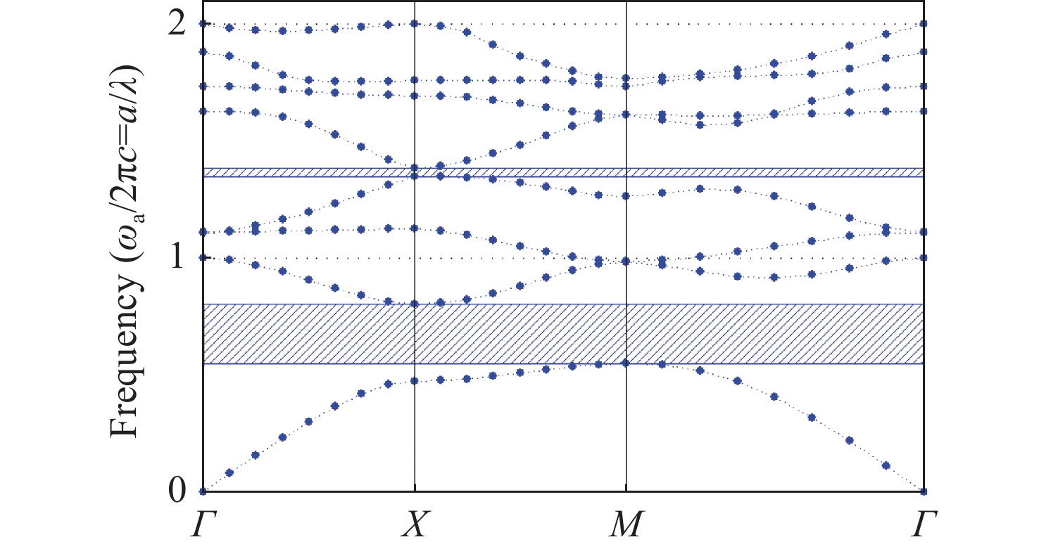
在二维光子晶体中嵌入了线缺陷,利用线性干涉效应和波导耦合,设计了一种基于二维光子晶体的同或门和与非门结构。主要采用平面波展开法对该二维光子晶体的能带结构进行分析,采用时域有限差分法,结合线性干涉效应,在Rsoft平台对所设计的同或门和与非门进行稳定电场图和归一化功率仿真。仿真结果标明:设计的同或门对比度高达29.5 dB,响应时间为0.073 ps,数据传输速率为13.7 Tbit/s;设计的与非门对比度高达24.15 dB,响应时间为0.08 ps,数据传输速率为12.5 Tbit/s。这些结果表明所设计的结构对比度高、响应时间短和数据传输速率快。
Abstract
By embedding a line defect in a two-dimensional photonic crystal and using linear interference effect and waveguide coupling, an XNOR gate and NAND gate structure based on a two-dimensional photonic crystal is designed. The band structure of the two-dimensional photonic crystal is analyzed by using the plane wave expansion method. The time-domain finite-difference method and the linear interference effect are used to simulate the stable electric field diagram and the normalized power of the XNOR gate and NAND gates on the Rsoft platform. The simulation results demonstrate that the designed XNOR gate has a contrast of 29.5 dB, a response time of 0.073 ps, and a data transmission rate of 13.7 Tbit/s. On the other hand, the designed NAND gate has a contrast of up to 24.15 dB, a response time of 0.08 ps, and a data transmission rate of 12.5 Tbit/s. It can be seen that the designed structure has a high contrast, short response time, and fast data transmission rate.
吴蓉, 张皓辰, 杨建业. 基于二维光子晶体全光逻辑门的设计[J]. 中国光学, 2024, 17(1): 245. Rong WU, Hao-chen ZHANG, Jian-ye YANG. Design of all-optical logic gate based on two-dimensional photonic crystal[J]. Chinese Optics, 2024, 17(1): 245.


