1 光场调控科学技术全国重点实验室,成都 610209
2 中国科学院空间光电精密测量技术重点实验室,成都 610209
3 中国科学院光电技术研究所,成都 610209
4 中国科学院大学 电子电气与通信工程学院,北京 100049
5 中国科学院大学 光电学院,北京 100049
为实现微弱振动信号的实时、高精度解调,提出一种基于现场可编程逻辑门阵列(FPGA)的激光多普勒微弱振动检测及信号处理方法。采用全光纤结构的光学系统,振动信号处理系统则以FPGA为核心设计。改进相位解缠模块,在增大振动测量范围的同时,使其能适用于简谐振动与复杂振动。通过模拟振动实验验证了改进后相位解缠模块,且当振幅在80 μm以内时,测量精度在5‰以内。通过对压电陶瓷实际振动目标测振实验,其频率测量误差在1 Hz以内,振幅与频率的测量精度均在1%以内。实验验证了该振动信号处理方案对于扩大振动测量范围与实现高精度目标振动解调的有效性。
激光技术 激光多普勒测振 现场可编程逻辑门阵列 信号处理 相位解缠 laser technique laser doppler vibration measurement field programmable logic gate array signal processing phase unwrapping
Author Affiliations
Abstract
1 Laboratory of Micro-Nano Optics, College of Physics and Electronic Engineering, Sichuan Normal University, Chengdu 610101, China
2 Physik-Department, Lehrstuhl für Funktionelle Materialien, Technische Universität München, James-Franck-Straße 1, 85748, Garching, Germany
3 Heinz Maier-Leibnitz Zentrum (MLZ), Technische Universität München, Lichtenbergstraße. 1, 85748, Garching, Germany
4 Tianjin Huahuixin Technology Group Co., Ltd, Zhongtian Avenue, Tianjin 300467, China
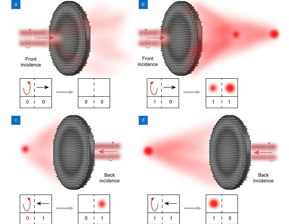
Optical logic gates play important roles in all-optical logic circuits, which lie at the heart of the next-generation optical computing technology. However, the intrinsic contradiction between compactness and robustness hinders the development in this field. Here, we propose a simple design principle that can possess multiple-input-output states according to the incident circular polarization and direction based on the metasurface doublet, which enables controlled-NOT logic gates in infrared region. Therefore, the directional asymmetric electromagnetic transmission can be achieved. As a proof of concept, a spin-dependent Janus metasurface is designed and experimentally verified that four distinct images corresponding to four input states can be captured in the far-field. In addition, since the design method is derived from geometric optics, it can be easily applied to other spectra. We believe that the proposed metasurface doublet may empower many potential applications in chiral imaging, chiroptical spectroscopy and optical computing.
metasurface polarization control asymmetric transmission logic gate Opto-Electronic Advances
2023, 6(7): 220073

Author Affiliations
Abstract
1 School of Information Science and Engineering, University of Jinan, Jinan 250022, China
2 School of Microelectronics, Shandong University, Jinan 250101, China
3 School of Integrated Circuits and Electronics, Beijing Institute of Technology, Beijing 100081, China
In the era of accelerated development in artificial intelligence as well as explosive growth of information and data throughput, underlying hardware devices that can integrate perception and memory while simultaneously offering the benefits of low power consumption and high transmission rates are particularly valuable. Neuromorphic devices inspired by the human brain are considered to be one of the most promising successors to the efficient in-sensory process. In this paper, a homojunction-based multi-functional optoelectronic synapse (MFOS) is proposed and testified. It enables a series of basic electrical synaptic plasticity, including paired-pulse facilitation/depression (PPF/PPD) and long-term promotion/depression (LTP/LTD). In addition, the synaptic behaviors induced by electrical signals could be instead achieved through optical signals, where its sensitivity to optical frequency allows the MFOS to simulate high-pass filtering applications in situ and the perception capability integrated into memory endows it with the information acquisition and processing functions as a visual system. Meanwhile, the MFOS exhibits its performances of associative learning and logic gates following the illumination with two different wavelengths. As a result, the proposed MFOS offers a solution for the realization of intelligent visual system and bionic electronic eye, and will provide more diverse application scenarios for future neuromorphic computing.
optoelectronic synapse gallium oxide filter visual system associative learning logic gate Journal of Semiconductors
2023, 44(7): 074101

Author Affiliations
Abstract
The basic indexes of all-optical integrated photonic circuits include high-density integration, ultrafast response and ultra-low energy consumption. Traditional methods mainly adopt conventional micro/nano-structures. The overall size of the circuit is large, usually reaches hundreds of microns. Besides, it is difficult to balance the ultrafast response and ultra-low energy consumption problem, and the crosstalk between two traditional devices is difficult to overcome. Here, we propose and experimentally demonstrate an approach based on inverse design method to realize a high-density, ultrafast and ultra-low energy consumption integrated photonic circuit with two all-optical switches controlling the input states of an all-optical XOR logic gate. The feature size of the whole circuit is only 2.5 μm × 7 μm, and that of a single device is 2 μm × 2 μm. The distance between two adjacent devices is as small as 1.5 μm, within wavelength magnitude scale. Theoretical response time of the circuit is 150 fs, and the threshold energy is within 10 fJ/bit. We have also considered the crosstalk problem. The circuit also realizes a function of identifying two-digit logic signal results. Our work provides a new idea for the design of ultrafast, ultra-low energy consumption all-optical devices and the implementation of high-density photonic integrated circuits.The basic indexes of all-optical integrated photonic circuits include high-density integration, ultrafast response and ultra-low energy consumption. Traditional methods mainly adopt conventional micro/nano-structures. The overall size of the circuit is large, usually reaches hundreds of microns. Besides, it is difficult to balance the ultrafast response and ultra-low energy consumption problem, and the crosstalk between two traditional devices is difficult to overcome. Here, we propose and experimentally demonstrate an approach based on inverse design method to realize a high-density, ultrafast and ultra-low energy consumption integrated photonic circuit with two all-optical switches controlling the input states of an all-optical XOR logic gate. The feature size of the whole circuit is only 2.5 μm × 7 μm, and that of a single device is 2 μm × 2 μm. The distance between two adjacent devices is as small as 1.5 μm, within wavelength magnitude scale. Theoretical response time of the circuit is 150 fs, and the threshold energy is within 10 fJ/bit. We have also considered the crosstalk problem. The circuit also realizes a function of identifying two-digit logic signal results. Our work provides a new idea for the design of ultrafast, ultra-low energy consumption all-optical devices and the implementation of high-density photonic integrated circuits.
all-optical integrated photonic circuit inverse design all-optical switch all-optical XOR logic gate Opto-Electronic Advances
2022, 5(10): 210061
光子学报
2022, 51(11): 1114005
1 北京邮电大学信息光子学与光通信国家重点实验室,北京 100876
2 国网信息通信产业集团安徽继远软件有限公司,安徽 合肥 230088
3 国网湖北省电力有限公司信息通信公司,湖北 武汉 430000
为提高光通信系统的物理层安全性能,设计并实现了一种基于双驱马赫-曾德尔调制器的加密调制一体化方案,该方案利用双驱马赫-曾德尔调制器中的矢量调制机制对明文和密钥在光域中进行异或加密操作,同时实现了加密和调制的功能复用。阐述了所提方案的基本工作原理和提升加密信号消光比的优化过程,并基于所提方案成功研制了加密调制一体化发射样机。实验结果表明,所提方案可以对传输速度为32 Gb/s的信号实现调制和加密,且信号消光比高达13.2 dB。仿真结果表明,在不同传输距离下,所提方案的接收信号消光比相比普通通断键控(OOK)系统有明显的提升。
光通信 信息安全传输 加密调制一体化 双驱马赫-曾德尔调制器 异或逻辑门加密 高消光比 光学学报
2022, 42(14): 1406001
1 长春理工大学光电工程学院,吉林 长春 130022
2 长春理工大学空间光电技术国家地方联合工程研究中心,吉林 长春 130022
3 中国科学院国家天文台长春人造卫星观测站,吉林 长春 130117
根据水下可见光通信长距离传输的需求,对水下光通信信道进行建模仿真,并设计了一种基于数字信号处理的高灵敏度水下光通信发收机。在发收机中采用现场可编程逻辑门阵列(FPGA)进行开关键控(OOK)调制、编码以及有限长单位冲激响应滤波器滤波(FIR)、自适应门限判决、滑动均值滤波等数字信号处理手段提高系统信噪比及误码性能,并在不同水质环境中进行水下光通信实验,对整体通信系统进行误码率分析,验证系统性能。实验结果表明,在满足误码率等于10-6条件下,接收机灵敏度可以达到-38 dBm。实验证明该通信系统在码速率5 Mbps、误码率10-6条件下在Ⅰ类水质中传输距离达到20 m,Ⅱ类水质中传输距离10 m,Ⅲ类水质中传输距离可以达到4.5 m。
光通信 水下可见光通信 开关键控调制 数字信号处理 现场可编程逻辑门阵列
由于贝尔态测量是量子信息处理的前提,因此提出了一种针对贝尔态的非破坏性测量方案。在该方案中,将奇偶校验门作为关键器件,利用奇偶校验门不改变输入光子状态的特性实现了C-NOT门和Toffoli门。然后,将Toffoli门和Hadamard门结合实现了对4种贝尔态的确定性测量。所提方案可用于双光子纠缠态测量,并可推广到三光子纠缠态的应用场景中,为贝尔态测量与量子信息处理提供了新的思路。
量子光学 量子信息与处理 贝尔态测量 奇偶校验门 量子逻辑门 光学学报
2021, 41(20): 2027002


