基于二维光子晶体全光逻辑门的设计
1 Introduction
Photons have faster propagation speed and greater information-carrying capacity, making them increasingly favored over electricity as a form of light and with promising future applications. As a key component in optical information storage and processing, the all-optical switch has become a new device for optical communication and computing[1]. Although photonic devices are gradually replacing electronic devices in many areas, electronic devices still dominate the market[2]. One of the main reasons is the lack of practical all-optical switches and logic gates[3]. Since all-optical logic gates can enable optical devices to achieve different output results under different input conditions, they can also achieve specific logic operation functions through the interaction between light waves[4].
Photonic crystals are synthetic artificial materials formed by periodic arrangement of media with different refractive indexes. According to the dimension, photonic crystals can be divided into one-dimensional, two-dimensional, and three-dimensional photonic crystals. Compared to one-dimensional photonic crystals, two-dimensional photonic crystals have smaller limitations and a wider application range. Compared to three-dimensional photonic crystals, two-dimensional photonic crystals have a simpler structure, require a more skilled preparation process, exhibit a higher fault tolerance rate, and the finial product performance is better. Photonic crystals have two unique properties: photonic band gap and photonic localization. Photonic band gaps can make sure the light waves within a specific wavelength range transmit. Numerous optical devices with significant practical value have emerged due to the two characteristics of photonic crystals, including optical switches[5-6], optical wavelength division multiplexers[7], optical sensors[8-9], with the advantages of simple structures, low manufacturing complexity, and easy integration.
In the process of optical communication and optical computing, in order to solve the problem of low conversion efficiency and large loss of light and electricity, the all-optical network has become one of the research hotspots. All-optical logic gates, as the basis of the all-optical network, have received extensive attention from researchers[10]. In 2017, Wu R et al.[11] proposed 'NOR' and 'NOT' all-optical logic gates. The all-optical logic gate is mainly composed of four photonic crystal waveguides ports. Its compact size and quick response speed make it a highly efficient component. In 2019, Sun X W et al.[12] used linear interference principle and self-collimation effect to design all-optical logic gates such as 'XNOR', 'NOT', which possess simple structure, small size and high contrast. In 2022, Zhang et al.[13] through introducing defects in the perfect lattice and designed an all-optical half-adder structure composed of 'AND' and 'XOR'. The contrast of 'CARRY' and 'SUM' reached 8.36 dB and 15.34 dB, respectively, and the response time was 3.63 ps.
On the basis of previous work, we mainly adopt waveguide coupling and linear interference effects to design all-optical structures for 'XNOR' and 'NAND' operations based on two-dimensional photonic crystals. This expands the range of all-optical logic gates based on two-dimensional photonic crystals. The designed structure is simulated and analyzed using the Rsoft simulation platform, combined with the plane wave expansion method and the finite difference time domain method. It is found that the device size of the structure is small, the contrast is high, the response time is short, and the stability is good.
2 Theory
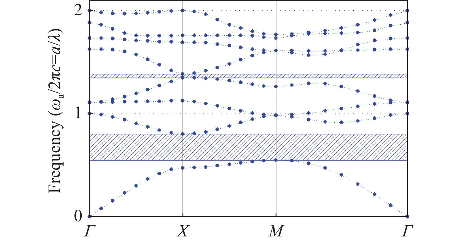
In this study, a photonic crystal with square lattice is used. The background material is air, and the circular dielectric column material is silicon. The refractive index of the dielectric column is 3.46, the lattice constant a is 0.506 μm, and the radius of the dielectric column R is 0.2 a.
To investigate the operational frequency range of the device, the plane wave expansion method is used to obtain the energy band diagram shown in Fig.1. The symbols Г, X and M in the figure represent the coordinates of the reciprocal space in the Brillouin zone. It can be seen from Fig. 1 that there are two photonic band gaps in photonic crystals only in the TE mode, and the high frequency region displays a narrow band gap. The normalized frequency is 1.336−1.3780 (ωa/2πc), with a center frequency of 1.357 (ωa/2πc). The band gap in the low frequency region is narrow, the normalized frequency is 0.549−0.800 (ωa/2πc) and the center frequency is 0.6745 (ωa/2πc). To enhance the output performance, a wavelength of 1.36−1.38 μm has been selected.
According to the waveguide theory, it is suggested that two optical signals transmitted in the same path experience phase-length and phase-cancellation interference[13]. When the transmission phase difference between two beams of optical signals is 2mπ (m = 0, 1, 2, ···), the two optical signals are superimposed on each other, resulting in phase-length interference occurs between the optical signals. This enhances the signal strength at the output end, making it stronger than any individual beam of optical signals. When the phase difference between the two optical signals equals (2m + 1) π, the two optical signals are partially cancelled, resulting in destructive interference occurs between the optical signals. Consequently, the signal strength at the output end is weaker than that of any other optical signal.
Contrast CR and response time are two crucial indicators to measure all-optical switches. Contrast CR = 10lg(T1/T0)[14-15], where T1 represents the transmittance when the output port is logically '1', and T0 represents the transmittance when the output port is logically '0'. The higher the contrast of the all-optical logic gate, the more sensitive and more stable its performance. The response time, also known as the adjustment time, is the duration required from the beginning of the output to stable output. Upon reaching the stable output, there will be a certain error, known as the error band, with a value of ±5% of the stable output value[16].
3 Design and simulation
3.1 NOR
All complex logic can be expressed in the form of simple and, or, not. This principle is fully reflected in the design process of all-optical logic gates.
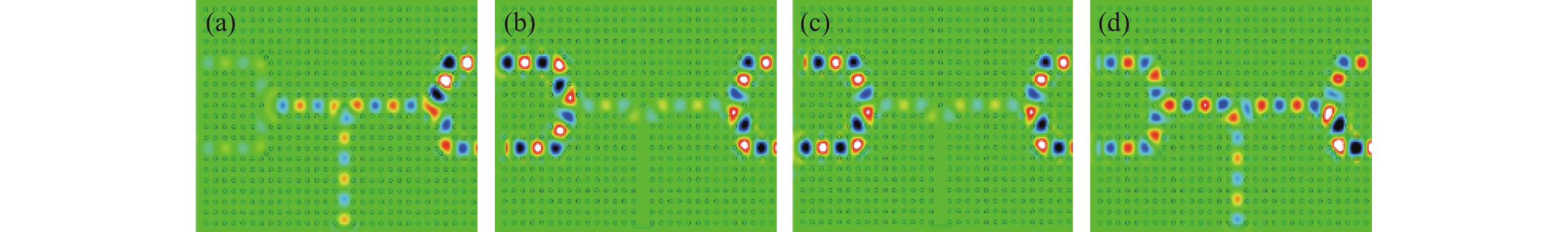
图 3.
Fig. 3. The steady-state electric field diagrams when the input is logic (a) '00', (b) '01', (c) '10' and (d) '11' respectively
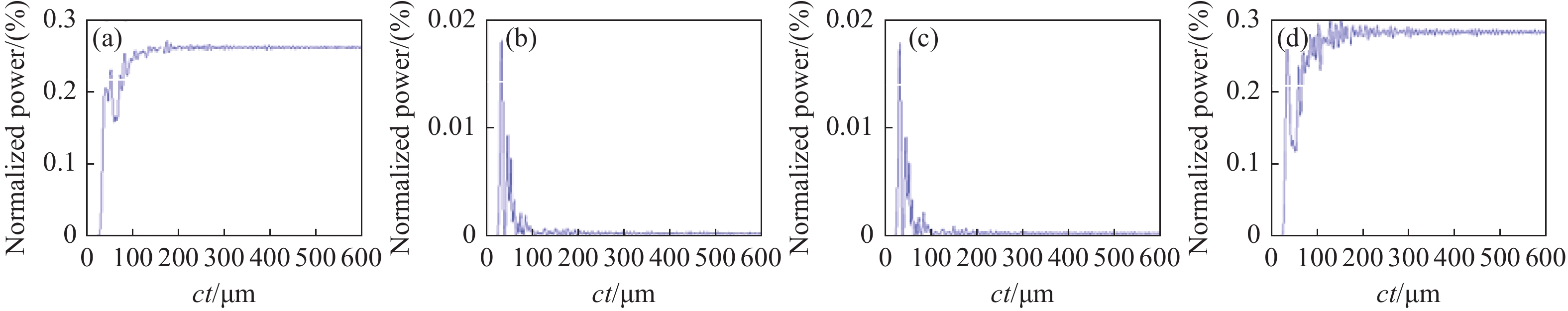
图 4.
Fig. 4. The normalized power output curves when the input is logic (a) '00', (b) '01', (c) '10' and (d) '11' respectively
It can be seen from Fig. 4 that the output power Pout changes over time until it reaches 90% of the stable power Pav at time t1. Moreover, the Fig.4 indicates that ct1 = 88 μm, the transmission speed in photon air is 3×10⁸ m/s, and t1 = 0.1468 ps. When the output power Pout reaches 10% of the stable power Pav from 0, it is denoted as time t11. Likewise, when the output power Pout reaches 90% of the stable power Pav from 10% of the stable power Pav, it is denoted as time t12. Therefore, t1 = t11+ t12. According to Fig. 4, t11 = 0.105 ps, and t12 = 0.0418 ps. Likewise, when the output power Pout reaches 90% of the stable power Pav from 10% of the stable power Pav, it is denoted as time t2. Due to the linear material used in this design, t2 = 2 t12 = 0.0836 ps. Therefore, the response period of the designed XOR gate is T = 2t12 + 2t2 = 0.1672 ps.
3.2 NAND
Through the inversion theorem transformation and NOT-logical expression,
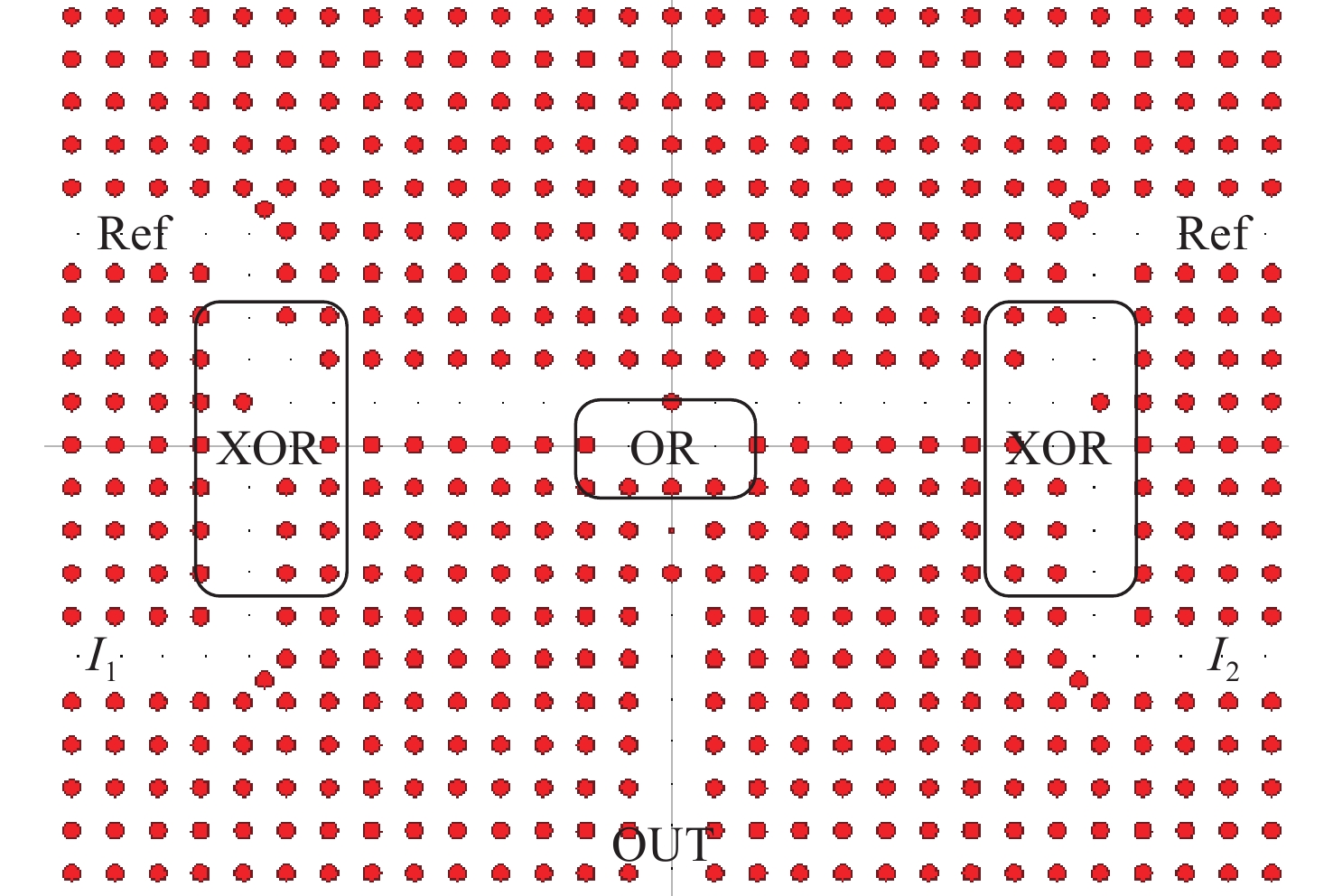
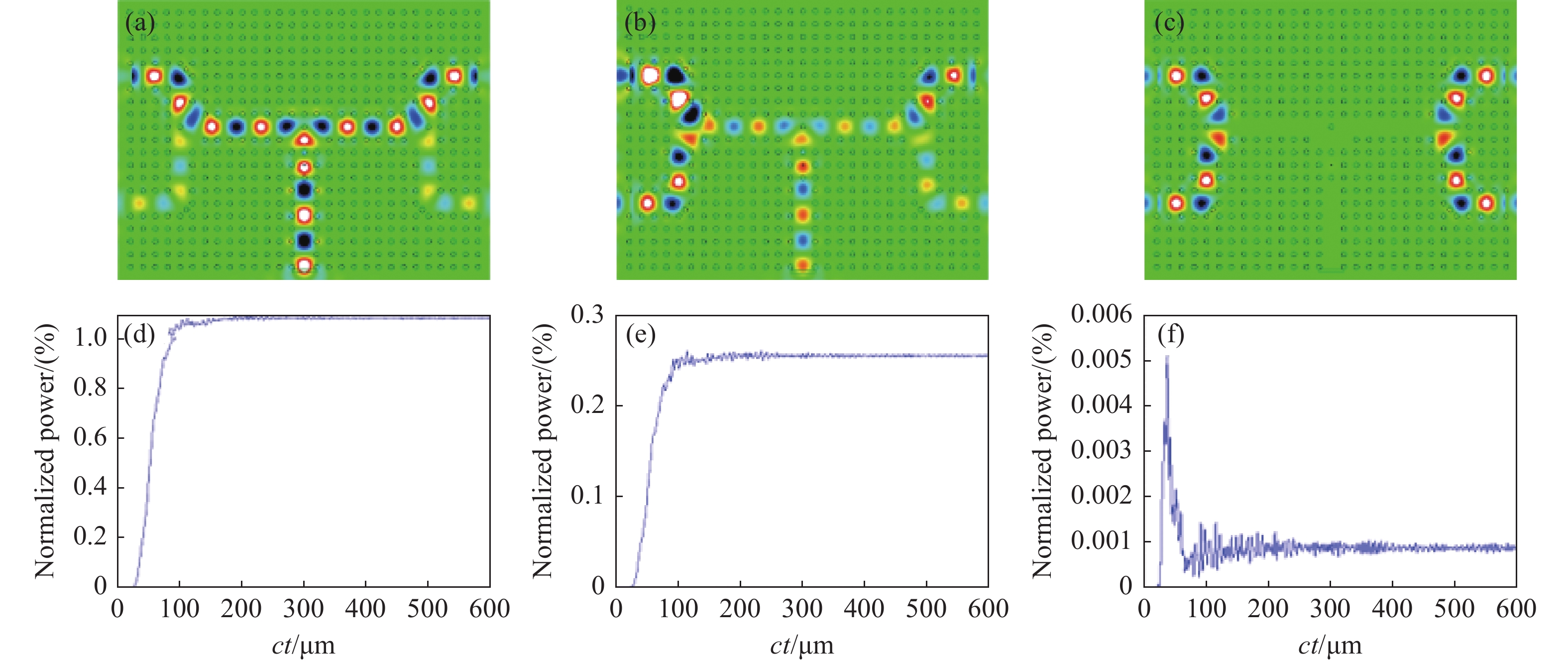
图 6.
Fig. 6. The stable electric field diagram and normalized power curve when the input logic is '00', '10' and '11', respectively. (a)-(c) are electric field diagrams when input logic is (a) '00', (b) '10', and (c) '11'; (d)-(f) are normalized curves when input logic is (d) '00', (e) '10', and (f) '00'
It can be seen from Fig. 6 that the output power Pout changes over time. The time when the output power Pout reaches 90% of the stable power Pav from 0 is denoted by t1. Further analysis of the figure represents that ct1 = 80 μm, and t1 = 0.267 ps can be calculated. The time when the output power Pout reaches 10% of the stable power Pav from 0 is denoted as t11, and the time when the output power Pout reaches 90% of the stable power Pav from 10% of the stable power Pav is denoted as t12. Therefore, t1 = t11 + t12. According to Fig. 6, it can be seen that t11 = 0.13 ps, and t12 = 0.137 ps. The time for the output power Pout to reach 10% of the stable power Pav from 90% of the stable power Pav is denoted as t2. As the design uses linear materials, t2 = 2t12 = 0.274 ps. As a result, the response period of the designed NAND gate is T = 2t12 + 2t2 =0.548 ps.
Tab. 1 Summarized features of proposed structure and previous works.
表 1. Summarized features of proposed structure and previous works
Table 1. Summarized features of proposed structure and previous works
| |||||||||||||||||
As can be seen from the table, the contrast of the output ports, both for the NOR gate and the NAND gate, have been improved considerably compared to the previous ones, which has a significant improvement in the performance of the logic device.
4 Conclusion
In a complete two-dimensional square lattice silicon photonic crystal, XOR gate and the NAND gate structures are designed by introducing line defects. The energy band structure of the photonic crystal was analyzed through plane wave expansion method. The Rsoft simulation platform was utilized to analyze the stable electric field and normalized power of the designed structure, employing the linear interference effect and the finite difference time domain method. The simulation results show that the designed same-or gate exhibits a high contrast of 29.5 dB, a response time of 0.073 ps, a response period of 0.1672 ps, and a data transmission rate of 13.7 Tbit/s. In contrast, the designed NAND gate shows a contrast of up to 24.15 dB, a response time of 0.08 ps, a response period of 0.548 ps, and a data transmission rate of 12.5 Tbit/s. These parameters show that the designed structure exhibits high contrast, a short response time and a fast data transmission rate, with potential applications in the field of integrated optics.
[2] KONG X D. Development status of electronic technology application system[J]. Electronic Technology & Software Engineering, 2017(1): 115.
[12] 孙晓雯. 基于二维光子晶体自准直效应的全光逻辑门研究[D]. 济南: 山东大学, 2018.
SUN X W. Research on alloptical logic gate based on the self collimation effect of 2D photonic crystal[D]. Ji’nan: Shong University, 2018. (in Chinese).
[13] 刘振. 基于二维光子晶体逻辑门的全光加法器研究[D]. 兰州: 兰州交通大学, 2020.
LIU ZH. Research on alloptical adder based on twodimensional photonic crystal logic gates[D]. Lanzhou: Lanzhou Jiaotong University, 2020. (in Chinese).
吴蓉, 张皓辰, 杨建业. 基于二维光子晶体全光逻辑门的设计[J]. 中国光学, 2024, 17(1): 245. Rong WU, Hao-chen ZHANG, Jian-ye YANG. Design of all-optical logic gate based on two-dimensional photonic crystal[J]. Chinese Optics, 2024, 17(1): 245.


 PDF全文
PDF全文
