Opto-Electronic Science, 2022, 1 (6): 220005, Published Online: Jul. 29, 2022   

Femtosecond laser-induced periodic structures: mechanisms, techniques, and applications Download: 987次

Author Affiliations
1 State Key Laboratory of Precision Spectroscopy, School of Physics and Materials Science, East China Normal University, Shanghai 200062, China
2 Collaborative Innovation Center of Extreme Optics, Shanxi University, Taiyuan 030006, China
3 State Key Laboratory of Optical Instrumentation, Zhejiang University, Hangzhou 310027, China
Abstract
Over the past two decades, femtosecond laser-induced periodic structures (femtosecond-LIPSs) have become ubiquitous in a variety of materials, including metals, semiconductors, dielectrics, and polymers. Femtosecond-LIPSs have become a useful laser processing method, with broad prospects in adjusting material properties such as structural color, data storage, light absorption, and luminescence. This review discusses the formation mechanism of LIPSs, specifically the LIPS formation processes based on the pump-probe imaging method. The pulse shaping of a femtosecond laser in terms of the time/frequency, polarization, and spatial distribution is an efficient method for fabricating high-quality LIPSs. Various LIPS applications are also briefly introduced. The last part of this paper discusses the LIPS formation mechanism, as well as the high-efficiency and high-quality processing of LIPSs using shaped ultrafast lasers and their applications.

1 Introduction

Femtosecond lasers have ultrashort pulse durations and high peak powers1. The interaction between femtosecond laser and matter has the advantages of minimal thermal effect and no material selectivity2, 3. Compared with nanosecond and other long-pulse lasers, femtosecond lasers could induce more regular and deeper periodic structures on different types of materials, such as metals, semiconductors, dielectrics, and polymers, without being overwhelmed by huge thermal effects4-14.

Laser-induced periodic structures (LIPSs) have been intensively studied since 1965 when Birnbaum et al. found LIPSs on the surface of germanium and gallium arsenide15, 16. Over the past two decades, ultrafast laser technology has developed rapidly. Femtosecond LIPSs (femtosecond-LIPSs) have become ubiquitous in a variety of materials, including metals, semiconductors, dielectrics, and polymers4-9, 17-31. The periods of LIPSs change significantly with the laser fluence and the number of overlapping pulses. Based on the ratio of the period (Λ) to the laser wavelength (λ), LIPSs are divided into low-spatial-frequency LIPSs (LSFLs, Λ>0.5λ) and high-spatial-frequency LIPSs (HSFLs, Λ<0.5λ)4, as shown in Fig. 1. However, the formation mechanism of femtosecond-LIPSs does not yet have a clear explanation.

Fig. 1. Scanning electron microscopy (SEM) images of (a) LSFLs on silicon8, and (b) HSFLs on ZnSe induced by 800 nm femtosecond laser. Figure reproduced with permission from: (a) ref.8, Optica Publishing Group, under the Optica Open Access Publishing Agreement; (b) ref.9, American Physical Society.

下载图片 查看所有图片

Femtosecond-LIPSs have become a useful laser processing method, with broad prospects for adjusting material properties9, 32-38 . HSFLs on the surfaces and interiors of dielectrics demonstrate birefringence effects, which have been used in data storage and waveplates34, 36, 38. LIPSs produce a significant dispersion of incident light and have been used to prepare pure and bright structural color surface32, 35. Composite structures with LIPSs can enhance light absorption and luminescence and adjust the wetting properties of a material surface33, 37, 39. The anisotropic electrical properties of LIPSs are an emerging research topic40, 41.

The main contents of this review are as follows. Section Several models of LIPS formationdiscusses the formation mechanism of LIPSs. Section Ultrafast dynamics of LIPS formation based on pump-probe imaging presents the ultrafast dynamics studied by the pump-probe imaging method. The pulse shaping of a femtosecond laser in the temporal–frequency domain, polarization, and spatial distribution is an efficient method for fabricating regular LIPSs with high efficiency, as described in Section Efficient fabrication of high-quality LIPSs with shaped ultrafast laser pulses. Section Femtosecond laser direct writing of <100 nm nanostructures introduces promising methods for laser processing nanostructures with feature sizes smaller than 100 nm. In the Section Applications of LIPSs, we briefly introduce LIPS applications in the fields of data storage, structural color surfaces, light absorption and luminescence enhancement, and the adjustment of conductive properties. The last section presents the outlook on the LIPSs. storage, structural color surfaces, light absorption and luminescence enhancement, and the adjustment of conductive properties. The last section presents the outlook on the LIPSs.

2 Several models of LIPS formation

The formation of periodic nanostructures after irradiation with a single laser beam is an interesting phenomenon. In particular, the periods of femtosecond-LIPSs change significantly with the laser fluence and the number of overlapping pulses, which renders the formation mechanism of LIPSs more complicated to determine. Numerous experimental, theoretical, and numerical studies have been performed, and several models have been proposed to explain the formation of LIPSs9, 16-18, 20, 21, 25, 42, which are described below.

2.2 Scattering light model

After irradiation with continuous and long-pulse lasers, LSFLs perpendicular or parallel to the polarization direction formed on the surfaces of semiconductor materials, where the periods were nearly equal to the laser wavelength, λ. It was proposed that these LSFLs were caused by the interference between the incident light and scattered light from the ablated surface16, 18, 43, as shown in Fig. 2. When the laser was perpendicular to the sample, period Λ was equal to laser wavelength λ. When the laser was obliquely incident at an angle θ, period Λ = λ/ (1 ± sin θ), where + and – represent the forward and backward scattered light, respectively44. This model was refined and developed by Sipe et al. They performed detailed theoretical studies and found that the generation of periodic structures depended significantly on the roughness of the material surface16. Rough structures with a height significantly smaller than the laser wavelength resulted in a periodic distribution of the laser field itself. The incident angle and polarization direction highly influenced the period and orientation of the LSFLs. This model has often been used to explain classical LSFLs induced by nanosecond or continuous wave (CW) lasers.
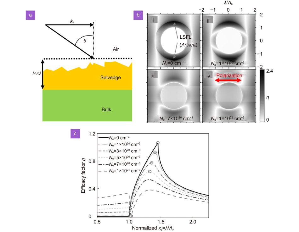
Fig. 2. (a) The schematic of light irradiated on a rough surface at an incident angle θ, where ki is the wave-vector component parallel to the surface, and l is the thickness of selvedge region. (b) The efficacy factor η as a function of the normalized LIPS wave vector for silica at different excited state. (c) The efficacy factor η along the positive ky-axis for silica at different excitation levels, with circles marking ky-positions where LIPS formation could be expected. Figure reproduced with permission from: (a) ref.16, American Physical Society; (b, c) ref.22, AIP Publishing.

下载图片 查看所有图片

Over the last two decades, scattering models have been developed and improved to explain the formation of femtosecond-LIPSs45, 46. According to the Drude model, the dielectric constants of semiconductors and dielectrics depend on the numerical density of free electrons excited by femtosecond laser. According to the Sipe model, the periodic deposition of laser energy depends on the surface roughness and dielectric constants. The formation of femtosecond-LIPSs on semiconductors and dielectrics was studied by comprehensively considering the Sipe and Drude models22, 23, 47, 48, and developed into the Sipe-Drude model22. The numerical density of free electrons and dielectric constants varied with the laser fluence, wavelength, and pulse number, which further tuned the periods of LIPSs, as shown in Fig. 2.

2.3 Surface plasmon polariton model

Under femtosecond laser irradiation, a large number of free electrons are excited, forming a plasma layer on the surface of a material. The femtosecond laser further causes the collective oscillation of the surface plasma and forms surface plasmon polaritons (SPPs), as shown in Fig. 3(a). The excitation of SPPs causes a periodic distribution of the laser field and energy deposition in the free electrons. The lattice is heated, melted, or even ablated via electron–phonon coupling, which further induces the formation of LIPSs8, 21, 25, 48, 50-62. However, in the case of vertical incidence (Fig. 3(b)), the wave vector of the SPPs is always larger than that of the incidence light. Therefore, grating structures42 or a single nanogroove25, 52 are fabricated on the sample surface in advance, and the scattered light can provide an additional wave vector, Δk, which satisfies the vector matching condition and induces SPP excitation, as shown in Fig. 3(c)21.
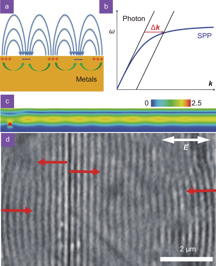
Fig. 3. (a) Schematic illustration of SPPs. (b) Dispersion curves of SPPs and light in air. (c) SPP excitation on ZnO surface in the excited state launched by a groove. (d) The SEM image of the nanostructures on the ZnO surface irradiated by 800 nm femtosecond laser, where the LSFLs originated from the nanogroove or the ablation edge, as shown as the red arrows. Figure reproduced with permission from: (b) ref.49, AIP Publishing; (c, d) ref.21, American Chemical Society.

下载图片 查看所有图片

The SPP model was used to explain the formation of LSFLs on semiconductors. The periods are expressed as follows21

Λ=λλλSPP±sin(θ),λSPP=λ×Re(ϵ+ϵdϵϵd),

where λSPP is the SPP wavelength, θ is the angle of incidence, ε is the dielectric constant of the metal, and εd is the dielectric constant of the dielectric. Under femtosecond laser irradiation, a large number of free electrons are excited, resulting in a significant change in the dielectric constant, according to the Drude model. The SPP wavelength and LSFL period can be calculated based on the dielectric constant in the excited state, which agrees well with the experimental results for semiconductors42, 51, 52. The LSFL periods induced by femtosecond laser pulses on semiconductors and metals are always smaller than the SPP wavelengths. With more laser pulse irradiation, the LSFL-assisted SPP is coupled with the laser field, forming a positive feedback effect, and leading to the formation of shorter-period LSFLs21.

2.4 Model of nanoplasmonic enhancement of laser field

The groove widths of HSFLs induced by femtosecond laser pulses are usually smaller than 100 nm, whereas the depth can reach hundreds of nanometers to micrometers. The widths of these periodically arranged nanogrooves are significantly smaller than the diffraction limit of the laser17, 20, 63-72. Figure 4(a) shows 20 nm-thick nanosheet-like nanostructures with a period of ~λ/2n in fused silica (refractive index n) induced by linearly polarized 800 nm femtosecond laser pulses. It was proposed that these nanosheets were produced by the asymmetrically localized laser-field enhancement of the nanoplasma20, as shown in Fig. 4(b).
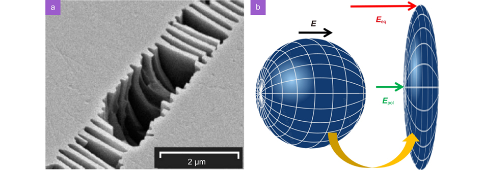
Fig. 4. (a) SEM image of HSFLs inside fused silica induced by 800 nm femtosecond laser pulses. (b) Nanoplasma growth into plane governed by local field distribution, where Epol and Eeq are the local fields on the polar axis and in the equatorial plane, respectively4, 20. Figure reproduced with permission from: (a) ref.20, American Physical Society.

下载图片 查看所有图片

The periodic distribution of the nanoplanes evolved from a random distribution of nanoplasma over many shots owing to the memory mechanism and mode selection. The period, λ0/2n, is the minimum spacing required in planar metal waveguides to support this mode with the field maxima at the metal–dielectric interface20.

Another mechanism that has been proposed for the formation of HSFLs in fused silica is photon–plasmon scattering17. By adjusting the pulse energy and cumulative pulse number of the 800 nm femtosecond laser, the HSFLs period varied from 140 to 320 nm. This phenomenon was interpreted in terms of the interference between the incident light field and the electric field of the bulk plasma wave, resulting in the periodic modulation of the electron concentration and structural changes in the fused silica17.

2.5 Other models

In recent years, several other models have been proposed to explain the formation of LIPSs, such as self-organization24, 26, 73, evanescent waves74, and Coulomb explosions75, 76. During the femtosecond laser irradiation of SiC, ZnSe, and ZnO crystals, the generation of second harmonics induces the formation of HSFLs9, 77, 78. The ripples of LSFLs on metal surfaces gradually split and evolve into HSFLs with an increase in femtosecond laser pulse irradiation79, 80.

During the femtosecond laser irradiation of semiconductor materials such as Si and ZnS, the surface plasmon layer supports two types of SPPs: those at the plasma–air interface and those at the plasma–substrate interface81. The local laser fluence and accumulated pulse number are key factors affecting the formation of LSFLs and HSFLs. Two SPP waves interfere with each other to form standing waves that induce the formation of HSFLs82, 83. A femtosecond laser was obliquely incident on a stainless steel surface and induced two periodic structures, LSFLs and HSFLs, which were caused by forward- and backward-propagating SPPs, respectively84. Numerical simulation results using the finite-difference time-domain (FDTD) method indicated that the coherent superposition of the scattering far-field (propagation) of the microstructured surface and refracted fields induced LSFLs, while the scattering near-field (evanescent) and refracted fields induced HSFLs85.

3 Ultrafast dynamics of LIPS formation based on pump-probe imaging

The phenomena of femtosecond-LIPSs are very rich, and the formation mechanisms are very complicated. Are LIPSs caused by the periodic deposition of laser energy or by self-organization during laser excitation, melting, and solidification? The propagating SPP model has been widely accepted to explain the formation of LSFLs on semiconductor and metal surfaces, however several key issues remain to be addressed. First, the SPPs on the surfaces of gold and silver are very strong86, however it is difficult to form regular LSFLs on these noble metals10. Second, the periods of the LIPSs on metal surfaces are significantly smaller than the SPP wavelengths49, 87. The further development of new methods is required to solve these problems.

Scanning electron microscopy (SEM) and atomic force microscopy (AFM) are typically used to observe LIPSs. The resolutions of these methods are very high, however they cannot be used to study the dynamics of LIPS formation. Pump-probe spectroscopy is an effective method to study the kinetics of femtosecond laser ablation88. However, transient images of LIPSs cannot be observed directly19, 79. Therefore, we developed a collinear pump-probe imaging method to study the transient processes of LIPS formation25, 49, 52, 55, 56, 89. The spatial resolution is 300 nm and the temporal resolution is 0.6 ps. To show clearly the changes in the surface microstructure, the same spot was observed at three different times: before the arrival of the pump pulse, at the designed delay time, and after the ablation spot solidified.

Figure 5 shows the optical microscope (OM) images of the transient LSFLs on the Si surface at different delay times52. The LSFL period was 680 ± 15 nm, and the direction was parallel to the nanogroove. The annular structures were caused by the diffraction effect of the concave lens. Surprisingly, periodic ripples quickly emerged. The transient ripples were clear at a delay time of 4.0 ps, which indicated that these ripples were due to surface melting, excluding other thermodynamics such as ablation and hydrodynamics. The AFM measurements further showed that the height fluctuation in the LSFL region was less than 0.6 nm, and had no spatial periodicity. The LSFL period was predicted based on the SPP model, and it coincided with the experimental results. The formation of LSFLs on silicon was due to the periodic energy deposition caused by the SPP excitation, rather than self-organization processes.

Fig. 5. OM images of silicon surface irradiated by a single 800 nm femtosecond pulse of 0.18 J/cm2.The double arrows in (a) show the laser polarization direction. Figure reproduced with permission from ref.52, Optica Publishing Group, under the Optica Open Access Publishing Agreement.

下载图片 查看所有图片

The pump-probe imaging experiments were further carried out to investigate the role of SPPs and thermal effects on the formation of LIPSs on noble-metal surfaces49. Under the irradiation of the second femtosecond laser pulse, transient periodic ripples were clearly observed on the gold film, but no obvious ripples remained after the surface solidified. The surface defects produced by the first laser pulse launched SPPs on the Au film, which caused further modulated energy deposition and induced transient LIPSs. However, because of the small electron–phonon coupling coefficient of Au, the slow heat process and strong melting effect caused the ripples to disappear. When the Au film was immersed in water, the LIPSs were retained because of the high cooling rate of the molten layers49. These experimental results indicated that the SPPs played an important role in the formation of LIPSs, while the thermal effect greatly influenced whether the transient ripples were retained after the molten surface solidified49 .

However, the period dependence of the LSFLs on metal surfaces was much different from the SPP model87, 90, 91. The SPP wavelengths were calculated by using the dielectric constants of silver, gold, copper, and aluminum in the ground states, which were significantly larger than the periods of LSFL ripples10, 49, 92. The d-band electrons in gold and silver could be excited to states above the Fermi surface93, 94. The free-electron density and plasma frequency both increased with laser fluence, resulting in longer SPP wavelengths. The LSFL periods were very different from those of the SPP model, which is a difficult problem to solve.

LSFLs are typically induced by multiple laser pulses. The material at the laser focus is partially ablated after each laser pulse irradiation, which makes the formation mechanisms more difficult to understand because of the effects of the scattered light and grating coupling feedback. Therefore, theoretical and experimental studies on the LSFLs induced by a single femtosecond laser pulse provide fundamental information on the origin of LSFLs on metal surfaces52, 95-97.
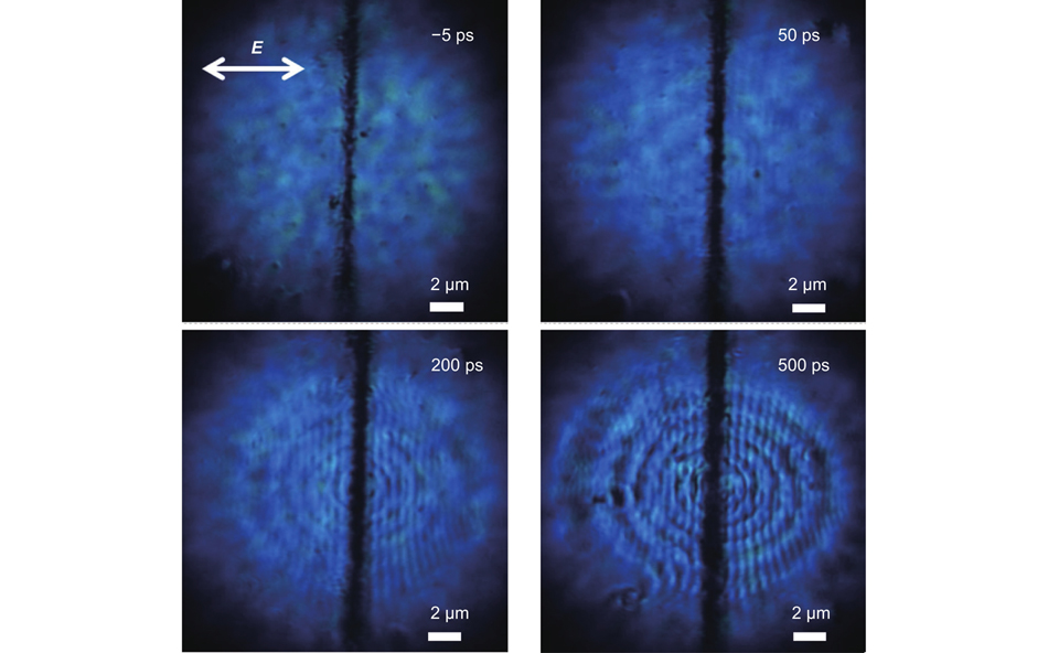
Figure 6 shows the evolution of the LSFLs formed on an Au film. The transient LSFLs began to appear at 45 ± 10 ps, and become more numerous and clearer over time25. Between 400 and 600 ps, the ripples appear to be the most distinct and regular. The ripples are perpendicular to the laser polarization with a period of 740 ± 10 nm.

Fig. 6. Evolution of LSFLs formed on Au film irradiated by a single 800 nm laser pulse with a fluence of 1.96 J/cm2. The laser polarization, E, is perpendicular to the prefabricated nanogroove. Figure reproduced with permission from ref.25, American Physical Society.
下载图片 查看所有图片

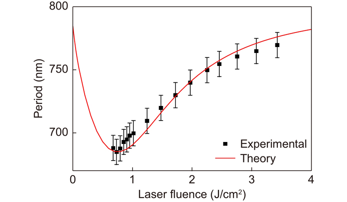
Figure 7 shows that the LSFL period increased from 685 nm to 770 nm when the fluence increased from 0.73 to 3.42 J/cm2 25, which was similar to the results for Si, GaP, and ZnO crystals51, 52, 98, 99. The SPP wavelength of gold was 780 nm for 800 nm light, which was significantly larger than the experimental value. With increasing laser fluence, free-electron density became larger, which led to longer SPP wavelength and LSFL period. Obviously, there is a great deviation between the SPP theory and the experimental results.

Fig. 7. LSFL periods as a function of laser fluence F. The black squares and error bars show the experimental data, and the red curve shows the theoretical values. Figure reproduced with permission from ref.25, American Physical Society.

下载图片 查看所有图片

The dielectric constant is a key factor affecting the SPP wavelength21, 25. The dielectric constant in the ground state was usually used to study SPP on metal surfaces, which was an important factor that caused the deviation between the SPP theory and the experimental results. Therefore, Cheng et al. proposed and studied in detail the effects of hot electron localization and d-band transitions on the dielectric constant and SPP wavelength for gold at the highly excited states during femtosecond laser irradiation25. The LSFL period calculated by the developed SPP model decreased from 780 nm to 685 nm as the fluence increased to 0.75 J/cm2. However, as F was further increased to 2.5 J/cm2, the LSFL period increased to 756 nm. The developed SPP model accorded well with the experimental results, indicating that SPP excitation was the key during the formation of LSFLs on metal surfaces.

The electronic band structures and optical properties of Ag and Ni are significantly different, and can represent noble and common metals, respectively. The dependence of the transient LSFL periods of Ag and Ni films on the laser fluence was studied using the collinear pump-probe imaging method56. The experimental results agreed well with the theoretical values based on the developed SPP theory. Thus, the developed SPP model explains the formation mechanism of LSFLs on different types of metal surfaces.

Noncollinear pump-probe imaging techniques have also been applied to observe the formation of LSFLs. Murphy et al. reported the formation of LSFLs on silicon irradiated with multiple pulses100. Using optical diffraction microscopy, Kafka et al. detected the formation of LSFLs on Cu films irradiated with a single femtosecond pulse54. Garcia-Lechuga et al. used a moving-spot multiple-pulse irradiation approach, and observed the birth and growth of individual ripples on a silicon surface101. It was demonstrated that the formation of LIPSs was initiated by free carrier generation, leading to non-thermal melting, liquid-phase overheating, and rapid solidification into the amorphous phase.

4 Efficient fabrication of high-quality LIPSs with shaped ultrafast laser pulses

4.1 Temporally shaped ultrafast laser-induced high-quality LIPSs

To efficiently fabricate uniform and regular LIPSs, three main challenges should be addressed: enhancement of periodic deposition of laser energy, reduction of residual heat, and avoidance of debris deposited on the ablation spots8. A temporally shaped ultrafast laser is an efficient tool for fabricating regular LIPSs102. By changing the sub-pulse interval, pulse number, and sub-pulse energy distribution of the burst pulse train, the regularity and uniformity of LIPSs were obviously improved, and the structural color was more vivid103, 104.

Double temporally delayed femtosecond laser beams can efficiently induce uniform LSFLs in semiconductors, metals and dielectrics105, 106. A femtosecond laser was further shaped into symmetrical three- and four-pulse sequences for the fabrication of double-grating structures and HSFLs on fused silica107.

By controlling the voltage of each element of the spatial light modulator (SLM) via computer programming, the phase and/or amplitude of the laser spectrum can be modulated, and the 4f zero-dispersion pulse-shaping system can generate shaped laser pulses with arbitrary temporal distributions8. Specifically, the number of subpulses, interval between adjacent subpulses, and pulse energy of each subpulse can be flexibly adjusted.

Regular LSFLs on silicon were processed using a 4f configuration zero-dispersion pulse-shaping system8. A Gaussian pulse is shaped into pulse trains with an interval of 16.2 ps by using periodic π-phase step modulation. The transient LIPSs started appearing on the Si surface at a delay time of 4 ps52, which was shorter than the interval between adjacent sub-pulses. Thus, the transient LIPSs have started to appear under the illumination of the two main subpulses. When the subsequent subpulse reached the sample surface, the transient LIPSs induced by the previous subpulses enhanced the excitation of the SPPs, as well as the periodic distribution of the laser field.

When the subsequent small sub-pulses reached, the surface layer remained at a very high temperature. It was further excited and partially ablated, taking away some of the remaining heat (ablative cooling effect). Moreover, the ablated plume was further excited by the subsequent subpulses, and the debris was further ionized and vaporized, resulting in fewer deposited particles. Therefore, regular and uniform LSFLs were induced on the Si surface using a shaped pulse of 16.2 ps8, as shown in Fig. 8.
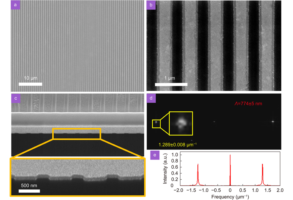
Fig. 8. (ab) SEM pictures of LSFLs induced by the shaped pulse trains with an interval of 16.2 ps. (c) The cross section of LSFLs. (d) The 2D fast Fourier transform of (b). (e) Spectra of the 2D Fourier transform along the x-axis. Figure reproduced with permission from ref.8, Optica Publishing Group, under the Optica Open Access Publishing Agreement.

下载图片 查看所有图片

The fabrication efficiency, depth, and regularity of the LSFLs when using shaped pulses of 16.2 ps were significantly better than those using Gaussian femtosecond laser pulses8. The scan velocity for fabricating regular LSFLs was 2.3 times faster, while the LSFLs depth was 2 times deeper, and the diffraction efficiency was 3 times higher than that of LSFLs using Gaussian femtosecond laser pulses.

4.2 Spatially shaped femtosecond laser-induced LIPSs with high efficiency

Arbitrary spatial intensity distribution of femtosecond laser pulses can be modulated by loading a computer-generated hologram (CGH) on a SLM, and LIPSs can be processed in parallel with high efficiency108. For example, Hayasaki et al. successfully realized the parallel processing of microstructures by loading a mixed-phase Fresnel lens on the SLM109, 110.

Maskless flexible spatial shaping based on spatiotemporal interference can modulate the interference intensity distribution into arbitrary patterns111. It was verified using a Michelson interferometer, where the phase of one laser beam was controlled via SLM.

Lin et al. developed a correction method for the spatial distortion and light intensity, which could greatly improve the accuracy of the spatial pattern and uniformity of the light intensity simply by changing the phase map loaded on the SLM112. This method was used to efficiently process colorful two-dimensional codes on silicon and shark-skin-like structures with superhydrophobic properties on stainless steel112, 113.

The laser focal point of a cylindrical lens is only a few to tens of micrometers wide, while its length is on the order of 1–10 mm114, 115. Compared with ordinary circular lenses, the efficiency of femtosecond-LIPSs can be improved by a factor of 103–104 by using cylindrical lenses, which have been demonstrated in materials such as silicon and graphene oxide11, 57, 116-118. This method is very simple, and has important implications for the industrial application of femtosecond-LIPSs in the future.

4.3 Polarization shaped femtosecond-LIPSs

By using a liquid crystal SLM and/or Q-plate, a femtosecond Gaussian laser beam could be modulated into vortex light, radially polarized or angularly polarized beam119-122, and used to directly fabricate complex LIPS patterns77, 121-129. Two laser beams with s and p polarizations were collinearly focused on the SiC surface, and nanostructures with different morphologies were fabricated by adjusting the energy ratio of these two laser beams77. Radially and angularly polarized femtosecond lasers were focused on transparent materials and HSFL patterns consistent with the polarization distribution were fabricated125.

4.4 Efficient fabrication of complex femtosecond-LIPS patterns by multi-beam interference

Multibeam interference is an efficient etching technology for processing regular periodic patterns, where the light intensity distribution in the interference field is usually imprinted on the materials. By combining laser interference technology with femtosecond-LIPSs, many complex LIPS patterns were fabricated with high efficiency and quality by simultaneously controlling the light intensity distribution and polarization distribution37, 130. Experimental and theoretical results showed that the longer-period structure was determined by the intensity distribution, whereas the LIPS pattern was determined by the polarization distribution131.

Two-beam femtosecond laser interference was used to fabricate grating structures. By changing the laser polarization direction, interesting complex periodic structures covered with LIPSs have been efficiently fabricated130, 132. Recently, large-area regular LSFLs were efficiently fabricated on a silicon wafer using double-beam femtosecond laser interference focused by cylindrical lens. The space of the double-beam interference fringes was an integer multiple of the SPP wavelength, thereby effectively exciting the resonance-enhanced SPPs. The fabricated nanogratings were very regular, uniform, and smooth, and the resolution of the diffraction light was almost the same as that with commercial gold gratings57. Using a similar method, a large area of regular and uniform LIPSs was processed on the surface of quartz glass118.

A wide variety of composite LIPSs such as hexagonally distributed nanogratings, hexagonal nanoflowers, and nanorings were efficiently fabricated on wide-bandgap SiC and ZnO semiconductors by changing the polarization combination of the three beams37, 131, as shown in Fig. 9. The four-beam interference method was further developed, and composite LIPSs such as square nanostructures, symmetric petal structures, and asymmetric helix-like structures were prepared on the surface of a ZnO crystal133.

Fig. 9. SEM images of composite LIPSs prepared by three-beam interference. The insets show the polarization combinations of the three laser beams. Figure reproduced with permission from ref.37, under a Creative Commons Attribution 4.0 International License.

下载图片 查看所有图片

5 Femtosecond laser direct writing of <100 nm nanostructures

Because of the diffraction limit, the size of the laser focus is typically a few hundred nanometers. The resolution of laser processing with high numerical aperture objectives is also on the order of hundreds of nanometers. The groove widths of HSFLs on semiconductor, dielectric, and metal surfaces induced by a femtosecond laser are typically less than 50 nm and less than 1/10 of the laser wavelength, opening up new avenues for laser processing with feature sizes smaller than 100 nm134-138. Liao et al. reported a single nanohollow channel with a width of 40 nm in porous glass using femtosecond laser-induced HSFL technology. It was used in nanofluidics in the field of single-molecule detection and biochip preparation. By precisely controlling the laser focus, fluences, and scanning speed, straight nanogrooves with widths smaller than 100 nm were prepared on the surfaces of fused silica and sapphire crystals135.

A single nanogroove with a width of 30 nm and a double-groove structure with an interval of 150 nm were fabricated on a ZnO crystal surface immersed in water by precisely controlling the 800-nm femtosecond laser fluence and scanning speed136, as shown in Fig. 10. Double-groove grating structures and single-groove grating structures with different spacings were fabricated, with groove depths ranging from 200 to 300 nm and groove widths smaller than 40 nm. Nanosquare structures with dimensions of 150 nm × 150 nm and 150 nm × 250 nm were fabricated by direct writing twice along the vertical direction.
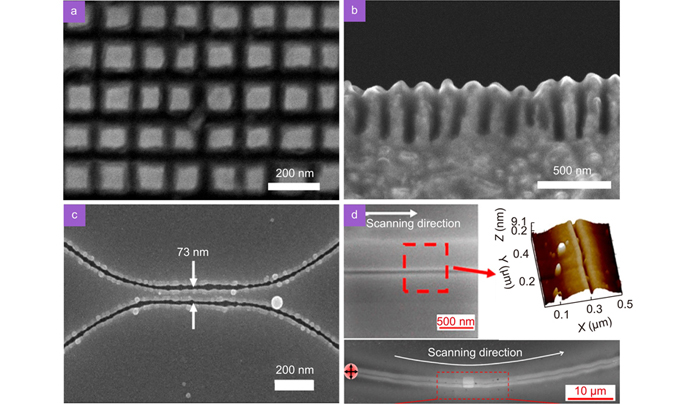
Fig. 10. (a) SEM images of nanosquares , and (b) the cross section of nanogratings . (c) Curvature and separation control of nanogrooves fabricated by 800 nm femtosecond laser with polarization control. (d) SEM and AFM images of curved single nanogroove on silicon surface induced by 800 nm femtosecond laser with orthogonally polarized dual beams. Figure reproduced with permission from: (a, b) ref.136, under Optica Open Access Publishing Agreement; (c) ref.139, under a Creative Commons Attribution 4.0 International License; (d) ref.27, American Chemical Society.

下载图片 查看所有图片

By controlling the laser polarization always perpendicular to the scanning direction, curved nanogrooves with widths smaller than 20 nm and curvature radii smaller than 100 nm were fabricated on a silicon surface139. Lin et al. processed curved nanogrooves with a feature size of 12 nm on silicon surfaces using 800 nm femtosecond laser direct writing with orthogonally polarized dual beams27.

6 Applications of LIPSs

Femtosecond-LIPSs provide a mask-free, high-efficiency processing method for tuning material properties. This method has been used in many fields, with applications that include structural colors8, 32, 35, birefringent optical components34, 36, 38, optical absorption and luminescence33, 37, 39, and electrical properties40.

6.2 Structural colors

Structural colors originate from the interference, diffraction, or scattering produced by micro/nanostructures on the surface of a material32. LIPSs have been widely used to produce structural colors on metals, semiconductors and transparent materials8, 35, 118, 140-151.

The properties of such structural colors are determined by the period, depth, and orientation of the LIPSs. LIPSs with periods in the range of 400–1500 nm were prepared on the surface of stainless steel using femtosecond lasers with different wavelengths140. These LIPSs demonstrated completely different colors under each diffraction order, such that the structural color of the stainless steel surface could cover most of the color gamut. The same LIPSs displayed different colors at different angles118, 142, 148. Therefore, surfaces with different colors were prepared by controlling the orientation of the LIPSs. Liu et al. proposed to control the orientation of LIPSs in real time using a femtosecond laser double-pulse sequence with orthogonal polarization and equal pulse energy and fabricated LIPSs with arbitrary orientations on silicon surfaces that were not affected by the scanning path147. This is of great significance for multi-layer encryption, anti-counterfeiting, and so on.

The brightness and purity of the structural colors were affected by the regularity and depth of the LIPSs. The high-efficiency preparation of high-quality LIPSs has attracted increasing attention. Zhang et al.8 fabricated very regular and deep LSFLs on a silicon surface using temporally shaped pulses via a 4f zero-dispersion system and demonstrated very bright and pure structural colors, as shown in Fig. 11. Vivid structural colors on fused silica surfaces were prepared with high efficiency using the double-beam interference of femtosecond laser focused by cylindrical lens118. Chemical etching-assisted LIPSs are also an effective method for producing bright structural colors148, 150.

Fig. 11. Structural colors of “Chinese knot” pattern made up of LSFLs fabricated by a shaped pulse of 16.2 ps on Si surface under different diffraction angles. The inset shows an SEM image of regular LSFLs. Figure reproduced with permission from ref.8, Optica Publishing Group, under the Optica Open Access Publishing Agreement.

下载图片 查看所有图片

6.3 Birefringent optical components and information storage

HSFL nanostructures inside fused silica exhibit birefringence effects comparable to those of quartz crystals34, 36, 152, 153 and have been used in the storage of multi-dimensional data, as shown in Fig. 12. Zhang et al.154 demonstrated that HSFLs could encode the intensity and polarization state of light at multiple levels and successfully retrieved digital files that were optically encrypted into five dimensions. Experiments indicated that HSFLs in silica glass have high stability and rewritability, meeting some requirements for developing high-density data storage38. Recently, Wang et al. demonstrated 100-layer 5D optical data storage based on femtosecond laser-induced birefringence with a high readout accuracy and no bit error rates155 , as shown in Fig. 12. At present, the limitations of optical storage technology lie mainly in efficient writing and fast and accurate reading. The writing speed has been increased to 225 kB/s153-155, which is mainly a result of the higher laser power and repetition frequency with pulse energy modulation, as shown in Fig. 12.
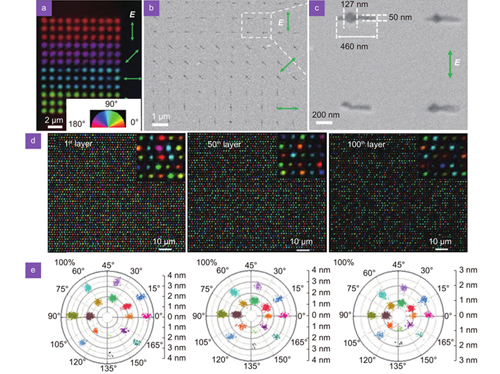
Fig. 12. (a-c) Imaging of anisotropic nanostructures and 5D optical data storage in fused silica153, 155. (a) Image of the slow axis azimuth of voxels, where the pseudo-color represents the slow axis azimuth. (b) SEM image of the nanolamella-like structure after polishing and KOH etching. (c) The enlarged area in the dashed square in (b). (d) The birefringent images of data voxels of different layers in a 100-layer 5D optical data storage in fused silica after removing the background. Insets are enlargements of small region (10 μm × 10 μm). (e) Polar diagram of the measured retardance and azimuth of all voxels in (d). Figure reproduced with permission from: (a-c) ref.153, Optica Publishing Group, under the Optica Open Access Publishing Agreement; (d, e) ref.155, under a Creative Commons Attribution License.

下载图片 查看所有图片

Mechanisms and applications based on femtosecond laser-induced birefringence have been extensively studied, including various polarization-sensitive elements70, 156-158 such as polarization beam splitters159, polarization diffraction gratings160, and polarization optical vortex rotation converters123. HSFLs fabricated in amorphous silicon161, 162, silicon carbide163 and indium tin oxide (ITO) thin films164, 165 exhibit birefringence effects two orders of magnitude higher than those of quartz glass, demonstrating that high-refractive-index materials can be used to fabricate birefringent elements. Large-area HSFLs have been efficiently fabricated on a glass surface coated with an ITO thin film using femtosecond laser direct writing focused via a cylindrical lens166. The optical retardation reached 44 nm, which was eight times that of the HSFLs processed directly on a bare glass surface.

6.4 Enhancement of optical absorption and photoluminescence

The optical properties were significantly tuned after forming complex micro-nanostructures covered with LIPSs on the surfaces of metals, semiconductors, and dielectrics33, 35, 37, 39, 118, 167-174. “Black” silicon has been extensively studied and was shown to exhibit ultra-low reflectivity and very high absorption in the UV–NIR region as a result of nanostructures fabricated by femtosecond lasers33, 39, 171, 172.

Various composite LIPSs have been efficiently fabricated on wide-bandgap SiC and ZnO semiconductors by the multi-beam interference of femtosecond lasers174, 176. These composite nanostructures exhibited greatly enhanced light absorption in the UV–NIR region, as well as an intense blue emission when excited by infrared femtosecond lasers. Compared with the smooth surface of ZnSe crystals, the blue light intensity of the composite nanostructures excited by a 1200 nm femtosecond laser was enhanced by 30–100 times175, as shown in Fig. 13.

Fig. 13. (a) SEM image of composite nanostructures on ZnSe crystal. (b) The photoluminescence (PL) spectra of the plane surface and composite nanostructures irradiated by 1200 nm femtosecond laser. Insets (i) and (ii) show PL images of the nanostructures and plane surface, respectively. Figure reproduced with permission from ref.175, AIP Publishing.

下载图片 查看所有图片

6.5 Electrical properties improved by LIPSs

Recently, the effect of LIPSs on the electrical properties of ITO40, 41, 177 and the superconducting material niobium178, 179 has received increasing attention. ITO films are widely used as transparent conductive materials in solar cells, sensors, and displays. An ITO film with LIPSs exhibited good anisotropic conductivity and, if fabricated under appropriate conditions, could even achieve unidirectional conductivity, as shown in Fig. 1441. Moreover, the transmittance in the near-infrared region was greatly enhanced40, 41, 177. These results demonstrate the potentials of femtosecond LIPSs for efficiently fabricating large-scale transparent nanowires180.
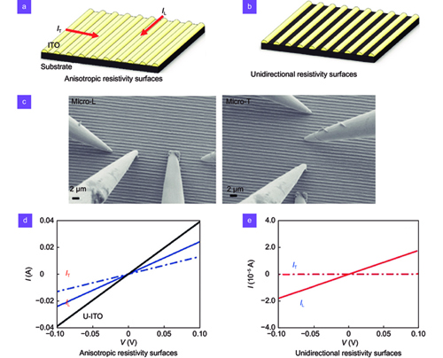
Fig. 14. (ab) Schematic illustrations of the laser-induced structure in the ITO thin film on the substrate, and the resistivity measured longitudinally (IL) or transversely (IT) along the LIPS direction. (c) Microscopic configuration of the four-point probe measurement with the probes longitudinal (Micro-L) or transverse (Micro-T) aligned with the LIPSs. (d) and (e) are the I-V curves of the anisotropic resistivity surface and the unidirectional resistivity surface measured by the Micro-L or Micro-T method, respectively. Figure reproduced with permission from ref.41, under a Creative Commons Attribution License.

下载图片 查看所有图片

Cubero et al.178, 179 analyzed the effect of laser irradiation on the critical current value of superconductors by measuring hysteresis loops, and proved that LIPSs could change the superconducting properties of niobium. The secondary electron emission from a copper surface with LIPSs was effectively reduced181, which was very effective in suppressing secondary electron emission in accelerators.

6.6 Other applications

After femtosecond laser processing, the entire ablation area is covered with nanostructures, which can effectively increase the surface roughness and reduce the contact area with the droplet. This is an efficient method to alter the hydrophilicity and hydrophobicity of sample surfaces, and has been successfully demonstrated on various materials including metals, semiconductors, dielectrics, and polymers182-192.

Femtosecond-LIPSs were optimized on steel, titanium alloy, and atomic layer deposition cemented carbide surfaces. The friction coefficient and the wear were reduced significantly, which revealed the great potential for tribological applications193-199.

7 Outlook

In this paper, the formation mechanisms, high-quality and high-efficiency processing methods, and applications of LIPSs were reviewed. We believe that the following problems that may be worth further investigation.

7.2 Formation mechanisms of LIPSs

The formation mechanism of LIPSs has always been a hot topic in this field. The scattered light model and propagating SPP model are continuously being developed and refined and have been used to explain the formation of LSFLs on dielectrics, semiconductors, and metals. However, the formation mechanism of LSFLs requires further experimental and theoretical studies, especially ultrafast dynamics.

HSFLs are typically formed after irradiation with multiple pulses. Their formation mechanism is more complex and difficult to determine than that of LSFLs, requiring extensive experimental and theoretical studies, including numerical simulations of the dynamics using the COMSOL and FDTD methods. In recent years, various far-field super-resolution imaging methods have been reported200-202. Combining the pump-probe method with far-field super-resolution imaging is very interesting and may be helpful in revealing the formation mechanism of HSFLs irradiated by a femtosecond laser.

7.3 Patterns with features of <30 nm obtained by direct writing

The groove width of HSFLs is only tens of nanometers, which provides a new method of nanofabrication using ultrafast laser direct writing. However, before this can be widely applied, there are still many problems to be solved such as the slow scanning speed and poor uniformity of the nanogrooves. In the last decade, multi-dimensional laser shaping technologies in time/frequency and polarization have been rapidly developed108, 203. Synchronizing laser direct writing and multi-dimensional laser shaping in real time will ensure that the nanogrooves grow along the direction of the direct laser writing, improve the local optical field enhancement, and reduce the residual heat of ablation. This is expected to efficiently fabricate high-quality nanopatterns with features less than 30 nm.

7.4 LIPSs based on multi-dimensional laser shaping and its applications

Large-area LIPSs fabricated with high quality, efficiency, and stability can greatly promote their applications in many fields. By developing pulse-shaping methods based on the 4f configuration zero-dispersion system or Fabry-Perot interferometer204, the regularity and depth of LIPSs can be effectively improved, which will improve the phase retardation and writing speed and reduce the bit error rate when reading out. Combining time/frequency shaping and spatial shaping can improve the regularity and depth of LIPSs fabricated with high efficiency, thereby improving the purity and brightness of the structural colors. By simultaneously controlling the polarization and spatial distribution of the laser field, nanostructures with designed patterns and specific nanogroove distributions can be processed with high efficiency. Combining time/frequency domain shaping and polarization shaping can improve the quality and efficiency of far-field nanofabrication and allow LIPS applications in new fields such as metasurfaces and microelectronics.

References

[1] Fork RL, Greene BI, Shank CVGeneration of optical pulses shorter than 0.1 psec by colliding pulse mode lockingAppl Phys Lett19813867167210.1063/1.92500

[2] Chichkov BN, Momma C, Nolte S, Von Alvensleben F, Tünnermann AFemtosecond, picosecond and nanosecond laser ablation of solidsAppl Phys A19966310911510.1007/BF01567637

[3] Sugioka K, Cheng YUltrafast lasers—reliable tools for advanced materials processingLight Sci Appl20143e14910.1038/lsa.2014.30

[4] Buividas R, Mikutis M, Juodkazis SSurface and bulk structuring of materials by ripples with long and short laser pulses: recent advancesProg Quant Electron20143811915610.1016/j.pquantelec.2014.03.002

[5] Yang QX, Liu HL, He S, Tian QY, Xu B et alCircular cladding waveguides in Pr:YAG fabricated by femtosecond laser inscription: Raman, luminescence properties and guiding performanceOpto-Electron Adv2021420000510.29026/oea.2021.200005

[6] Wang HT, Hao CL, Lin H, Wang YT, Lan T et alGeneration of super-resolved optical needle and multifocal array using graphene oxide metalensesOpto-Electron Adv20214200031

[7] Zhang YC, Jiang QL, Cao KQ, Chen TQ, Cheng K et alExtremely regular periodic surface structures in a large area efficiently induced on silicon by temporally shaped femtosecond laserPhotonics Res2021983984710.1364/PRJ.418937

[8] Jia TQ, Chen HX, Huang M, Zhao FL, Qiu JR et alFormation of nanogratings on the surface of a ZnSe crystal irradiated by femtosecond laser pulsesPhys Rev B20057212542910.1103/PhysRevB.72.125429

[9] Wang JC, Guo CLUltrafast dynamics of femtosecond laser-induced periodic surface pattern formation on metalsAppl Phys Lett20058725191410.1063/1.2146067

[10] Wang L, Chen QD, Cao XW, Buividas R, Wang XW et alPlasmonic nano-printing: large-area nanoscale energy deposition for efficient surface texturingLight Sci Appl20176e1711210.1038/lsa.2017.112

[11] Miyaji G, Miyazaki K, Zhang KF, Yoshifuji T, Fujita JMechanism of femtosecond-laser-induced periodic nanostructure formation on crystalline silicon surface immersed in waterOpt Express201220148481485610.1364/OE.20.014848

[12] Xie HB, Zhao B, Cheng JL, Chamoli SK, Zou TT et alSuper-regular femtosecond laser nanolithography based on dual-interface plasmons couplingNanophotonics2021103831384210.1515/nanoph-2021-0329

[13] Gnilitskyi I, Derrien TJY, Levy Y, Bulgakova NM, Mocek T et alHigh-speed manufacturing of highly regular femtosecond laser-induced periodic surface structures: physical origin of regularitySci Rep20177848510.1038/s41598-017-08788-z

[14] Boneberg J, Leiderer POptical near-field imaging and nanostructuring by means of laser ablationOpto-Electron Sci20221210003

[15] Birnbaum MSemiconductor surface damage produced by ruby lasersJ Appl Phys1965363688368910.1063/1.1703071

[16] Sipe JE, Young JF, Preston JS, Van Driel HMLaser-induced periodic surface structure. I. TheoryPhys Rev B1983271141115410.1103/PhysRevB.27.1141

[17] Shimotsuma Y, Kazansky PG, Qiu JR, Hirao KSelf-organized nanogratings in glass irradiated by ultrashort light pulsesPhys Rev Lett20039124740510.1103/PhysRevLett.91.247405

[18] Bonse J, Munz M, Sturm HStructure formation on the surface of indium phosphide irradiated by femtosecond laser pulsesJ Appl Phys20059701353810.1063/1.1827919

[19] Miyaji G, Miyazaki KUltrafast dynamics of periodic nanostructure formation on diamondlike carbon films irradiated with femtosecond laser pulsesAppl Phys Lett20068919190210.1063/1.2374858

[20] Bhardwaj VR, Simova E, Rajeev PP, Hnatovsky C, Taylor RS et alOptically produced arrays of planar nanostructures inside fused silicaPhys Rev Lett20069605740410.1103/PhysRevLett.96.057404

[21] Huang M, Zhao FL, Cheng Y, Xu NS, Xu ZZOrigin of laser-induced near-subwavelength ripples: interference between surface plasmons and incident laserACS Nano200934062407010.1021/nn900654v

[22] Höhm S, Rosenfeld A, Krüger J, Bonse JFemtosecond laser-induced periodic surface structures on silicaJ Appl Phys201211201490110.1063/1.4730902

[23] Bonse J, Krüger J, Höhm S, Rosenfeld AFemtosecond laser-induced periodic surface structuresJ Laser Appl20122404200610.2351/1.4712658

[24] Reif J, Varlamova O, Uhlig S, Varlamov S, Bestehorn MOn the physics of self-organized nanostructure formation upon femtosecond laser ablationAppl Phys A201411717918410.1007/s00339-014-8339-x

[25] Cheng K, Liu JK, Cao KQ, Chen L, Zhang YC et alUltrafast dynamics of single-pulse femtosecond laser-induced periodic ripples on the surface of a gold filmPhys Rev B20189818410610.1103/PhysRevB.98.184106

[26] Rudenko A, Mauclair C, Garrelie F, Stoian R, Colombier JPSelf-organization of surfaces on the nanoscale by topography-mediated selection of quasi-cylindrical and plasmonic wavesNanophotonics2019845946510.1515/nanoph-2018-0206

[27] Lin ZY, Liu HG, Ji LF, Lin WX, Hong MHRealization of ~10 nm features on semiconductor surfaces via femtosecond laser direct patterning in far field and in ambient airNano Lett2020204947495210.1021/acs.nanolett.0c01013

[28] Tsibidis GD, Fotakis C, Stratakis EFrom ripples to spikes: a hydrodynamical mechanism to interpret femtosecond laser-induced self-assembled structuresPhys Rev B201592041405(R)

[29] Vorobyev AY, Guo CLDirect femtosecond laser surface nano/microstructuring and its applicationsLaser Photonics Rev2013738540710.1002/lpor.201200017

[30] Fraggelakis F, Mincuzzi G, Lopez J, Manek-Hönninger I, Kling RControlling 2D laser nano structuring over large area with double femtosecond pulsesAppl Surf Sci201947067768610.1016/j.apsusc.2018.11.106

[31] Zhang DS, Li XZ, Fu Y, Yao QH, Li ZG et alLiquid vortexes and flows induced by femtosecond laser ablation in liquid governing formation of circular and crisscross LIPSSOpto-Electron Adv20225210066

[32] Parker AR515 million years of structural colourJ Opt A Pure Appl Opt20002R15R2810.1088/1464-4258/2/6/201

[33] Wu C, Crouch CH, Zhao L, Carey JE, Younkin R et alNear-unity below-band-gap absorption by microstructured siliconAppl Phys Lett2001781850185210.1063/1.1358846

[34] Bricchi E, Klappauf BG, Kazansky PGForm birefringence and negative index change created by femtosecond direct writing in transparent materialsOpt Lett20042911912110.1364/OL.29.000119

[35] Vorobyev AY, Guo CLColorizing metals with femtosecond laser pulsesAppl Phys Lett20089204191410.1063/1.2834902

[36] Shimotsuma Y, Sakakura M, Kazansky PG, Beresna M, Qiu JR et alUltrafast manipulation of self-assembled form birefringence in glassAdv Mater2010224039404310.1002/adma.201000921

[37] Xiong PX, Jia TQ, Jia X, Feng DH, Zhang SA et alUltraviolet luminescence enhancement of ZnO two-dimensional periodic nanostructures fabricated by the interference of three femtosecond laser beamsNew J Phys20111302304410.1088/1367-2630/13/2/023044

[38] Gu M, Li XP, Cao YYOptical storage arrays: a perspective for future big data storageLight Sci Appl20143e17710.1038/lsa.2014.58

[39] Crouch CH, Carey JE, Shen M, Mazur E, Génin FYInfrared absorption by sulfur-doped silicon formed by femtosecond laser irradiationAppl Phys A2004791635164110.1007/s00339-004-2676-0

[40] Solodar A, Cerkauskaite A, Drevinskas R, Kazansky PG, Abdulhalim IUltrafast laser induced nanostructured ITO for liquid crystal alignment and higher transparency electrodesAppl Phys Lett201811308160310.1063/1.5040692

[41] Lopez-Santos C, Puerto D, Siegel J, Macias-Montero M, Florian C et alAnisotropic resistivity surfaces produced in ITO films by laser-induced nanoscale self-organizationAdv Opt Mater20219200108610.1002/adom.202001086

[42] Garrelie F, Colombier JP, Pigeon F, Tonchev S, Faure N et alEvidence of surface plasmon resonance in ultrafast laser-induced ripplesOpt Express2011199035904310.1364/OE.19.009035

[43] Tsibidis GD, Skoulas E, Papadopoulos A, Stratakis EConvection roll-driven generation of supra-wavelength periodic surface structures on dielectrics upon irradiation with femtosecond pulsed lasersPhys Rev B201694081305(R)

[44] Emmony DC, Howson RP, Willis LJLaser mirror damage in germanium at 10.6 μmAppl Phys Lett19732359860010.1063/1.1654761

[45] Csete M, Marti O, Bor ZLaser-induced periodic surface structures on different poly-carbonate filmsAppl Phys A20017352152610.1007/s003390100973

[46] Austin DR, Kafka KRP, Lai YH, Wang Z, Zhang KK et alHigh spatial frequency laser induced periodic surface structure formation in germanium by mid-IR femtosecond pulsesJ Appl Phys201612014310310.1063/1.4964737

[47] Bonse J, Höhm S, Kirner SV, Rosenfeld A, Krüger JLaser-induced periodic surface structures-a scientific evergreenIEEE J Sel Top Quantum Electron2017239000615

[48] Bonse J, Rosenfeld A, Krüger JOn the role of surface plasmon polaritons in the formation of laser-induced periodic surface structures upon irradiation of silicon by femtosecond-laser pulsesJ Appl Phys200910610491010.1063/1.3261734

[49] Zhou K, Jia X, Jia TQ, Cheng K, Cao KQ et alThe influences of surface plasmons and thermal effects on femtosecond laser-induced subwavelength periodic ripples on Au film by pump-probe imagingJ Appl Phys201712110430110.1063/1.4978375

[50] Gurevich EL, Gurevich SVLaser induced periodic surface structures induced by surface plasmons coupled via roughnessAppl Surf Sci201430211812310.1016/j.apsusc.2013.10.141

[51] Liu JK, Jia TQ, Zhao HW, Huang YQTwo-photon excitation of surface plasmon and the period-increasing effect of low spatial frequency ripples on a GaP crystal in air/waterJ Phys D Appl Phys20164943510510.1088/0022-3727/49/43/435105

[52] Liu JK, Jia X, Wu WS, Cheng K, Feng DH et alUltrafast imaging on the formation of periodic ripples on a Si surface with a prefabricated nanogroove induced by a single femtosecond laser pulseOpt Express2018266302631510.1364/OE.26.006302

[53] Fuentes-Edfuf Y, Sánchez-Gil JA, Florian C, Giannini V, Solis J et alSurface plasmon polaritons on rough metal surfaces: role in the formation of laser-induced periodic surface structuresACS Omega201946939694610.1021/acsomega.9b00546

[54] Kafka KRP, Austin DR, Li H, Yi AY, Cheng J et alTime-resolved measurement of single pulse femtosecond laser-induced periodic surface structure formation induced by a pre-fabricated surface grooveOpt Express201523194321944110.1364/OE.23.019432

[55] Jia X, Jia TQ, Peng NN, Feng DH, Zhang SA et alDynamics of femtosecond laser-induced periodic surface structures on silicon by high spatial and temporal resolution imagingJ Appl Phys201411514310210.1063/1.4870445

[56] Cheng K, Cao KQ, Zhang YC, Han RZ, Feng DH et alUltrafast dynamics of subwavelength periodic ripples induced by single femtosecond pulse: from noble to common metalsJ Phys D Appl Phys20205328510210.1088/1361-6463/ab82d9

[57] Cao KQ, Chen L, Wu HC, Liu JK, Cheng K et alLarge-area commercial-grating-quality subwavelength periodic ripples on silicon efficiently fabricated by gentle ablation with femtosecond laser interference via two cylindrical lensesOpt Laser Technol202013110644110.1016/j.optlastec.2020.106441

[58] Derrien TJY, Itina TE, Torres R, Sarnet T, Sentis MPossible surface plasmon polariton excitation under femtosecond laser irradiation of siliconJ Appl Phys201311408310410.1063/1.4818433

[59] Tsibidis GD, Barberoglou M, Loukakos PA, Stratakis E, Fotakis CDynamics of ripple formation on silicon surfaces by ultrashort laser pulses in subablation conditionsPhys Rev B20128611531610.1103/PhysRevB.86.115316

[60] Barberoglou M, Tsibidis GD, Gray D, Magoulakis E, Fotakis C et alThe influence of ultra-fast temporal energy regulation on the morphology of Si surfaces through femtosecond double pulse laser irradiationAppl Phys A201311327328310.1007/s00339-013-7893-y

[61] Tsibidis GD, Stratakis E, Loukakos PA, Fotakis CControlled ultrashort-pulse laser-induced ripple formation on semiconductorsAppl Phys A2014114576810.1007/s00339-013-8113-5

[62] Miyaji G, Hagiya M, Miyazaki KExcitation of surface plasmon polaritons on silicon with an intense femtosecond laser pulsePhys Rev B20179604512210.1103/PhysRevB.96.045122

[63] Wortmann D, Gottmann J, Brandt N, Horn-Solle HMicro- and nanostructures inside sapphire by fs-laser irradiation and selective etchingOpt Express2008161517152210.1364/OE.16.001517

[64] Gottmann J, Wortmann D, Hörstmann-Jungemann MFabrication of sub-wavelength surface ripples and in-volume nanostructures by fs-laser induced selective etchingAppl Surf Sci20092555641564610.1016/j.apsusc.2008.10.097

[65] Richter S, Miese C, Döring S, Zimmermann F, Withford MJ et alLaser induced nanogratings beyond fused silica-periodic nanostructures in borosilicate glasses and ULE™Opt Mater Express201331161116610.1364/OME.3.001161

[66] Hnatovsky C, Taylor RS, Rajeev PP, Simova E, Bhardwaj VR et alPulse duration dependence of femtosecond-laser-fabricated nanogratings in fused silicaAppl Phys Lett20058701410410.1063/1.1991991

[67] Corbari C, Champion A, Gecevičius M, Beresna M, Bellouard Y et alFemtosecond versus picosecond laser machining of nano-gratings and micro-channels in silica glassOpt Express2013213946395810.1364/OE.21.003946

[68] Taylor RS, Hnatovsky C, Simova E, Rajeev PP, Rayner DM et alFemtosecond laser erasing and rewriting of self-organized planar nanocracks in fused silica glassOpt Lett2007322888289010.1364/OL.32.002888

[69] Juodkazis S, Nishimura K, Okuno H, Tabuchi Y, Matsuo S et alThree-dimensional laser microfabrication of metals, semiconductors, and dielectricsProc SPIE2007673267320B10.1117/12.751889

[70] Taylor R, Hnatovsky C, Simova EApplications of femtosecond laser induced self-organized planar nanocracks inside fused silica glassLaser Photonics Rev20082264610.1002/lpor.200710031

[71] Liao Y, Pan WJ, Cui Y, Qiao LL, Bellouard Y et alFormation of in-volume nanogratings with sub-100-nm periods in glass by femtosecond laser irradiationOpt Lett2015403623362610.1364/OL.40.003623

[72] Liao Y, Ni JL, Qiao LL, Huang M, Bellouard Y et alHigh-fidelity visualization of formation of volume nanogratings in porous glass by femtosecond laser irradiationOptica2015232933410.1364/OPTICA.2.000329

[73] Nayak BK, Gupta MCUltrafast laser-induced self-organized conical micro/nano surface structures and their originOpt Lasers Eng20104896697310.1016/j.optlaseng.2010.05.009

[74] Volkov SN, Kaplan AE, Miyazaki KEvanescent field at nanocorrugated dielectric surfaceAppl Phys Lett20099404110410.1063/1.3075055

[75] Dong YY, Molian PCoulomb explosion-induced formation of highly oriented nanoparticles on thin films of 3C-SiC by the femtosecond pulsed laserAppl Phys Lett200484101210.1063/1.1637948

[76] Huang M, Zhao FL, Cheng Y, Xu NS, Xu ZZMechanisms of ultrafast laser-induced deep-subwavelength gratings on graphite and diamondPhys Rev B20097912543610.1103/PhysRevB.79.125436

[77] Jia TQ, Zhao FL, Huang M, Chen HX, Qiu JR et alAlignment of nanoparticles formed on the surface of 6H-SiC crystals irradiated by two collinear femtosecond laser beamsAppl Phys Lett20068811111710.1063/1.2186067

[78] Le Harzic R, Dörr D, Sauer D, Stracke F, Zimmermann HGeneration of high spatial frequency ripples on silicon under ultrashort laser pulses irradiationAppl Phys Lett20119821190510.1063/1.3593493

[79] Hou SS, Huo YY, Xiong PX, Zhang Y, Zhang SA et alFormation of long- and short-periodic nanoripples on stainless steel irradiated by femtosecond laser pulsesJ Phys D Appl Phys20114450540110.1088/0022-3727/44/50/505401

[80] Huang M, Cheng Y, Zhao FL, Xu ZZThe significant role of plasmonic effects in femtosecond laser-induced grating fabrication on the nanoscaleAnn Phys2013525748610.1002/andp.201200136

[81] Wang L, Xu BB, Cao XW, Li QK, Tian WJ et alCompetition between subwavelength and deep-subwavelength structures ablated by ultrashort laser pulsesOptica2017463764210.1364/OPTICA.4.000637

[82] Miyazaki K, Miyaji GNanograting formation through surface plasmon fields induced by femtosecond laser pulsesJ Appl Phys201311415310810.1063/1.4826078

[83] Makin VS, Makin RS, Vorobyev AY, Guo CLDissipative nanostructures and Feigenbaum's universality in the "Metal-high-power ultrashort-pulsed polarized radiation" nonequilibrium nonlinear dynamical systemTech Phys Lett20083438739010.1134/S1063785008050088

[84] Fuentes-Edfuf Y, Sánchez-Gil JA, Garcia-Pardo M, Serna R, Tsibidis GD et alTuning the period of femtosecond laser induced surface structures in steel: from angled incidence to quill writingAppl Surf Sci201949394895510.1016/j.apsusc.2019.07.106

[85] Zhang H, Colombier JP, Li C, Faure N, Cheng GH et alCoherence in ultrafast laser-induced periodic surface structuresPhys Rev B20159217410910.1103/PhysRevB.92.174109

[86] Rahmani M, Lei DY, Giannini V, Lukiyanchuk B, Ranjbar M et alSubgroup decomposition of plasmonic resonances in hybrid oligomers: modeling the resonance lineshapeNano Lett2012122101210610.1021/nl3003683

[87] Okamuro K, Hashida M, Miyasaka Y, Ikuta Y, Tokita S et alLaser fluence dependence of periodic grating structures formed on metal surfaces under femtosecond laser pulse irradiationPhys Rev B20108216541710.1103/PhysRevB.82.165417

[88] Jia TQ, Chen HX, Huang M, Zhao FL, Li XX et alUltraviolet-infrared femtosecond laser-induced damage in fused silica and CaF2 crystalsPhys Rev B20067305410510.1103/PhysRevB.73.054105

[89] Zhou K, Jia X, Xi HX, Liu JK, Feng DH et alPeriodic surface structures on Ni-Fe film induced by a single femtosecond laser pulse with diffraction ringsChin Opt Lett20171502220110.3788/COL201715.022201

[90] Hashida M, Miyasaka Y, Ikuta Y, Tokita S, Sakabe SCrystal structures on a copper thin film with a surface of periodic self-organized nanostructures induced by femtosecond laser pulsesPhys Rev B20118323541310.1103/PhysRevB.83.235413

[91] Bashir S, Rafique MS, Nathala CS, Ajami AA, Husinsky WFemtosecond laser fluence based nanostructuring of W and Mo in ethanolPhys B2017513485710.1016/j.physb.2017.03.008

[92] Sakabe S, Hashida M, Tokita S, Namba S, Okamuro KMechanism for self-formation of periodic grating structures on a metal surface by a femtosecond laser pulsePhys Rev B200979033409

[93] Winter J, Rapp S, Schmidt M, Huber HPUltrafast laser processing of copper: a comparative study of experimental and simulated transient optical propertiesAppl Surf Sci201741721510.1016/j.apsusc.2017.02.070

[94] Chan WL, Averback RS, Cahill DGNonlinear energy absorption of femtosecond laser pulses in noble metalsAppl Phys A20099728729410.1007/s00339-009-5383-z

[95] Murphy RD, Torralva B, Adams DP, Yalisove SMLaser-induced periodic surface structure formation resulting from single-pulse ultrafast irradiation of Au microstructures on a Si substrateAppl Phys Lett201310221110110.1063/1.4807830

[96] Murphy RD, Torralva B, Adams DP, Yalisove SMPolarization dependent formation of femtosecond laser-induced periodic surface structures near stepped featuresAppl Phys Lett201410423111710.1063/1.4882998

[97] Yang M, Wu Q, Chen ZD, Zhang B, Tang BQ et alGeneration and erasure of femtosecond laser-induced periodic surface structures on nanoparticle-covered silicon by a single laser pulseOpt Lett20143934334610.1364/OL.39.000343

[98] Das SK, Messaoudi H, Debroy A, McGlynn E, Grunwald RMultiphoton excitation of surface plasmon-polaritons and scaling of nanoripple formation in large bandgap materialsOpt Mater Express201331705171510.1364/OME.3.001705

[99] Liu JK, Zhao H, Cheng K, Ju JQ, Feng DH et alUltrafast dynamics of the thin surface plasma layer and the periodic ripples formation on GaP crystal irradiated by a single femtosecond laser pulseOpt Express201927378593787610.1364/OE.27.037859

[100] Murphy RD, Torralva B, Adams DP, Yalisove SMPump-probe imaging of laser-induced periodic surface structures after ultrafast irradiation of SiAppl Phys Lett201310314110410.1063/1.4823588

[101] Garcia-Lechuga M, Puerto D, Fuentes-Edfuf Y, Solis J, Siegel JUltrafast moving-spot microscopy: birth and growth of laser-induced periodic surface structuresACS Photonics201631961196710.1021/acsphotonics.6b00514

[102] Jiang L, Wang AD, Li B, Cui TH, Lu YFElectrons dynamics control by shaping femtosecond laser pulses in micro/nanofabrication: modeling, method, measurement and applicationLight Sci Appl201871713410.1038/lsa.2017.134

[103] Guay JM, Lesina AC, Baxter J, Killaire G, Ramunno L et alTopography tuning for plasmonic color enhancement via picosecond laser burstsAdv Opt Mater20186180018910.1002/adom.201800189

[104] Giannuzzi G, Gaudiuso C, Di Franco C, Scamarcio G, Lugarà PM et alLarge area laser-induced periodic surface structures on steel by bursts of femtosecond pulses with picosecond delaysOpt Lasers Eng2019114152110.1016/j.optlaseng.2018.10.006

[105] Han WN, Jiang L, Li XW, Wang QS, Li H et alAnisotropy modulations of femtosecond laser pulse induced periodic surface structures on silicon by adjusting double pulse delayOpt Express201422158201582810.1364/OE.22.015820

[106] Zhao Z, Zhao B, Lei YH, Yang JJ, Guo CLLaser-induced regular nanostructure chains within microgrooves of Fe-based metallic glassAppl Surf Sci202052914715610.1016/j.apsusc.2020.147156

[107] Shi XS, Jiang L, Li X, Wang SM, Yuan YP et alFemtosecond laser-induced periodic structure adjustments based on electron dynamics control: from subwavelength ripples to double-grating structuresOpt Lett2013383743374610.1364/OL.38.003743

[108] Hasegawa S, Hayasaki YHolographic femtosecond laser manipulation for advanced material processingAdv Opt Technol20165395410.5937/savteh1601039M

[109] Hasegawa S, Hayasaki Y, Nishida NHolographic femtosecond laser processing with multiplexed phase fresnel lensesOpt Lett2006311705170710.1364/OL.31.001705

[110] Hasegawa S, Hayasaki YHolographic femtosecond laser processing with multiplexed phase fresnel lenses displayed on a liquid crystal spatial light modulatorOpt Rev20071420821310.1007/s10043-007-0208-9

[111] Li BH, Jiang L, Li XW, Lin ZM, Huang LL et alFlexible gray-scale surface patterning through spatiotemporal-interference-based femtosecond laser shapingAdv Opt Mater20186180102110.1002/adom.201801021

[112] Lin YH, Shi H, Jia TQDistortion and light intensity correction for spatiotemporal-interference-based spatial shapingLaser Optoelectron Prog202158031400210.3788/LOP202158.0314002

[113] Shi H, Lin YH, Jia TQ, Cao KQ, Zhang YC et alEfficient processing of super-hydrophobic biomimetic structures on stainless steel surfaces by spatiotemporal interference of two femtosecond laser beams based on spatial light modulatorActa Photon Sin2021500650110

[114] Huang J, Jiang L, Li XW, Wei QS, Wang ZP et alCylindrically focused nonablative femtosecond laser processing of long-range uniform periodic surface structures with tunable diffraction efficiencyAdv Opt Mater20197190070610.1002/adom.201900706

[115] Zou TT, Zhao B, Xin W, Wang Y, Wang B et alHigh-speed femtosecond laser plasmonic lithography and reduction of graphene oxide for anisotropic photoresponseLight Sci Appl202096910.1038/s41377-020-0311-2

[116] Dostovalov A, Bronnikov K, Korolkov V, Babin S, Mitsai E et alHierarchical anti-reflective laser-induced periodic surface structures (LIPSSs) on amorphous Si films for sensing applicationsNanoscale202012134311344110.1039/D0NR02182B

[117] Cao KQ, Chen L, Cheng K, Sun ZR, Jia TQRegular uniform large-area subwavelength nanogratings fabricated by the interference of two femtosecond laser beams via cylindrical lensChin Opt Lett20201809320110.3788/COL202018.093201

[118] Chen L, Cao KQ, Li YL, Liu JK, Zhang SA et alLarge-area straight, regular periodic surface structures produced on fused silica by the interference of two femtosecond laser beams through cylindrical lensOpto-Electron Adv2021420003610.29026/oea.2021.200036

[119] Allegre OJ, Jin Y, Perrie W, Ouyang J, Fearon E et alComplete wavefront and polarization control for ultrashort-pulse laser microprocessingOpt Express201321211982120710.1364/OE.21.021198

[120] Allegre OJ, Perrie W, Edwardson SP, Dearden G, Watkins KGLaser microprocessing of steel with radially and azimuthally polarized femtosecond vortex pulsesJ Opt20121408560110.1088/2040-8978/14/8/085601

[121] Jin Y, Allegre OJ, Perrie W, Abrams K, Ouyang J et alDynamic modulation of spatially structured polarization fields for real-time control of ultrafast laser-material interactionsOpt Express201321253332534310.1364/OE.21.025333

[122] Ouyang J, Perrie W, Allegre OJ, Heil T, Jin Y et alTailored optical vector fields for ultrashort-pulse laser induced complex surface plasmon structuringOpt Express201523125621257210.1364/OE.23.012562

[123] Beresna M, Gecevičius M, Kazansky PG, Gertus TRadially polarized optical vortex converter created by femtosecond laser nanostructuring of glassAppl Phys Lett20119820110110.1063/1.3590716

[124] Anoop KK, Rubano A, Fittipaldi R, Wang X, Paparo D et alFemtosecond laser surface structuring of silicon using optical vortex beams generated by a q-plateAppl Phys Lett2014104241604

[125] Hnatovsky C, Shvedov V, Krolikowski W, Rode ARevealing local field structure of focused ultrashort pulsesPhys Rev Lett201110612390110.1103/PhysRevLett.106.123901

[126] Lou K, Qian SX, Wang XL, Li YN, Gu B et alTwo-dimensional microstructures induced by femtosecond vector light fields on siliconOpt Express20122012012710.1364/OE.20.000120

[127] Tsibidis GD, Skoulas E, Stratakis ERipple formation on nickel irradiated with radially polarized femtosecond beamsOpt Lett2015405172517510.1364/OL.40.005172

[128] Nivas JJJ, Allahyari E, Cardano F, Rubano A, Fittipaldi R et alVector vortex beams generated by q-plates as a versatile route to direct fs laser surface structuringAppl Surf Sci20194711028103310.1016/j.apsusc.2018.12.091

[129] Nivas JJJ, He ST, Rubano A, Vecchione A, Paparo D et alDirect femtosecond laser surface structuring with optical vortex beams generated by a q-plateSci Rep201551792910.1038/srep17929

[130] Jia TQ, Baba M, Suzuki M, Ganeev RA, Kuroda H et alFabrication of two-dimensional periodic nanostructures by two-beam interference of femtosecond pulsesOpt Express2008161874187810.1364/OE.16.001874

[131] Jia X, Jia TQ, Ding LE, Xiong PX, Deng L et alComplex periodic micro/nanostructures on 6H-SiC crystal induced by the interference of three femtosecond laser beamsOpt Lett20093478879010.1364/OL.34.000788

[132] Peng NN, Huo YY, Zhou K, Jia X, Pan J et alThe development of femtosecond laser-induced periodic nanostructures and their optical propertiesActa Phys Sin20136209420110.7498/aps.62.094201

[133] Jia X, Jia TQ, Zhang SA, Sun ZR, Qiu JR et alManipulation of cross-linked micro/nanopatterns on ZnO by adjusting the femtosecond-laser polarizations of four-beam interferenceAppl Phys A20141141333133810.1007/s00339-013-7975-x

[134] Bonse J, Höhm S, Rosenfeld A, Krüger JSub-100-nm laser-induced periodic surface structures upon irradiation of titanium by Ti: sapphire femtosecond laser pulses in airAppl Phys A201311054755110.1007/s00339-012-7140-y

[135] Liao Y, Cheng Y, Liu CN, Song JX, He F et alDirect laser writing of sub-50 nm nanofluidic channels buried in glass for three-dimensional micro-nanofluidic integrationLab Chip2013131626163110.1039/c3lc41171k

[136] Liu JK, Jia TQ, Zhou K, Feng DH, Zhang SA et alDirect writing of 150 nm gratings and squares on ZnO crystal in water by using 800 nm femtosecond laserOpt Express201422323613237010.1364/OE.22.032361

[137] Huang M, Xu ZZSpontaneous scaling down of femtosecond laser-induced apertures towards the 10-nanometer level: the excitation of quasistatic surface plasmonsLaser Photonics Rev2014863365210.1002/lpor.201300212

[138] Miyaji G, Miyazaki KFabrication of 50-nm period gratings on GaN in air through plasmonic near-field ablation induced by ultraviolet femtosecond laser pulsesOpt Express2016244648465310.1364/OE.24.004648

[139] Li ZZ, Wang L, Fan H, Yu YH, Chen QD et alO-FIB: far-field-induced near-field breakdown for direct nanowriting in an atmospheric environmentLight Sci Appl202094110.1038/s41377-020-0275-2

[140] Dusser B, Sagan Z, Soder H, Faure N, Colombier JP et alControlled nanostructrures formation by ultra fast laser pulses for color markingOpt Express2010182913292410.1364/OE.18.002913

[141] Li GQ, Li JW, Yang L, Li XH, Hu YL et alEvolution of aluminum surface irradiated by femtosecond laser pulses with different pulse overlapsAppl Surf Sci201327620320910.1016/j.apsusc.2013.03.067

[142] Vorobyev AY, Guo CLSpectral and polarization responses of femtosecond laser-induced periodic surface structures on metalsJ Appl Phys200810304351310.1063/1.2842403

[143] Gräf S, Kunz C, Undisz A, Wonneberger R, Rettenmayr M et alMechano-responsive colour change of laser-induced periodic surface structuresAppl Surf Sci201947164565110.1016/j.apsusc.2018.12.051

[144] Long JY, Fan PX, Zhong ML, Zhang HJ, Xie YD et alSuperhydrophobic and colorful copper surfaces fabricated by picosecond laser induced periodic nanostructuresAppl Surf Sci201431146146710.1016/j.apsusc.2014.05.090

[145] Yao JW, Zhang CY, Liu HY, Dai QF, Wu LJ et alSelective appearance of several laser-induced periodic surface structure patterns on a metal surface using structural colors produced by femtosecond laser pulsesAppl Surf Sci20122587625763210.1016/j.apsusc.2012.04.105

[146] Li GQ, Li JW, Hu YL, Zhang CC, Li XH et alFemtosecond laser color marking stainless steel surface with different wavelengthsAppl Phys A20151181189119610.1007/s00339-014-8868-3

[147] Liu W, Jiang L, Han WN, Hu J, Li XW et alManipulation of LIPSS orientation on silicon surfaces using orthogonally polarized femtosecond laser double-pulse trainsOpt Express2019279782979310.1364/OE.27.009782

[148] Huang J, Jiang L, Li XW, Wang AD, Wang Z et alFabrication of highly homogeneous and controllable nanogratings on silicon via chemical etching-assisted femtosecond laser modificationNanophotonics2019886987810.1515/nanoph-2019-0056

[149] Zhang CY, Yao JW, Liu HY, Dai QF, Wu LJ et alColorizing silicon surface with regular nanohole arrays induced by femtosecond laser pulsesOpt Lett2012371106110810.1364/OL.37.001106

[150] Hwang JS, Park JE, Kim GW, Lee H, Yang MYFabrication of printable nanograting using solution-based laser-induced periodic surface structure processAppl Surf Sci202154714917810.1016/j.apsusc.2021.149178

[151] Gnilitskyi I, Gruzdev V, Bulgakova NM, Mocek T, Orazi LMechanisms of high-regularity periodic structuring of silicon surface by sub-MHz repetition rate ultrashort laser pulsesAppl Phys Lett201610914310110.1063/1.4963784

[152] Bricchi E, Kazansky PGExtraordinary stability of anisotropic femtosecond direct-written structures embedded in silica glassAppl Phys Lett20068811111910.1063/1.2185587

[153] Lei YH, Sakakura M, Wang L, Yu YH, Wang HJ et alHigh speed ultrafast laser anisotropic nanostructuring by energy deposition control via near-field enhancementOptica202181365137110.1364/OPTICA.433765

[154] Zhang JY, Gecevičius M, Beresna M, Kazansky PGSeemingly unlimited lifetime data storage in nanostructured glassPhys Rev Lett201411203390110.1103/PhysRevLett.112.033901

[155] Wang HJ, Lei YH, Wang L, Sakakura M, Yu YH et al100-layer error-free 5D optical data storage by ultrafast laser nanostructuring in glassLaser Photonics Rev2022162100563

[156] Beresna M, Gecevičius M, Kazansky PGPolarization sensitive elements fabricated by femtosecond laser nanostructuring of glass [Invited]Opt Mater Express2011178379510.1364/OME.1.000783

[157] Drevinskas R, Kazansky PGHigh-performance geometric phase elements in silica glassAPL Photonics2017206610410.1063/1.4984066

[158] Brasselet E, Royon A, Canioni LDense arrays of microscopic optical vortex generators from femtosecond direct laser writing of radial birefringence in glassAppl Phys Lett201210018190110.1063/1.4705414

[159] Fernandes LA, Grenier JR, Herman PR, Aitchison JS, Marques PVSFemtosecond laser fabrication of birefringent directional couplers as polarization beam splitters in fused silicaOpt Express201119119921199910.1364/OE.19.011992

[160] Beresna M, Kazansky PGPolarization diffraction grating produced by femtosecond laser nanostructuring in glassOpt Lett2010351662166410.1364/OL.35.001662

[161] Drevinskas R, Beresna M, Gecevičius M, Khenkin M, Kazanskii AG et alGiant birefringence and dichroism induced by ultrafast laser pulses in hydrogenated amorphous siliconAppl Phys Lett201510617110610.1063/1.4919538

[162] Drevinskas R, Beresna M, Zhang JY, Kazanskii AG, Kazansky PGUltrafast laser-induced metasurfaces for geometric phase manipulationAdv Opt Mater20175160057510.1002/adom.201600575

[163] Song J, Dai Y, Tao WJ, Gong M, Ma GH et alSurface birefringence of self-assembly periodic nanostructures induced on 6H-SiC surface by femtosecond laserAppl Surf Sci201636366466910.1016/j.apsusc.2015.12.096

[164] Cerkauskaite A, Drevinskas R, Solodar A, Abdulhalim I, Kazansky PGForm-birefringence in ITO thin films engineered by ultrafast laser nanostructuringACS Photonics201742944295110.1021/acsphotonics.7b01082

[165] Zhang FZ, Chen L, Zhang YC, Jiang QL, Feng DH et alHigh-performance birefringence of periodic nanostructures in FTO thin film fabricated by IR-UV femtosecond laserFront Phys20221086138910.3389/fphy.2022.861389

[166] Chen L, Cao KQ, Liu JK, Jia TQ, Li YY et alSurface birefringence of regular periodic surface structures produced on glass coated with an indium tin oxide film using a low-fluence femtosecond laser through a cylindrical lensOpt Express202028300943010610.1364/OE.402037

[167] Li H, Zhang CY, Li XF, Xiang J, Tie SL et alEnhanced upconversion luminescence from ZnO/Zn hybrid nanostructures induced on a Zn foil by femtosecond laser ablationOpt Express201523301183012610.1364/OE.23.030118

[168] Vorobyev AY, Guo CLFemtosecond laser blackening of platinumJ Appl Phys200810405351610.1063/1.2975989

[169] Vorobyev AY, Guo CLEffects of nanostructure-covered femtosecond laser-induced periodic surface structures on optical absorptance of metalsAppl Phys A20078632132410.1007/s00339-006-3800-0

[170] Vorobyev AY, Topkov AN, Gurin OV, Svich VA, Guo CLEnhanced absorption of metals over ultrabroad electromagnetic spectrumAppl Phys Lett20099512110610.1063/1.3227668

[171] Vorobyev AY, Guo CLDirect creation of black silicon using femtosecond laser pulsesAppl Surf Sci20112577291729410.1016/j.apsusc.2011.03.106

[172] Yang J, Luo FF, Kao TS, Li X, Ho GW et alDesign and fabrication of broadband ultralow reflectivity black Si surfaces by laser micro/nanoprocessingLight Sci Appl20143e18510.1038/lsa.2014.66

[173] Wang PQ, Liu Z, Xu KC, Blackwood DJ, Hong MH et alPeriodic upright nanopyramids for light management applications in ultrathin crystalline silicon solar cellsIEEE J Photovolt2017749350110.1109/JPHOTOV.2016.2641298

[174] Zhao QZ, Ciobanu F, Malzer S, Wang LJEnhancement of optical absorption and photocurrent of 6H-SiC by laser surface nanostructuringAppl Phys Lett20079112110710.1063/1.2786863

[175] Pan J, Jia TQ, Huo YY, Jia X, Feng DH et alGreat enhancement of near band-edge emission of ZnSe two-dimensional complex nanostructures fabricated by the interference of three femtosecond laser beamsJ Appl Phys201311409310210.1063/1.4820462

[176] Jia X, Jia TQ, Zhang Y, Xiong PX, Feng DH et alOptical absorption of two dimensional periodic microstructures on ZnO crystal fabricated by the interference of two femtosecond laser beamsOpt Express201018144011440810.1364/OE.18.014401

[177] Liu P, Wang WJ, Pan AF, Xiang Y, Wang DPPeriodic surface structures on the surface of indium tin oxide film obtained using picosecond laserOpt Laser Technol201810625926410.1016/j.optlastec.2018.04.019

[178] Cubero Á, Martinez E, Angurel LA, De La Fuente GF, Navarro R et alSurface superconductivity changes of niobium sheets by femtosecond laser-induced periodic nanostructuresNanomaterials202010252510.3390/nano10122525

[179] Cubero A, Martínez E, Angurel LA, De La Fuente GF, Navarro R et alEffects of laser-induced periodic surface structures on the superconducting properties of NiobiumAppl Surf Sci202050814514010.1016/j.apsusc.2019.145140

[180] Zuo P, Jiang L, Li X, Tian MY, Xu CY et alMaskless micro/nanopatterning and bipolar electrical rectification of MoS2 flakes through femtosecond laser direct writingACS Appl Mater Interfaces201911393343934110.1021/acsami.9b13059

[181] Nivas JJJ, Valadan M, Salvatore M, Fittipaldi R, Himmerlich M et alSecondary electron yield reduction by femtosecond pulse laser-induced periodic surface structuringSurf Interfaces20212510117910.1016/j.surfin.2021.101179

[182] Zorba V, Stratakis E, Barberoglou M, Spanakis E, Tzanetakis P et alBiomimetic artificial surfaces quantitatively reproduce the water repellency of a lotus leafAdv Mater2008204049405410.1002/adma.200800651

[183] Parker AR, Lawrence CRWater capture by a desert beetleNature2001414333410.1038/35102108

[184] Chen F, Zhang DS, Yang Q, Yong JL, Du GQ et alBioinspired wetting surface via laser microfabricationACS Appl Mater Interfaces201356777679210.1021/am401677z

[185] Yong JL, Yang Q, Chen F, Zhang DS, Farooq U et alA simple way to achieve superhydrophobicity, controllable water adhesion, anisotropic sliding, and anisotropic wetting based on femtosecond-laser-induced line-patterned surfacesJ Mater Chem A201425499550710.1039/C3TA14711H

[186] Zouaghi S, Six T, Bellayer S, Moradi S, Hatzikiriakos SG et alAntifouling biomimetic liquid-infused stainless steel: application to dairy industrial processingACS Appl Mater Interfaces20179265652657310.1021/acsami.7b06709

[187] Wu D, Wang JN, Wu SZ, Chen QD, Zhao S et alThree-level biomimetic rice-leaf surfaces with controllable anisotropic slidingAdv Funct Mater2011212927293210.1002/adfm.201002733

[188] Yong JL, Chen F, Li MJ, Yang Q, Fang Y et alRemarkably simple achievement of superhydrophobicity, superhydrophilicity, underwater superoleophobicity, underwater superoleophilicity, underwater superaerophobicity, and underwater superaerophilicity on femtosecond laser ablated PDMS surfacesJ Mater Chem A20175252492525710.1039/C7TA07528F

[189] Yong JL, Chen F, Yang Q, Fang Y, Huo JL et alFemtosecond laser induced hierarchical ZnO superhydrophobic surfaces with switchable wettabilityChem Commun2015519813981610.1039/C5CC02939B

[190] Moradi S, Kamal S, Englezos P, Hatzikiriakos SGFemtosecond laser irradiation of metallic surfaces: effects of laser parameters on superhydrophobicityNanotechnology20132441530210.1088/0957-4484/24/41/415302

[191] Lin Y, Han JP, Cai MY, Liu WJ, Luo X et alDurable and robust transparent superhydrophobic glass surfaces fabricated by a femtosecond laser with exceptional water repellency and thermostabilityJ Mater Chem A201869049905610.1039/C8TA01965G

[192] Moradi S, Hadjesfandiari N, Toosi SF, Kizhakkedathu JN, Hatzikiriakos SGEffect of extreme wettability on platelet adhesion on metallic implants: from superhydrophilicity to superhydrophobicityACS Appl Mater Interfaces20168176311764110.1021/acsami.6b03644

[193] Bonse J, Koter R, Hartelt M, Spaltmann D, Pentzien S et alFemtosecond laser-induced periodic surface structures on steel and titanium alloy for tribological applicationsAppl Phys A201411710311010.1007/s00339-014-8229-2

[194] Bonse J, Koter R, Hartelt M, Spaltmann D, Pentzien S et alTribological performance of femtosecond laser-induced periodic surface structures on titanium and a high toughness bearing steelAppl Surf Sci2015336212710.1016/j.apsusc.2014.08.111

[195] Wang Z, Zhao QZ, Wang CWReduction of friction of metals using laser-induced periodic surface nanostructuresMicromachines201561606161610.3390/mi6111444

[196] Bonse J, Kirner SV, Koter R, Pentzien S, Spaltmann D et alFemtosecond laser-induced periodic surface structures on titanium nitride coatings for tribological applicationsAppl Surf Sci201741857257910.1016/j.apsusc.2016.10.132

[197] Wang Z, Zhao QZFriction reduction of steel by laser-induced periodic surface nanostructures with atomic layer deposited TiO2 coatingSurf Coat Technol201834426927510.1016/j.surfcoat.2018.03.036

[198] Kunz C, Bonse J, Spaltmann D, Neumann C, Turchanin A et alTribological performance of metal-reinforced ceramic composites selectively structured with femtosecond laser-induced periodic surface structuresAppl Surf Sci202049914391710.1016/j.apsusc.2019.143917

[199] Xing YQ, Wu Z, Yang JJ, Wang XS, Liu LLIPSS combined with ALD MoS2 nano-coatings for enhancing surface friction and hydrophobic performancesSurf Coat Technol202038512539610.1016/j.surfcoat.2020.125396

[200] Lu DL, Liu ZWHyperlenses and metalenses for far-field super-resolution imagingNat Commun20123120510.1038/ncomms2176

[201] Hell SW, Sahl SJ, Bates M, Zhuang XW, Heintzmann R et alThe 2015 super-resolution microscopy roadmapJ Phys D Appl Phys20154844300110.1088/0022-3727/48/44/443001

[202] Liu YL, Chen YH, Wang F, Cai YJ, Liang CH et alRobust far-field imaging by spatial coherence engineeringOpto-Electron Adv20214210027

[203] Weiner AMUltrafast optical pulse shaping: a tutorial reviewOpt Commun20112843669369210.1016/j.optcom.2011.03.084

[204] Drever RWP, Hall JL, Kowalski FV, Hough J, Ford GM et alLaser phase and frequency stabilization using an optical resonatorAppl Phys B19833197105

Yuchan Zhang, Qilin Jiang, Mingquan Long, Ruozhong Han, Kaiqiang Cao, Shian Zhang, Donghai Feng, Tianqing Jia, Zhenrong Sun, Jianrong Qiu, Hongxing Xu. Femtosecond laser-induced periodic structures: mechanisms, techniques, and applications[J]. Opto-Electronic Science, 2022, 1(6): 220005.

本文已被 5 篇论文引用
被引统计数据来源于中国光学期刊网
引用该论文: TXT   |   EndNote

相关论文

加载中...

关于本站 Cookie 的使用提示

中国光学期刊网使用基于 cookie 的技术来更好地为您提供各项服务,点击此处了解我们的隐私策略。 如您需继续使用本网站,请您授权我们使用本地 cookie 来保存部分信息。
全站搜索
您最值得信赖的光电行业旗舰网络服务平台!