大曲率低损耗弯曲波导的飞秒激光直写【增强内容出版】
Femtosecond laser direct writing (FLDW) has been widely used in material processing to improve material performance due to its high flexibility, true three-dimensional capability, and wide applicability to various materials. Photonic integrated circuits (PICs) constructed by FLDW are advantageous in terms of high stability and strong resistance to interference, making them suitable for applications in optical interconnects, biosensing, quantum communication, and quantum simulation. With the continuous expansion and enrichment of these applications, miniaturization of photonic devices has become an inevitable trend. However, the integration density of PICs is significantly limited by the loss caused by large curvature waveguides (including 90°bending, 180° bending, and S-shaped bending) due to the low refractive index contrast of waveguides produced by single-shot FLDW. Although various methods have been reported to optimize the bending loss of large curvature waveguides, none of them can simultaneously meet the requirements of high integration density and wide applicability range. In this work, we employ a method of multiple laser modifications to enhance the refractive index contrast between the core and cladding of waveguides, optimize the cross-sectional refractive index distribution of the core, and achieve a bending loss as low as 0.64 dB/cm for S-shaped bent waveguides with a radius of 20 mm. Since the modification lines are written inside the waveguide and completely consistent with the bending shape and formation of the waveguide, this method possesses the characteristics of high integration density and wide applicability range, providing an important basis for the miniaturization of PICs.
This paper analyzes the causes of bending loss in waveguides and proposes a method of multiple laser modifications to enhance the refractive index contrast between the core and cladding of waveguides, optimizing the cross-sectional refractive index distribution of the core. Then, the mode field distribution within the bent waveguide and the bending loss of the bent waveguide before and after modification are simulated using professional optical waveguide simulation software, COMSOL and Rsoft, respectively. Finally, S-shaped bent waveguides and modification lines are written in alkaline-earth borosilicate glass using a 1030 nm femtosecond laser. By adjusting the scanning order, center spacing, writing power, angle, density, writing mode, and number of layers of both the waveguide and the modification lines, the mode conversion loss between the straight waveguide and the bent waveguide is effectively reduced, as well as the radiation loss of the bent waveguide. In addition, the central wavelength of the testing laser is set to 808 nm. After adjusting the laser to vertical polarization using a polarization controller, the laser is coupled into the waveguide through a polarization-maintaining fiber. The output light is received by a power meter after removing the scattered light using an iris filter.
In the simulation part, the bending loss of the modified bent waveguide is significantly reduced compared with the unmodified bent waveguide, as demonstrated by the comparison of bending losses before and after modification using Rsoft simulations (Fig.3). The waveguide parameters remain unchanged during the simulations. In the experimental section, cross-sectional microscope images of the bent waveguide before and after modification are compared (Fig.4), and it is observed that the dimensions of the two waveguides are similar, indicating that the added modification lines do not occupy any additional space outside the waveguide. In addition, we provide experimental and simulated mode field distributions before and after adding modification lines, and observe that after adding modification lines, the mode field of the bent waveguide is to some extent closer to the center of the waveguide. Subsequently, different writing orders for the modification lines and the waveguide are designed (Fig.5), and the minimum bending loss is achieved with the optimal writing order. Furthermore, considering the flexibility in writing the modification lines, experimental investigations are conducted on the center spacing between the modification lines and the waveguide, as well as the power of the modification lines (Fig.6), the density and angle of the modification lines (Fig.7), and the number of layers and writing mode of the modification lines (Fig.8). These parameters could alter the refractive index distribution of the bent waveguide cross section, thereby influencing the magnitude of bending loss. Therefore, by selecting appropriate parameter combinations, the bending loss can be minimized.
In this study, we employ a method of inscribing modification lines inside bent waveguides using femtosecond laser to reduce the bending loss. The power of 380 mW, the scanning speed of 40 mm/s, and the depth of 190 μm are selected as writing parameters of the waveguide. Experimental results demonstrate that at a position of 20 mm, utilizing the optimal writing order and the side-writing approach, along with the innermost modification lines positioned at a center spacing of 0.3 μm from the waveguide, a power of 300 mW, an encapsulation angle of 10°, a density of 10°, and a layer number of 2, the bending loss of the S-shaped bent waveguide could be reduced to 0.64 dB/cm. These experimental findings are consistent with the Rsoft simulation results. This method offers a more convenient and flexible option for integration in photonic chips, contributing to further improvements and advancements in their development and applications.
1 引言
飞秒激光直写(FLDW)凭借高灵活度[1-3]、真三维[4-6]以及广泛的材料适用性[7-9]等特点,被广泛应用于材料加工以改善材料性能。由FLDW构建的光子集成芯片(PIC)具有稳定性高、抗干扰能力强等优势,在光学互联[10-11]、生物传感[12-13]、量子通信[14-15]和量子模拟[16]等方面有重要应用。随着这些应用的不断丰富和拓展,光子器件小型化已成必然趋势。然而,目前飞秒激光直写的波导在小曲率半径下存在大弯曲损耗的问题[17-18],PIC的集成度受到大曲率波导弯曲(包括90
国内外已有多种优化方法被陆续报道。2013年,Arriola等[17]利用退火技术擦去由飞秒激光直写的大型多模波导的低折射率外环,提高波导芯层与包层的折射率对比度(简称波导的折射率对比度),在碱土硼硅铝酸盐玻璃中实现1550 nm波长下的单模传输和16.6 mm曲率半径下约0.37 dB/cm的弯曲损耗。2017年,Pätzold等[19]使用飞秒激光在弯曲波导外部写入多对等距的Ⅱ类轨迹(扫描轨迹处折射率降低),利用扫描轨迹产生的应力增大波导的折射率对比度,在聚甲基丙烯酸甲酯(PMMA)中实现638 nm波长下的单模传输和20 mm曲率半径下小于1 dB/cm的辐射损耗。2018年,Liu等[18]使用飞秒激光在弯曲波导外部写入一系列Ⅰ类轨迹(扫描轨迹处折射率升高)并形成“墙壁”,利用“墙壁”产生的应力增大波导的折射率对比度,在熔融石英中实现633 nm波长下的单模传输和15 mm曲率半径下约2.29 dB/cm的弯曲损耗。2021年,Lee等[20]发现使用飞秒激光在熔融石英中进行单向等距扫描可以诱导强烈的不对称应力模式并产生微裂纹。该微裂纹被用于增大弯曲波导外缘两侧的折射率对比度,实现1550 nm波长下的单模传输和10 mm曲率半径下约1 dB/cm的弯曲损耗(含传输损耗)。上述方法在降低弯曲波导的弯曲损耗方面取得了不同程度的成果,但也存在相应的问题。例如,文献[17]中的退火技术对熔融石英中的波导不起作用[21];文献[18-19]中的外部修饰方法会增大弯曲波导的体积,不利于提升PIC的集成度;文献[20]中的微裂纹只能出现在波导的某一侧,对于S型弯曲并不适用,而且这种微裂纹是否能出现在其他材料中还有待考证。因此,亟需一种集成度高且适用范围广的弯曲损耗降低方法。
本文使用比波导直写能量更低的飞秒激光修饰波导内部,通过调整波导和修饰线的扫描顺序、中心间隔以及修饰线的写入功率、角度、密度、写入方式和层数,有效降低直波导与弯曲波导之间的模式转换损耗,并减少弯曲波导的辐射损耗。此外,由于修饰线被写入波导内部,并且与波导在弯曲形状和形成方式上完全一致,因此该方法具备高度集成和广泛适用的特点,为PIC的小型化提供了重要依据。
2 基本原理和仿真验证
2.1 基本原理
波导弯曲部分的损耗可分为传输损耗、辐射损耗和模式转换损耗三部分[22]。其中,模式转换损耗是由于波导传播常数的改变所引起的;而对于曲率较大的弯曲波导,主要的辐射损耗是由于波导的弯曲使光无法完全被限制在波导中而产生的。本文讨论的弯曲损耗不包括传输损耗。
式中:
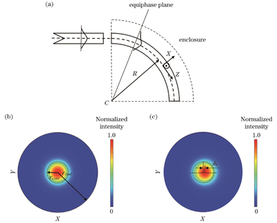
图 1. 直波导和圆弧形弯曲波导的俯视图和模拟模场分布。(a)直波导和圆弧形弯曲波导的俯视图;(b)直波导的模拟模场分布;(c)圆弧形弯曲波导的模拟模场分布
Fig. 1. Top view and simulated mode field distribution of straight waveguide and circular-arc bent waveguide. (a) Top view of straight waveguide and circular-arc bent waveguide; (b) simulated mode field distribution of straight waveguide; (c) simulated mode field distribution of circular-arc bent waveguide
式中:
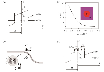
图 2. 弯曲波导在保角变换前后的折射率分布、n1-n2对
Fig. 2. Schematic diagram of refractive index distribution of bent waveguides before and after conformal transformation, influence of n1-n2 on
对于弯曲平板波导,当波导宽度远小于曲率半径(
式中:
根据上述分析,本文提出一种在弯曲波导内部写入修饰线的方法,用以减小弯曲波导的弯曲损耗。
综上所述,在弯曲波导中写入修饰线能够降低直波导与弯曲波导间的模式转换损耗以及弯曲波导的辐射损耗。
2.2 仿真验证
为进一步证明上述方法的可行性,使用Rsoft软件模拟S型弯曲波导在添加修饰线前后的横截面折射率分布和弯曲损耗
式中:
式中:
Rsoft软件模拟结果如
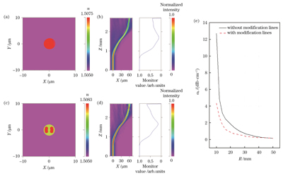
图 3. S型弯曲波导的模拟结果。(a),(b)未添加修饰线时弯曲波导的横截面折射率分布和弯曲损耗模拟图;(c),(d)添加修饰线时弯曲波导的横截面折射率分布和弯曲损耗模拟图;(e)添加和未添加修饰线时弯曲波导的弯曲损耗与曲率半径的关系
Fig. 3. Simulation results of S-shaped bent waveguide. (a),(b) Cross-sectional refractive index distribution and bending loss simulation diagrams of bent waveguide without modification lines; (c),(d) cross-sectional refractive index distribution and bending loss simulation diagrams of bent waveguide with modification lines; (e) relationship between bending loss and curvature radius of bent waveguides with and without modification lines
3 实验结果及分析
本文使用的激光器为Light Conversion公司生产的Yb∶KGW高重复频率飞秒激光器(CARBIDE,CB-5),输出激光的最大功率为5 W,中心波长为1030 nm,重复频率可调(60 kHz~1 MHz),脉宽可调(290 fs~10 ps),最大单脉冲能量83 µJ。加工样品为碱土硼铝硅酸盐玻璃(Corning Eagle XG,尺寸为25 mm×25 mm×1 mm),搭载于Aerotech公司的三维气浮平台,平台的最大运行速度、分辨率和重复定位精度分别为300 mm/s、2.5 nm和50 nm。使用空间光调制器(SLM)整形方法[31]直写具有圆形截面的波导和修饰线。测试波导的弯曲损耗时,使用中心波长为808 nm的半导体激光器产生激光。激光器输出的激光被偏振控制器调整为竖直偏振后,经保偏光纤入射到波导中;接着,波导输出的激光被虹膜滤光片滤去散射光,并由功率计接收。
本文主要的实验参数如下所述。首先,波导的直写速度和功率分别固定为40 mm/s和380 mW,且位于样品表面以下190 µm,该参数下直波导具有最小的传输损耗。其次,弯曲波导首尾直波导间的距离被固定为58.5 μm,远小于
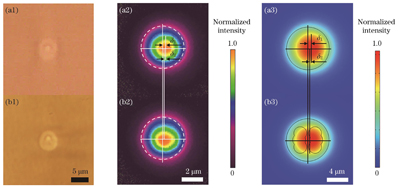
图 4. 光学显微镜照片和模场分布图片。(a1),(b1)添加修饰线前后弯曲波导的横截面光学显微镜照片;(a2),(b2)对应(a1)和(b1)的模场分布图片;(a3),(b3)添加修饰线前后弯曲波导的模拟模场分布图片
Fig. 4. Optical microscope photos and mode field distribution pictures. (a1),(b1) Cross-sectional optical microscope photos of bent waveguide before and after adding modification line, respectively; (a2),(b2) mode field distribution pictures corresponding to (a1) and (b1), respectively; (a3),(b3) simulated mode field distribution images of bent waveguide before and after adding modification line, respectively
修饰线排布紧密且被写入弯曲波导内部,因此它们的数量以及它们和波导的写入顺序都会影响弯曲波导横截面的折射率分布[32],从而改变弯曲损耗的大小。根据FLDW自深而浅的直写特性,设计了不同的写入顺序,如
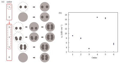
图 5. 不同的波导和修饰线写入顺序及其对应的弯曲损耗。(a)波导和修饰线的写入顺序示意图;(b)不同写入顺序下波导的弯曲损耗
Fig. 5. Different schemes of writing order of waveguide and modification lines and their corresponding bending losses. (a) Schematic diagram of writing order of waveguide and modification lines; (b) bending losses of waveguides under different writing schemes
在确定最优写入顺序之后,分别探究了各可变参数对波导弯曲损耗的影响。
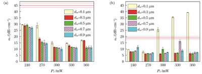
图 6. 不同
Fig. 6. Bending losses of waveguides under different
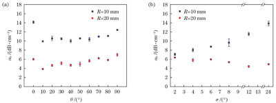
图 7. 不同
Fig. 7. Bending losses of waveguide under different
由于弯曲波导的弯曲损耗主要受其外凸侧横截面的折射率分布所影响[33],因此进一步探究了只在S型弯曲波导两段圆弧的外凸侧添加修饰线时其弯曲损耗的大小。
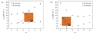
图 8. 不同修饰线写入方式、
Fig. 8. Bending losses of waveguide under different writing methods of modification lines,
4 结论
本文使用飞秒激光在弯曲波导内部写入修饰线的方法降低弯曲波导的弯曲损耗。探究了不同半径下修饰线和波导的写入顺序、中心间隔、修饰线的写入功率、写入密度、包覆角度、写入方式以及写入层数对弯曲波导损耗的影响。实验结果表明,在
[1] Ams M, Marshall G D, Spence D J, et al. Slit beam shaping method for femtosecond laser direct-write fabrication of symmetric waveguides in bulk glasses[J]. Optics Express, 2005, 13(15): 5676-5681.
[2] Ni J C, Liu S L, Chen Y, et al. Direct observation of spin-orbit interaction of light via chiroptical responses[J]. Nano Letters, 2022, 22(22): 9013-9019.
[3] Lin Z Y, Hong M H. Femtosecond laser precision engineering: from micron, submicron, to nanoscale[J]. Ultrafast Science, 2021, 2021: 9783514.
[4] 龙婧, 焦玢璋, 范旭浩, 等. 飞秒激光组装一维纳米材料及其应用[J]. 中国激光, 2021, 48(2): 0202017.
[5] Gross S, Riesen N, Love J D, et al. Three-dimensional ultra-broadband integrated tapered mode multiplexers[J]. Laser & Photonics Reviews, 2014, 8(5): L81-L85.
[6] Gross S, Withford M J. Ultrafast-laser-inscribed 3D integrated photonics: challenges and emerging applications[J]. Nanophotonics, 2015, 4(3): 332-352.
[7] 廖嘉宁, 王欣达, 周兴汶, 等. 飞秒激光直写铜微电极研究[J]. 中国激光, 2019, 46(10): 1002013.
[8] Roth G L, Kefer S, Hessler S, et al. Polymer photonic crystal waveguides generated by femtosecond laser[J]. Laser & Photonics Reviews, 2021, 15(11): 2100215.
[9] 张彬, 李子琦, 王磊, 等. 飞秒激光直写激光晶体光波导的研究进展[J]. 激光与光电子学进展, 2020, 57(11): 111415.
[10] Ding X C, Zhao Y, Hassan A, et al. Femtosecond laser direct writing of optical overpass[J]. Micromachines, 2022, 13(7): 1158.
[11] Cai C K, Wang J. Femtosecond laser-fabricated photonic chips for optical communications: a review[J]. Micromachines, 2022, 13(4): 630.
[12] 周伟平, 王树同, 于泳超, 等. 飞秒激光直写制备内嵌微透镜、能源器件及生物传感器的研究进展[J]. 中国激光, 2017, 44(1): 0102002.
[13] Bastos A R, Vicente C M S, Oliveira-Silva R, et al. Integrated optical Mach-Zehnder interferometer based on organic-inorganic hybrids for photonics-on-a-chip biosensing applications[J]. Sensors, 2018, 18(3): 840.
[14] Flamini F, Magrini L, Rab A S, et al. Thermally reconfigurable quantum photonic circuits at telecom wavelength by femtosecond laser micromachining[J]. Light: Science & Applications, 2015, 4(11): e354.
[15] Zhang P, Aungskunsiri K, Martín-López E, et al. Reference-frame-independent quantum-key-distribution server with a telecom tether for an on-chip client[J]. Physical Review Letters, 2014, 112(13): 130501.
[16] Mukherjee S, Rechtsman M C. Observation of Floquet solitons in a topological bandgap[J]. Science, 2019, 368(6493): 856-859.
[17] Arriola A, Gross S, Jovanovic N, et al. Low bend loss waveguides enable compact, efficient 3D photonic chips[J]. Optics Express, 2013, 21(3): 2978-2986.
[18] Liu Z M, Liao Y, Fang Z W, et al. Suppression of bend loss in writing of three-dimensional optical waveguides with femtosecond laser pulses[J]. Science China Physics, Mechanics & Astronomy, 2018, 61(7): 070322.
[19] Pätzold W M, Demircan A, Morgner U. Low-loss curved waveguides in polymers written with a femtosecond laser[J]. Optics Express, 2017, 25(1): 263-270.
[20] Lee T, Sun Q, Beresna M, et al. Low bend loss femtosecond laser written waveguides exploiting integrated microcrack[J]. Scientific Reports, 2021, 11: 23770.
[21] Tan D Z, Zhang B, Qiu J R. Ultrafast laser direct writing in glass: thermal accumulation engineering and applications[J]. Laser & Photonics Reviews, 2021, 15(9): 2000455.
[22] 高峰, 秦莉, 陈泳屹, 等. 弯曲波导研究进展及其应用[J]. 中国光学, 2017, 10(2): 176-193.
[23] Heiblum M, Harris J. Analysis of curved optical waveguides by conformal transformation[J]. IEEE Journal of Quantum Electronics, 1975, 11(2): 75-83.
[24] Melloni A, Carniel F, Costa R, et al. Determination of bend mode characteristics in dielectric waveguides[J]. Journal of Lightwave Technology, 2001, 19(4): 571-577.
[25] Hirao K, Miura K. Writing waveguides and gratings in silica and related materials by a femtosecond laser[J]. Journal of Non-Crystalline Solids, 1998, 239(1/2/3): 91-95.
[26] Zoubir A, Lopez C, Richardson M, et al. Femtosecond laser fabrication of tubular waveguides in poly(methyl methacrylate)[J]. Optics Letters, 2004, 29(16): 1840-1842.
[27] Gui L, Xu B X, Chong T C. Microstructure in lithium niobate by use of focused femtosecond laser pulses[J]. IEEE Photonics Technology Letters, 2004, 16(5): 1337-1339.
[28] Nolte S, Will M, Burghoff J, et al. Femtosecond waveguide writing: a new avenue to three-dimensional integrated optics[J]. Applied Physics A, 2003, 77(1): 109-111.
[29] Fernandez T T, Gross S, Arriola A, et al. High performing designer glass platform to host versatile photonic devices[J]. APL Materials, 2021, 9(12): 121109.
[30] 佘守宪. 导波光学物理基础[M]. 北京: 北京交通大学出版社, 2002: 94-98.
SheS X. Fundamentals of guided wave optics and physics[M]. Beijing: Beijing Jiaotong University Press, 2002: 94-98.
[31] Li Z Z, Li X Y, Yu F, et al. Circular cross section waveguides processed by multi-foci-shaped femtosecond pulses[J]. Optics Letters, 2021, 46(3): 520-523.
[32] Sun Q, Lee T, Beresna M, et al. Control of laser induced cumulative stress for efficient processing of fused silica[J]. Scientific Reports, 2020, 10: 3819.
[33] 陈媛媛, 余金中, 严清峰, 等. SOI波导弯曲损耗影响因素的分析[J]. 半导体学报, 2005, 26(S1): 216-219.
Chen Y Y, Yu J Z, Yan Q F, et al. Analysis on influencing factors of bend loss of silicon-on-insulator waveguides[J]. Journal of Semiconductors, 2005, 26(S1): 216-219.
李义春, 肖凯恒, 李中天, 刘畅, 于颜豪, 田振男. 大曲率低损耗弯曲波导的飞秒激光直写[J]. 中国激光, 2024, 51(16): 1602403. Yichun Li, Kaiheng Xiao, Zhongtian Li, Chang Liu, Yanhao Yu, Zhennan Tian. Femtosecond Laser Direct Writing of Bent Waveguides with High Curvature and Low Loss[J]. Chinese Journal of Lasers, 2024, 51(16): 1602403.
