吉林大学电子科学与工程学院,吉林 长春 130012
飞秒激光直写光波导是实现三维光子集成芯片(PIC)的重要技术手段。PIC集成度的提升受弯曲波导曲率半径的限制。为了实现大曲率低损耗弯曲波导的飞秒激光直写,提出多次激光修饰增强波导芯层与包层折射率对比度的方法来优化芯层的横截面折射率分布。在20 mm曲率半径下,实现S型弯曲波导低至0.64 dB/cm的弯曲损耗。该方法在降低弯曲波导损耗方面拥有巨大潜力,对于提升PIC的集成度具有重要意义。
光学制造 光波导 飞秒激光直写 大曲率 弯曲损耗 截面控制 中国激光
2024, 51(16): 1602403
1 之江实验室,浙江 杭州 311100
2 浙江大学光电科学与工程学院,浙江 杭州 310027
3 浙江大学材料科学与工程学院,浙江 杭州 310027
4 宁波大学信息科学与工程学院光+X交叉科学与技术研究院,浙江 宁波 315211
飞秒激光直写技术因其精度高、效率高、脉冲持续时间短、峰值功率高且能在多种材料中加工的优点,已被广泛应用于制备各种集成光电器件、光学传感器件。近几年,飞秒激光直写光波导放大器与激光器已经被越来越多的人关注。本文主要介绍飞秒激光直写光波导放大器和激光器的最新研究进展,包括:Type-I型、Type-II型、脊型和可变截面光波导放大器和激光器的波导传输和插入损耗、光放大增益特性,以及波导激光输出特性。最后,对该技术及其相关研究进展进行总结、分析、归纳,并展望该领域未来研究、应用和发展方向。
飞秒激光直写 光波导 波导放大器 波导激光器 激光与光电子学进展
2024, 61(3): 0314003
1 吉林大学电子科学与工程学院集成光电子学国家重点实验室,吉林 长春 130012
2 武汉工程大学光学信息与模式识别湖北省重点实验室,湖北 武汉 430205
得益于飞秒激光直写技术的穿透式真三维改性加工能力,多种介质内任意三维路径及截面形状的光波导得以实现并得到了重要应用。本文围绕飞秒激光直写光波导的机理及基本类型,综述了三维光波导器件在光通信、集成量子光学、拓扑光子学、天文光子学以及光学传感等领域的应用。从三维光子芯片的应用需求入手,总结了飞秒激光直写技术在低损耗、任意截面、大纵深直写和可重构三维波导制备中面临的挑战,并展望了飞秒激光直写三维光波导的未来发展趋势。
集成光学 光子集成芯片 飞秒激光直写 三维光波导
吉林大学电子科学与工程学院,吉林 长春 130012
具有刺激响应形变功能的微结构能够通过外界刺激信号获取能量,进而发生机械形变,在自动化技术、微小机器人技术、微流控芯片等领域具有巨大的前沿应用潜力。然而,现有的智能微结构的研制很大程度上依赖于智能材料及其成型技术,不仅受限于为数不多的材料体系,而且局限在单一的刺激响应形变。基于此,提出利用飞秒激光双光子增材制造技术在形状记忆薄膜上加工蛋白质微结构阵列的新方法,实现了微结构阵列尺寸和周期的双重响应形变。微结构阵列在热处理下被机械拉伸定性,实现了结构周期的调控,该过程可在热刺激下恢复;同时,牛血清白蛋白微结构可以在不同pH值的条件下表现为可逆的溶胀和收缩形变。智能材料与形状记忆基底相结合可以赋予微结构阵列更加复杂可控的双重响应形变。本文制备了微结构阵列和微透镜阵列,展示了双重响应下的结构变化和功能调谐,为智能化微结构阵列在微流控系统中的应用作出了有益的探索。
飞秒激光直写 微透镜 蛋白质 微纳加工 激光与光电子学进展
2024, 61(1): 0114010
1 山东大学物理学院晶体材料国家重点实验室,山东 济南 250100
2 南开大学电子信息与光学工程学院微尺度光学信息基础科学重点实验室,天津 300350
3 山东师范大学物理与电子科学学院山东省光场调控工程技术中心,山东省光学与光子器件重点实验室,山东 济南 250358
利用飞秒激光直写技术制备Tm∶YAP光波导并实现1.9 μm波导调Q锁模激光输出。结合具有金属特性的NbSe2薄膜作为可饱和吸收元件进行光学调制,波导激光输出的激光脉冲重复频率为7.8 GHz,最短脉宽为62 ps。这也是已报道的从Tm∶YAP波导中获得的最短激光脉宽。通过调整泵浦光的偏振,可以获得1855.87/1892.54 nm的双波长激光输出。结果表明,具有金属特性的NbSe2薄膜在调制中红外超快脉冲激光器方面具有较大的应用价值。此外,双波长输出的紧凑型Tm∶YAP波导脉冲激光器在多功能集成光子学研究方面具有较好的应用前景。
激光器 飞秒激光直写 波导激光 Tm∶YAP NbSe2 光学学报
2023, 43(16): 1623018
1 之江实验室,浙江 杭州 311100
2 浙江大学材料科学与工程学院,浙江 杭州 310027
3 浙江大学光电科学与工程学院,浙江 杭州 310027
飞秒激光直写技术由于其超短脉冲持续时间、超高峰值功率、高制造精度和效率,已被广泛应用在透明硬碎材料中3D光波导器件的直写制备。近年来,通过飞秒激光在柔性聚二甲基硅氧烷(PDMS)中直写光波导器件越来越受到人们的关注。本综述从3个方面介绍飞秒激光直写技术在柔性PDMS中直写Type-I型光波导器件的最新研究进展,包括:飞秒激光直写不同类型光波导的基本原理;近5年来飞秒激光在柔性PDMS中直写Type-I型光波导所涉及的材料设计、直写原理和工艺;基于飞秒激光直写柔性PDMS光波导器件在衍射光栅和耳蜗内窥镜的应用研究进展。最后,对该领域研究进展进行总结、分析、归纳,并展望该领域未来研究、应用和发展方向。
飞秒激光直写 柔性PDMS Type-I型光波导 光波导器件 激光与光电子学进展
2023, 60(13): 1316016
1 合肥工业大学仪器科学与光电工程学院,安徽 合肥 230009
2 中国科学技术大学工程科学学院,安徽 合肥 230026
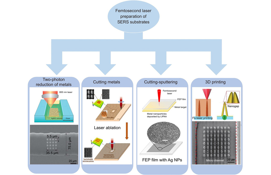
Overview: Surface-Enhanced Raman spectroscopy (SERS) is a highly sensitive and high-resolution molecular recognition technique with important applications in many fields. As an emerging low-cost, high-resolution, and highflexibility micro-nano processing method, femtosecond laser direct writing has been widely used in the field of preparing SERS substrates. Compared with traditional processing methods for preparing SERS substrates, femtosecond laser direct writing processing has certain advantages in terms of flexibility, three-dimensional molding, processing material range, processing accuracy, and other aspects. In this review, we classify the processing methods of femtosecond laser preparation of SERS substrates into four categories, including femtosecond laser two-photon metal reduction, femtosecond laser cutting metal, femtosecond laser cutting-sputtering, and femtosecond laser 3D printing. Femtosecond laser two-photon metal reduction uses the two-photon reduction effect to reduce metal cations in metal solutions to metals, such as silver ions in silver nitrate solutions to silver nanoparticles. This method is suitable for the one-step preparation of SERS substrates in closed microchannels. Femtosecond laser cutting metal directly prepares the SERS substrate structure on a metal substrate. This method takes advantage of the high peak power of the femtosecond laser to ablate the surface of the metal sample to obtain a patterned surface structure. At the same time, femtosecond laser ablation produces particle fragments, which are usually redeposited on the patterned surface, resulting in SERS "hot spots". Femtosecond laser direct cutting of metal can prepare SERS substrates in one step, which has the advantages of high processing efficiency and simple processing and is more conducive to the application of large-scale production of practical SERS detection. Femtosecond laser cutting-sputtering is to process any structure on non-metallic substrates such as polymers and then sputtering/evaporating metal nanoparticles on the surface of the structure. This method can prepare transparent and flexible SERS substrates, which are rich in application scenarios. Femtosecond laser 3D printing is to use the three-dimensional processing ability of femtosecond lasers to obtain rich "hot spots" by designing the structure of SERS substrates, and then using template-guided self-assembly technology with different driving forces to deposit/evaporate metal nanoparticles at designated locations. In this paper, we first introduce the current methods for preparing SERS and then conduct a comprehensive review of the processing methods of four femtosecond lasers to prepare SERS substrates. Finally, the advantages and disadvantages of the four femtosecond laser preparation methods for SERS substrate are briefly summarized, and the development prospects of this technology are prospected, aiming to provide it for future related research.
表面增强拉曼光谱 飞秒激光直写 微纳加工 SERS基底 SERS femtosecond laser direct writing micro/nano processing SERS substrate 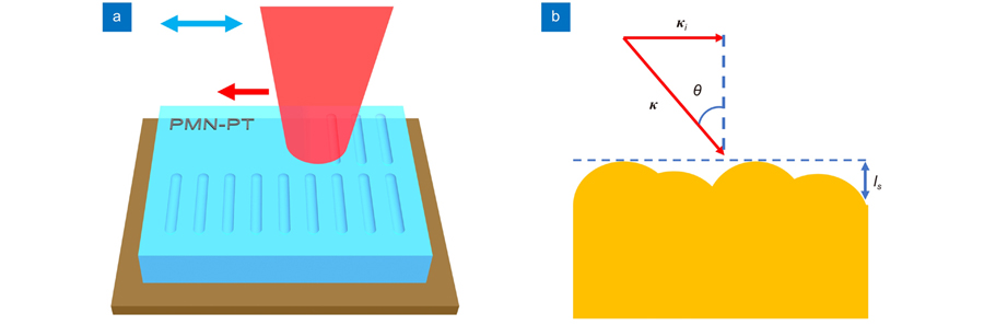
1 南开大学电子信息与光学工程学院微尺度光学信息技术科学重点实验室,天津 300350
2 山东大学晶体材料国家重点实验室,山东 济南 250100
Overview: With the development of modern manufacturing, the size of optical devices is gradually developing towards miniaturization, and integrated optics is also developing to become a topical area of research for many scholars. One of the methods used for producing micro/nano optical devices is femtosecond laser direct writing, a fine three-dimensional processing technique that has been extensively studied by many scholars for its applicability to most materials and can be applied to the fabrication of a wide range of optical devices. Micro/nano-optical devices prepared by femtosecond laser direct writing in crystals have been applied in a broad range of applications in different wavelengths. PMN-PT crystal with relaxed ferroelectric has attracted much attention in recent years for its superior piezoelectric property and large electromechanical coupling coefficient, and its application in the infrared band is more prominent, so the fabrication of the optical devices based on PMN-PT crystal has gradually become a relevant research hotspot. The LIPSS is one of the micro/nano-structures that can be processed by femtosecond laser direct writing. The LIPSS is prevalent in many materials and has been found in metals, semiconductors, dielectrics, etc. Similarly, LIPSS can be induced by femtosecond lasers in PMN-PT crystal. The LIPSS has a wide range of applications in the fields of anti-reflectivity, permanent coloration, and wettability. Nevertheless, the physical processes and the mechanisms involved in the formation of LIPSS have different interpretations in different materials. In this paper, we describe the LIPSS induced by femtosecond laser on the surface of the PMN-PT crystal and characterize it theoretically. We have achieved a change in the period of the LIPSS from 750 nm to 3000 nm after experimenting with different laser parameters. Afterward, we simultaneously obtained the phase transition of the LIPSS in PMN-PT crystal through temperature modulation, and this phase transition can be analyzed by the variation of the Raman spectra. At the same time, we have obtained the Curie temperature for the LIPSS structure that is approximately 10 ℃ lower than that of the PMN-PT crystal and have analyzed the phase transition process through the structural properties of the PMN-PT crystal. The results of our experiments and analyzes on the LIPSS in PMN-PT crystal reported in this paper can provide some experience for the subsequent development of the optical devices related to the LIPSS in PMN-PT crystal.
飞秒激光直写 表面周期结构 PMN-PT晶体 相变 femtosecond laser direct writing LIPSS PMN-PT crystal phase transition 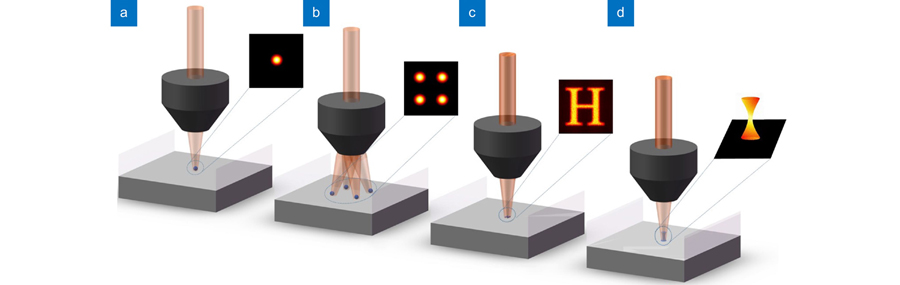
1 之江实验室智能芯片与器件研究中心,浙江 杭州 311121
2 浙江大学光电科学与工程学院极端光学技术与仪器全国重点实验室,浙江 杭州 310027
3 上海电力大学电子与信息工程学院,上海 200090
4 浙江大学杭州国际科创中心, 浙江 杭州 311200
Overview: Two-photon lithography (TPL) has been a research hotspot in 3D micro/nano writing technology due to its characteristics of high resolution, low thermal influence, a wide range of processed materials, low environmental requirements, and 3D processing capability. It has shown unique advantages in the fields of life science, material engineering, micro/nano optics, microfluidic, micro machinery, and so on. This paper summarizes the research works done by researchers on different writing methods to improve TPL processing efficiency. Single-beam writing is the main method for TPL, which mainly depends on the speed of the scanning device. Single-beam writing has the advantages of simple system and high-quality beam, and it is easy to combine various effects to improve writing results. It mainly includes scanning modes based on the translation stage, galvo, polygon laser scanner, and acousto-optic deflector (AOD) (Fig. 2). All these modes have advantages and disadvantages. As for the scanning speed comparison, polygon laser scanner and AOD have relatively faster writing rates (faster than m/s). Multi-foci parallel lithography can obviously promote efficiency, elevating the speed by dozens or even hundreds of thousands of times, mainly based on spatial light modulator (SLM), digital micromirror device (DMD), microlens array (MLA), diffractive optical elements (DOE), multi-beam interference, and so on (Figs. 3-15). Multi-foci parallel lithography based on SLM is most widely used owing to its high efficiency and ability to flexible and independent control of each single beam, but the refresh rate is still insufficient. DMD has a higher refreshing rate (32 kHz), but the state-of-the-art beam parallelism realized by DMD is severely limited. More parallel beams are further required for improving the processing efficiency. The 2D pattern exposure method based on SLM or DMD can further improve the TPL efficiency with the superiority of generating flexibly designed pattern (Figs. 16-18). However, the 2D projection exposure technology is still difficult to achieve high writing precision, especially the axial resolution. An available method to improve the axial precision is spatially and temporally focusing an ultrafast laser to implement a strong intensity gradient at the spatial focal plane that restricts polymerization within a thin layer. The 3D projection method will be the most efficient writing method in the future, especially in 3D device processing (Figs. 19-20). Researchers used this technique to make hollow tubular and conical helices structures, increasing the processing speed by 600 times. However, the research results show that the current 3D projection can only process simple 3D structures. Further researches on 3D exposure processing of complex structures are expected, which will effectively expand its application in various fields. Authors believe that with the effort of researchers on efficiency improvement gradually, TPL can further highlight its advantages to promote the development of life science, materials engineering, micro-nano optics, and many other fields.
飞秒激光直写 双光子光刻 单光束扫描 多焦点并行 面曝光 体曝光 femtosecond laser direct writing two-photon lithography single-beam scanning multi-focus parallelism pattern projection 3D projection exposure 


