High-speed GeSn resonance cavity enhanced photodetectors for a 50 Gbps Si-based 2 μm band communication system
1. INTRODUCTION
The capacity of fiber optic communication networks is growing significantly owing to the rapid development of information technologies such as cloud computing, industrial internet, and 5G wireless communication technology. However, the capacity of single core optical fibers has reached the Shannon transmission limit due to the nonlinear effects of optical fibers and amplifier bandwidth [1]. The further expansion of the transmission capacity of optical fibers is a crucial issue in optical fiber communication technology. Several methods have been proposed in previous studies to improve the capacity of communication systems by manipulating photons in a multidimensional approach. These include wavelength division multiplexing (WDM), time division multiplexing, mode division multiplexing, and polarization multiplexing [2,3].
Among the various existing transmission technologies, increasing the spectral bandwidth is expected to efficiently overcome the capacity bottleneck of single core optical fibers and is an important technique for future broadband optical communication networks. Furthermore, it ensures compatibility with conventional multiplexing and high-order modulation technologies, which can solve the capacity crisis encountered by single core optical fiber. Recently, with the development of the thulium doped fiber amplifier (TDFA) and low-loss hollow core photonic bandgap fiber (HC-PBGF), the spectral bandwidth of the 2 μm band reached 200 nm, which is approximately six times higher than that of the traditional C band [4]. Therefore, the spectral bandwidth technology presents considerable potential for expanding the optical communication capacity.
The Si-based CMOS process is the most widely used technology in the semiconductor industry, which can realize large-scale integrated manufacturing and reduce the cost of the chips. Si photonics has been applied widely in O and C band telecommunication owing to the CMOS technology. Therefore, a Si-based 2 μm optical communication system can significantly help in solving the fiber “capacity crisis.” Extensive research has been conducted on high-speed Si-based photonic devices operated at the 2 μm over the last decade. Examples of such devices include Si-based 2 μm Mach–Zehnder modulators [5], thermo-optically tunable waveguide array gratings with modulation speeds up to 80 Gbps [6], and Si photonic array waveguide gratings with 64 channels [7]. Significant progress has also been made in the development of group IV detectors that are compatible with CMOS technology as they are key components in optical communication networks. As a group IV semiconductor, the GeSn alloy exhibits an adjustable bandgap by changing the Sn content in the alloy, which is the ideal material for fabricating 2 μm band photodetectors.
GeSn photodetectors with 3-dB bandwidth up to 30 GHz at 2 μm have been reported in previous studies. However, their responsivity is only 0.014 A/W due to the low Sn content of the active GeSn layer [8]. Increasing the absorption efficiency, either by enhancing the optical absorption path length or the material absorption efficiency, is the most effective method to achieve the high responsivity. The semiconductor absorption efficiency at a given wavelength increases exponentially with the decreasing bandgap. Therefore, growing a high Sn content GeSn layer can effectively improve the absorption at the 2 μm band. Moreover, the resonance cavity-enhanced photodetector (RCE-PD) structure is widely applied to enhance the interaction between the photons and absorption layers, which can also help in increasing the light utilization [9–12].
In this study, we have designed and fabricated the GeSn RCE-PD with a high Sn content GeSn active layer by combining light field regulation and Sn component engineering. When compared to devices without designing reflectors, the responsivity at the wavelength 2 μm of the device has increased by approximately 2.5 times, reaching 0.49 A/W. This external quantum efficiency (EQE) is approximately 30 times higher than that reported by the high-speed GeSn detector reported in previous literature [8]. The GeSn RCE-PD exhibits a cutoff wavelength of approximately 2750 nm and presents strong responsivity encompassing the entire 2 μm band. The 3-dB bandwidth of the device under reaches 40 GHz at 2 μm. Consequently, a 2 μm band communication system is demonstrated, and a clear eye diagram is obtained at 50 Gb/s by using GeSn RCE-PD. This demonstrates the considerable potential presented by Si photonics for next generation optical communication, along with the significant expansion of the fiber capacity.
2. DEVICE DESIGN AND MATERIAL GROWTH
The Ge detector cannot be operated efficiently beyond the optical communication L band due to the direct bandgap of Ge of approximately 1550 nm. By alloying the Ge with Sn, the GeSn alloys have achieved a narrower bandgap than Ge, which can extend the detector’s operation range up to the 2 μm band. The absorption coefficient is closely correlated to the bandgap. Although higher Sn content GeSn can provide a greater absorption coefficient, it is difficult to grow a thick high Sn content GeSn layer on the Ge buffer due to the large lattice mismatch between the GeSn and Ge. Tran
Figure 1(a) presents a schematic diagram of the GeSn RCE structure designed in this study. An Au mirror is deposited under the buried silicon oxide of SOI as a bottomed reflector, and a double layer anti-reflective layer comprising and is used for the top reflector. The thickness of the GeSn absorption layer and the Ge buffer layer is optimized to enhance the light absorption in the GeSn layer at the 2 μm band. The refractive index of GeSn is calculated through experimental fitting parameters [14]. Figure 1(b) presents the FDTD simulation results of the normalized electric field intensity inside the photodetectors with and without reflectors. The optical field pattern demonstrates that light oscillates between the -type GeSn capped layer and the bottom buried oxide (BOX) layers, creating a vertical cavity for the GeSn active layer to enhance the light absorption. The electric field intensity in the GeSn layer is 1.5 times higher than that without reflectors, indicating that light can be effectively enhanced in the designed RCE structure, as shown in Fig. 1(b).
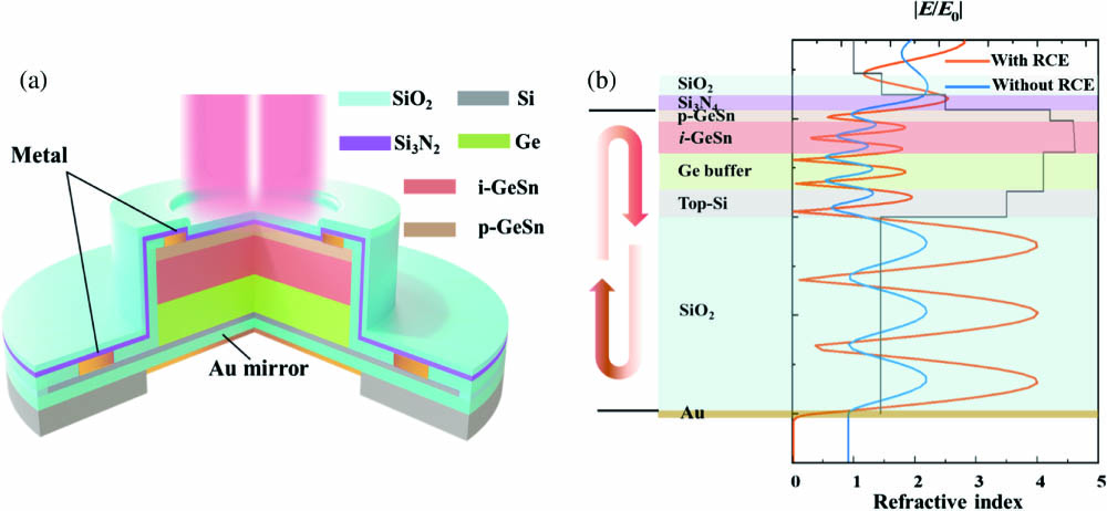
Fig. 1. (a) Schematic diagram of the 2 μm RCE-PD; (b) according to the finite difference-time domain (FDTD) method, the simulation of the normalized electric field intensity
3. MATERIAL CHARACTERIZATION AND FABRICATION OF DEVICES
The GeSn layer was grown on a standard SOI substrate with 220 nm top -type Si layer and 2 μm buried oxide layer (BOX). The n-type Si layer had peak concentration about , by implanting ions with implantation energy 80 keV and dose . Before the materials were grown, the SOI substrates were cleaned using the radio corporation of America (RCA) wet-chemical cleaning recipe and baked at 300°C in the heat station for degassing. The sample is transported to the growth chamber, and the substrate is then deoxidized at a high temperature for Ge layer growth. A two-step method was used to grow a fully relaxed Ge layer on a Si substrate [8]. First, 70 nm thick Ge was grown at 300°C, which can accommodate most dislocations in this layer and release the strain caused by the large lattice mismatch between Si and Ge. At low temperature, the island growth mode can be avoided and form a flat surface for the latter high temperature Ge layer growth. Then, 330 nm thick Ge layer was grown at 600°C to ensure the high-quality Ge layer for the latter GeSn layer growth. Subsequently, cycle annealing was used to restructure the Ge surface and eliminate dislocations within the Ge buffer layer, forming a high-quality Ge surface. The GeSn layer is then grown with the substrate temperature maintained at 150°C. The GeSn layer was grown by using the Sn component gradient technology, which can control the relaxation process and present a high quality GeSn layer. The Sn content in the GeSn absorption layer increased linearly from 9% to 10.7% within 320 nm. Lastly, a 110 nm thick -type GeSn layer with Sn composition of 3.5% and B concentration of approximately was grown by
Figures 2(a) and 2(b) depict the HR-XRD (004) and (224) curves of the as-grown GeSn film. The figure depicts the peaks of the GeSn graded layer, GeSn capped layer, Ge buffer layer, and SOI substrate. For the GeSn graded layer, one sharp peak and one broad peak are observed in the (004) curves, which is attributed to the fully strained GeSn layer and gradually relaxed GeSn layer. The composition of the as-grown GeSn PD structure can be obtained by using the secondary ion mass spectroscopy (SIMS) test. The GeSn absorption layer with a Sn composition ranging from 9% to 10.8% was successfully grown by applying the Sn compositional gradient method, which is consistent with the design. The lattice constants of the Ge buffer layer and GeSn cap layer are determined using the (004) and (224) planes. The and lattice constants of the Ge buffer layer are 0.564 nm and 0.567 nm, respectively, indicating that the Ge layers are fully relaxed. The and lattice constants of the GeSn cap layer are 0.567 nm and 0.570 nm, which also indicates the fully relaxed state. Based on the Vegard law, the GeSn cap layer has a Sn composition of approximately 2.9% [15]. From the FIB image shown in Fig. 2(d), it can be seen that the RCE structure was fabricated successfully.
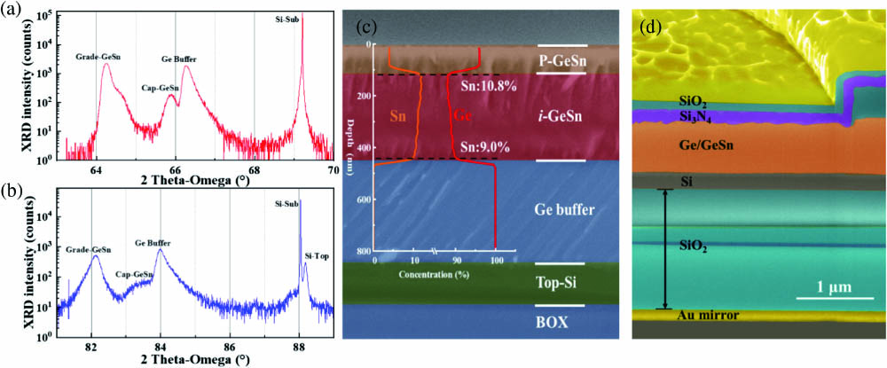
Fig. 2. High resolution
The GeSn, Ge, and Si are etched by using inductively coupled plasma (ICP) etching processes to form a dual mesa structure to reduce the parasitic capacitance of the photodetector. The Ni/Al/Ti/Au metal electrodes were formed following the layer deposition, photolithography, and lift off process. The 217 nm thick layer and 155 nm thick layer were deposited as anti-reflection layers, which were optimized based on FDTD simulation. Subsequently, the thickness of the SOI substrate was reduced to 160 μm, and the silicon was etched onto the BOX layer. An Au layer with a thickness of approximately 100 nm is deposited on the back and serves as the bottom reflector, as shown in Fig. 2(c). For comparison, the GeSn PDs without the RCE structure were also fabricated on the SOI substrate.
4. PHOTOCURRENT AND SPECTRAL RESPONSE
The room temperature responsivity of the GeSn photodetector was measured by using the Agilent B1500A semiconductor parameter analyzer and a 2 μm laser. The incident light was illuminated on the top surface of the photodetector through a single-mode tapered lensed fiber. The photodetector has a good rectification effect, and the contact resistance of the photodetector is , as shown in Fig. 3(a). For GeSn PDs with and without an RCE structure, the responsivity at 2 μm is 0.49 A/W and 0.19 A/W under , respectively, which is enhanced approximately 2.5 times. This concurs with the theory prediction presented above, which states that the light intensity in the GeSn layer is enhanced by approximately 2.25 times when applying the RCE structure. As shown in the inset of Fig. 3(a), it can be seen that the responsivity of the photodetectors remains almost unchanged at the tested optical power range under bias. Among the reported high-speed group IV PIN photodetectors, the GeSn PDs fabricated in this study exhibit the highest responsivity at 2 μm [8,16–18]. This indicates that the GeSn detectors can be operated efficiently on the 2 μm band by using a high Sn content GeSn active layer and an Au mirror as the bottom reflector.
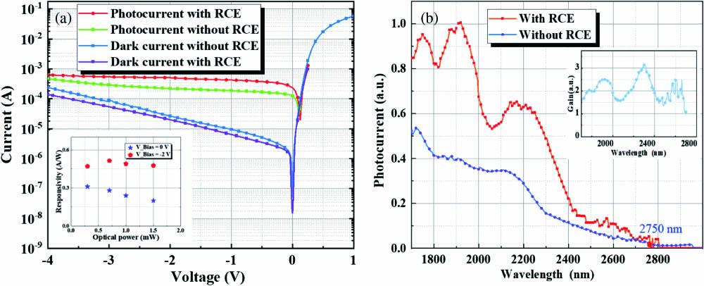
Fig. 3. (a) I-V curves of the GeSn photodetector with a diameter of 20 μm: dark, photocurrent under 2 μm laser incidence with or without RCE structure. The incident light power was 1 mW. The inset shows responsivities of the photodetector with RCE structure under 0 V bias and
To further analyze the RCE structure effect on the GeSn PDs response, the photocurrent spectra of the GeSn PDs with and without the RCE structure were measured by using the Leukos supercontinuum light source and Zolix grating spectrometer. The GeSn PD with RCE structure exhibits strong responsivity from 1700 to 2300 nm, encompassing the entire 2 μm band, as shown in Fig. 3(b). The fabricated GeSn photodetector presents a wide spectral response with a 100% cutoff wavelength of approximately 2750 nm. The highest Sn composition in the Sn gradient GeSn layer is 10.8%, and the relaxation is about 84%, as measured by the XRD and SIMS. According to the deformation theoretical calculation method, the direct bandgap of the top GeSn layer is approximately 0.457 eV, and the indirect bandgap is approximately 0.514 eV. Consequently, the 100% cutoff wavelength is consistent with the theoretical calculation results.
The photodetector with an Au mirror as the bottom reflector exhibits four obvious peaks at 1750 nm, 1920 nm, 2180 nm, and 2600 nm, respectively [12,19]. According to the theory proposed by Ünlü and Strite [20], the resonant peaks in the RCE structure closely correlate with the cavity length. Therefore, the resonant peak can be obtained for specific applications by designing the GeSn layer, Ge buffer layer, and Si layer thickness. The inset of Fig. 3(b) shows that the RCE structure can significantly enhance the responsivity. The RCE structure helps in enhancing the responsivity by approximately 1.5 to 3 times from 1700 to 2400 nm.
5. FREQUENCY RESPONSES
The frequency response of the GeSn RCE PDs was measured by using the vector network analyzer. The 2 μm laser passes through the polarization controller and enters the modulator, where it is modulated by the high-frequency electrical signals generated by the vector network analyzer. The modulated optical signal enters the photodetector through the fiber, where it is converted into an electrical signal by the photodetector. The electrical signal is then connected to the vector network analyzer, where the correlation between the signal strength and frequency is characterized. The detailed measurement information is presented in Ref. [21]. Figure 4(a) depicts the frequency response of the GeSn RCE PDs with different mesa sizes at a 2 μm laser wavelength under . For diameters of 8, 10, 12, 15, and 18 μm, the 3-dB bandwidth () is 40, 24, 20, 16, and 11 GHz, respectively. The of the device with a diameter of 8 μm is higher than 40 GHz, due to the limited modulation speed of the modulator. Figure 4(b) depicts the frequency response of an 8 μm diameter photodiode at different bias voltages. The 3-dB bandwidth increases slightly with the increasing bias and is saturated at . The curves at bias of and are almost overlapped, indicating that the carriers have approached the saturation drift velocity [8].
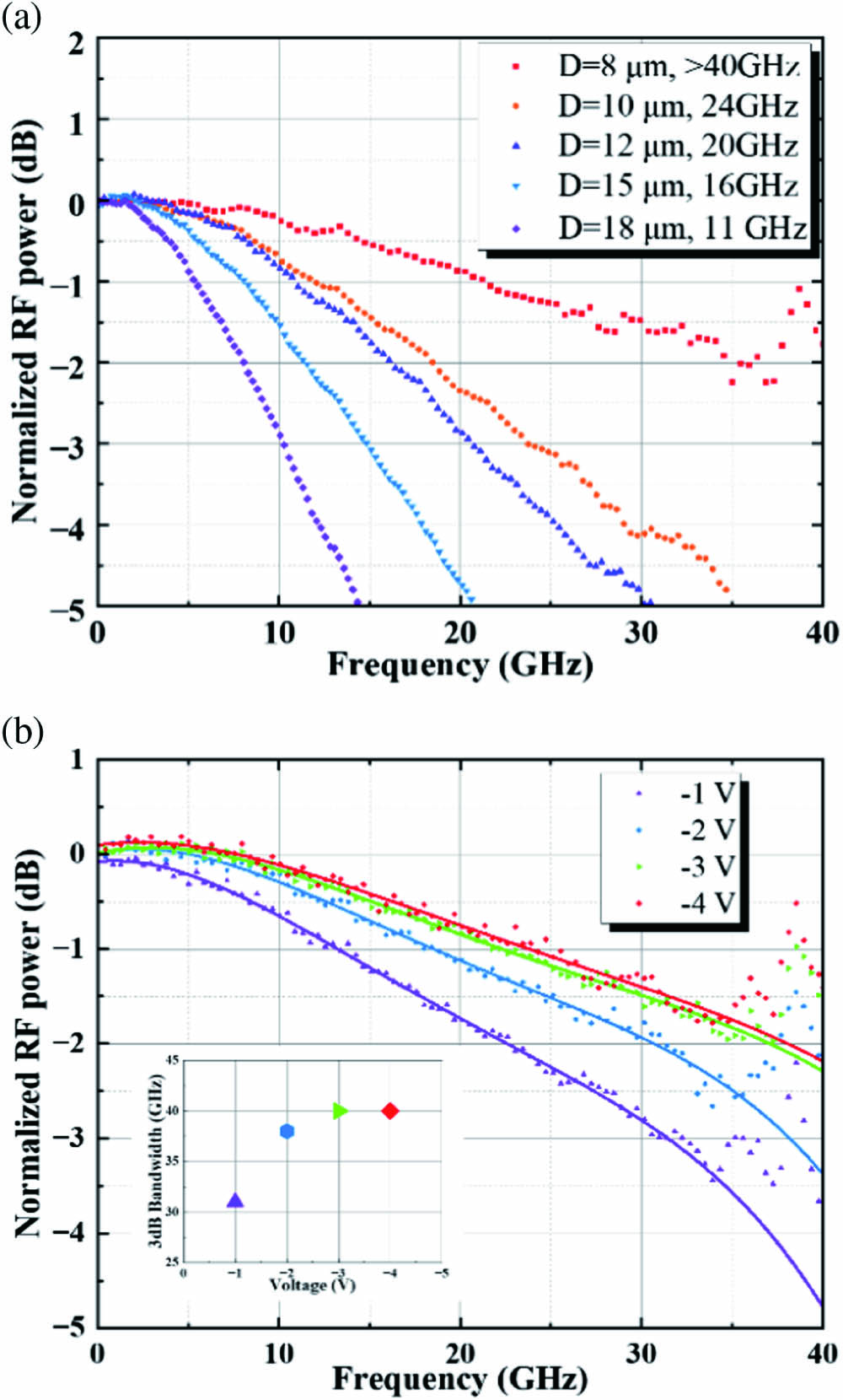
Fig. 4. (a) Normalized frequency responses of PDs with various mesa diameters at 2 μm incident light with
Table 1 summarizes the responsivities and bandwidths of the photodetectors operated at 2 μm. For III-V detectors, it is difficult to achieve high responsivity and high bandwidth at the 2 μm band due to the tradeoff between the carrier transit time and light absorption efficiency [22–26]. For group IV materials, the detection wavelength can be extended to 2 μm by using either Si defect, graphene, or GeSn alloys [21,27–31]. Among these, extensive research has been conducted on the GeSn PDs, whose performance has been enhanced significantly since 2017. In this work, we fabricated GeSn RCE PDs with an active layer grown by using Sn content gradient technology and achieved a responsivity of 0.49 A/W at , which is approximately 30 times higher for GeSn PDs with 30 GHz. The RCE structure can extend the absorption length without increasing the carrier transit time. Compared with the PDs made of III-V materials, GeSn PDs have a relatively high dark current. This can be further reduced by improving the GeSn layer quality and the sidewall passivation technique. Comparison of 3-dB Bandwidth and Responsivity of High-Speed Photodetectors at 2 μm Wavelength in Different Material GroupsReference Structure Material Responsivity (A/W) Jdark at −1 V ( Year [22] PIN InGaAs/GaAsSb 3.7 0.35 2018 [23] WG-PIN InGaAs/GaAsSb 10 0.84 2018 [24] UTC InGaAs/GaAsSb 25 0.07 2019 [25] PIN InGaAs 6 1.34 2008 [26] PIN InGaAs 16 – 25 μA at 2012 [27] APD Si- defects 15 0.3 100 nA at 2015 [28] WG-PIN Graphene 20 0.07 – 2020 [29] PIN GeSn/Ge 1.2 0.23 0.031 2017 [21] PIN GeSn/Ge 10 0.015 0.044 2019 [30] PIN GeSn/Ge 2.7 0.11 0.045 2020 [8] PIN GeSn 30 0.014 0.112 2021 [18] WG-PIN GeSn/Ge 6 0.012 5 μA 2022 [16] PIN GeSn/Ge 1.6 0.232 1.0 2023 [31] PIN GeSn 7.5 at 1550 nm 0.29 9.0 2022 This work RCE-PIN GeSn 0.49 1.4 2023
Figure 5 depicts the benchmark of high-speed 2 μm photodetectors reported in previous literature, which were fabricated either by III-V or IV semiconductors. Although high-speed GeSn detectors have only been reported since 2017, rapid progress has been made since then, and the 3-dB bandwidth of the GeSn PDs in this work presents the highest value of all the reported 2 μm high-speed photodetectors, to the best of our knowledge.
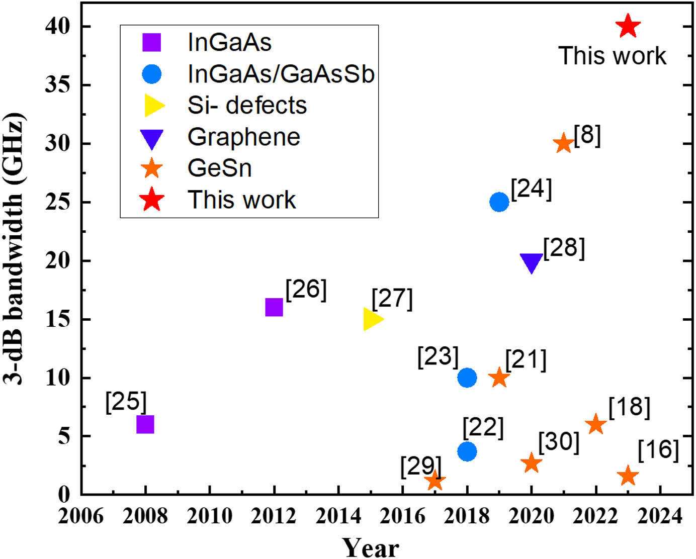
Fig. 5. Comparison of 3-dB bandwidth of high-speed photodetectors at 2 μm band in different groups.
Since the 3-dB bandwidth of the GeSn RCE-PDs can achieve up to 40 GHz, it is necessary to verify the performance of GeSn PDs in silicon-based 2 μm band optical communication. The working mechanism of the silicon-based modulator in the 2 μm band communication system is to use the plasma dispersion effect, which is similar to the Si-based modulator operating in the C band. The of Si modulator at 2 μm wavelength is approximately 7 V, and the designed bandwidth of this modulator is about 30 GHz. The Si depletion modulator and GeSn RCE-PD are connected by fiber to depict the Si-based 2 μm band optical communication system. Figure 6(a) depicts a Si-based communication link for the eye diagram test. The power of the 2 μm laser is amplified by TDFA. After passing through the polarization controller, the 2 μm laser transmitted in the fiber is turned to monochromatic polarized light. The bit pattern generator (12104A) generates high-frequency NRZ signals and loads them onto a Si modulator, which modulates the polarized light. The polarized light carrying the NRZ signal is then coupled into the GeSn RCE detector with a diameter of 8 μm, where the optical signal is converted into an NRZ electrical signal. The optical power coupled into the detector is approximately 0.6 mW. The oscilloscope plots the received electrical signal. Figure 6(b) depicts the eye diagrams of the all Si-based 2 μm band optical communication system. Clear eye diagrams were obtained at transmission rates of 20 Gbps, 30 Gbps, 40 Gbps, and 50 Gbps. Our study presents the implementation of a Si-based 2 μm band optical communication system with 50 Gbps. Additionally, both the modulator and GeSn detector can be prepared using CMOS compatible processes, indicating that the modulator and photodetector can be integrated on a Si chip in future. This indicates that the Si-based 2 μm communication system can be readily applied for huge volume optical communication systems.
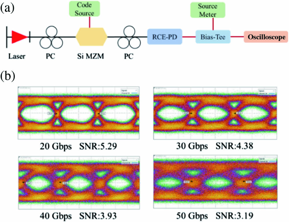
Fig. 6. (a) Demonstration link diagram of 2 μm communication system, consisting of 2 μm laser, polarization controller, Si carrier-depletion Mach–Zehnder modulator, bias-T, etc. Black and red lines represent the optical and electrical connections, respectively. (b) Eye diagrams of 20 Gbps, 30 Gbps, 40 Gbps, 50 Gbps GeSn photodetectors with a diameter of 8 μm at
6. CONCLUSION
In this study, we have successfully designed and fabricated a high-speed GeSn RCE photodetector with high responsivity operating at the 2 μm band by applying a Sn graded component GeSn film as the optical absorption layer. The responsivity reached 0.49 A/W at 2 μm, which is 2.25 times higher than that of devices without an RCE structure. The responsivity at 2 μm achieved in this work is the highest among the reported high-speed group IV photodetectors. The optical path of light in the detector can be effectively extended owing to the resonance enhanced structure, and the GeSn RCE photodetector with RCE structure presents high responsivity between 1700 and 2300 nm. The GeSn RCE photodetector presents the highest 3-dB bandwidth of up to 40 GHz under . A clear eye diagram with a transmission rate of 50 Gbps is demonstrated in a Si-based 2 μm band optical communication system by using GeSn RCE-PD. This study demonstrates the considerable potential presented by Si photonics with GeSn PDs in overcoming the “capacity crisis” faced by optical communication systems by extending the communication wavelength to the 2 μm band.
Article Outline
Jinlai Cui, Jun Zheng, Yupeng Zhu, Xiangquan Liu, Yiyang Wu, Qinxing Huang, Yazhou Yang, Zhipeng Liu, Zhi Liu, Yuhua Zuo, Buwen Cheng. High-speed GeSn resonance cavity enhanced photodetectors for a 50 Gbps Si-based 2 μm band communication system[J]. Photonics Research, 2024, 12(4): 767.
