不同能量质子辐照诱发CCD图像传感器性能退化实验与分析
As a photoelectric image sensor widely used in the field of aeronautics and astronautics, charge-coupled device (CCD) has attracted much attention due to its proton irradiation damage in the space environment. Performance degradation and function failure will be caused by irradiation damage when CCDs are applied to the orbiting satellite or the space imaging system. The irradiation damage effect of CCDs generally includes total ionizing dose, displacement effect, and single event effect. The total ionizing dose and displacement effect will cause permanent damage by influencing the semiconductor material in CCDs to induce oxide defects and interface defects. The single event effect will induce high charge density in the sensitive region of CCDs and disturb the output signal. The damage induced by the single event effect will be gradually recovered in the next signal transfer period. As an important factor causing CCD performance degradation in the space irradiation environment, proton irradiation damage is necessary to be studied, which is of significance to improve the reliability of CCD application in the space irradiation environment. We report the proton irradiation experiments of CCDs with different energy and fluence on proton cyclotrons. The degradation of CCD property parameters such as conversion gain, dark signal, and linear saturation output induced by proton irradiation is analyzed. We hope that our experiment and analysis can be helpful for designers to improve the reliability of CCD applications in space irradiation environments such as space exploration and satellite imaging.
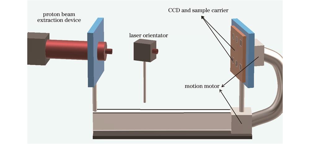
CCD proton irradiation experiments with proton energy of 60 MeV and 100 MeV are carried out on Xi'an 200 MeV Proton Application Facility (XiPAF). The irradiation fluence is 1×10¹⁰, 5×10¹⁰, and 1×1011 cm-2, respectively. All pins of the CCD are offline and unbiased during irradiation. The CCD model used in this experiment is ICX285AL. The pixel size is 6.45 μm×6.45 μm, and the total number of effective pixels is 1392×1024. Its advantages of low noise and high sensitivity meet the requirements of proton irradiation experiments. The CCD parameter test is carried out on the irradiation effect parameter measurement system of photoelectric image sensors based on European standard EMVA1288. The measurement system is composed of a measurement host computer, integrating sphere, sample carrier, and darkroom. The laboratory temperature before and after irradiation is about 25 °C. In this study, the gray value of the dark field image measured in the irradiation effect measurement system of photoelectric image sensors is used as the output signal of the sensor. The value of conversion gain is calculated by the curve of variance gray value and mean gray value, and the dark field image is used to analyze the change in dark signal spike before and after irradiation.
In this study, experiments of proton irradiation of 60 MeV and 100 MeV on CCDs are carried out to analyze the experimental law of CCD performance degradation induced by proton irradiation. The CCD linear part slope of the photon transfer curve produces a certain extent of reduction because the output amplifier of CCDs can be damaged by proton irradiation, which indicates that the conversion gain of CCDs decreases along with the increase in the irradiation fluence (Fig. 3 and Fig. 4). The linear saturation output of CCDs also degrades after proton irradiation with different energy because proton irradiation produces a high concentration of oxide defects and interfacial trapped charge in the CCDs (Fig. 6). In addition, with the increase in irradiation fluence, both conversion gain and linear saturation output degrade to some extent, and proton irradiation with higher energy will induce more serious degradation of conversion gain and linear saturation output than that with lower energy (Fig. 5 and Fig. 6). The study of dark signal shows that the quantity of dark signal spike increases significantly after proton irradiation, and the density of dark signal spike increases with higher energy under irradiation (Fig. 7 and Fig. 8). The dark current of CCDs under proton irradiation raises with the increase in the irradiation fluence, which indicates that both the bulk dark current and surface dark current generated by proton irradiation cannot be ignored (Fig. 9). Furthermore, higher irradiation energy is accompanied by greater increase in dark current. The CCDs irradiated with protons produce ionizing energy loss (IEL) and non-ionizing energy loss (NIEL). The IEL and NIEL are used to evaluate proton irradiation damage of CCDs. Proton ionization damage and proton displacement damage are related to IEL and NIEL, respectively. Overall, the IEL and NIEL induced by proton irradiation of 60 MeV are greater than those induced by proton irradiation of 100 MeV.
The experiments of high energy proton irradiation of 60 MeV and 100 MeV on XiPAF are introduced in this study, and the experimental law of CCD performance degradation induced by proton irradiation is analyzed. The conversion gain, dark signal, and linear saturation output of CCDs degrade obviously, and the dark current significantly increases after proton irradiation. Under the same irradiation fluence, the degradation of conversion gain and linear saturation output induced by proton irradiation of 60 MeV is more serious than that by proton irradiation of 100 MeV, and more dark signal spikes and larger dark currents are produced. The degradation of the above parameters indicates that CCD performance will be seriously affected by proton irradiation. The results show that CCDs are very sensitive to the damage caused by proton irradiation as an image sensor working in the space environment, and the study provides a reference for the research on the damage mechanism of CCD high energy proton irradiation.
1 引言
电荷耦合器件(CCD)作为一种以光注入或电子注入的方式产生电荷、通过在器件栅极加偏压来存储电荷,并运用耗尽层耦合原理与输出放大器进行电荷的传递与输出的光电图像传感器,具有小尺寸、轻质量、低功耗、高量子效率、高图像分辨率和宽动态范围的优点,被广泛应用于航天探测、空间扫描以及卫星观测等领域[1]。然而,由于空间环境具有特殊性,当CCD应用于在轨卫星或航天成像系统时,CCD会产生由辐照损伤引起的性能退化甚至是功能失效现象。CCD的辐照损伤效应一般包括总剂量效应、位移效应和单粒子瞬态效应[2-5]。
总剂量效应和位移效应会通过影响CCD中的半导体材料诱发氧化物缺陷或界面缺陷产生,造成永久性损伤;单粒子瞬态效应会在CCD灵敏区域产生高电荷密度而扰动输出信号,但其造成的损伤会随时间推移逐渐恢复[6]。质子辐照损伤是空间辐射环境中引起CCD性能退化的重要因素,因此研究质子辐照损伤对提高CCD在空间辐射环境中应用的可靠性具有重要意义。
国内外均开展了CCD辐照效应的实验研究。Janesick等[5]首先从科学用CCD的辐照实验中发现了辐照效应诱发传感器损伤的现象。Hopkinson等[4,7-10]对质子和60Co γ射线辐照CCD诱发暗电流、电荷转移效率等性能参数退化的机理进行分析。Germanicus等[11]针对商用CCD开展质子辐照实验,分析了暗信号的退化规律,并提出一种基于马歇尔法预测暗信号退化规律的方法。王祖军等[6,12-13]开展了TCD线阵CCD质子和60Co γ辐照实验,研究了辐照后电荷转移效率以及暗信号等辐照敏感参数的退化机理;近年来,该团队开展了CCD的中子以及中高能量质子辐照实验,研究了中子和不同能量质子辐照面阵CCD诱发损伤的实验规律和机理[14-16]。于庆奎等[17]开展了不同注量下质子和γ射线辐照CCD的实验,研究了评估CCD位移损伤的地面模拟实验方法。文林等[18]开展了面阵CCD辐照实验,分析了质子和γ射线辐照下诱发CCD光响应退化的机制。
虽然国内国外都开展了大量质子辐照实验来研究CCD的辐照损伤效应,但关于质子辐照CCD后引发的转换增益和线性饱和输出退化现象的研究报道相对较少。为了提高CCD在辐射环境中的工作性能,本文介绍了在西安200 MeV质子应用装置(XiPAF)上开展的CCD质子辐照实验,并对辐照损伤引起的转换增益和线性饱和输出退化现象进行分析。通过开展CCD在2个不同能量、3个不同注量下的质子辐照实验,比较辐照前后转换增益、线性饱和输出以及暗信号的变化,深入研究质子辐照引起CCD各项性能参数退化的实验规律和损伤机理。
2 辐照实验
在XiPAF上分别开展了质子能量为60 MeV和100 MeV的CCD质子辐照实验,质子辐照注量分别为1×1010 cm-2、5×1010 cm-2和1×1011 cm-2,
CCD的参数测试在基于欧洲标准EMVA1288搭建的光电图像传感器辐照效应参数测试系统上进行,测试系统由测试上位机、积分球、样品载台、暗室等组成,开展辐照前后的测试时实验室温度在25 ℃左右。
3 实验结果与分析
3.1 转换增益
对每个光电子产生的信号进行测定,可得到传感器的转换增益,它是高灵敏度光电传感器的重要表征参数之一。转换增益表示传感器将光信号转换为电信号的转换系数[20],其定义为
式中:
式中:
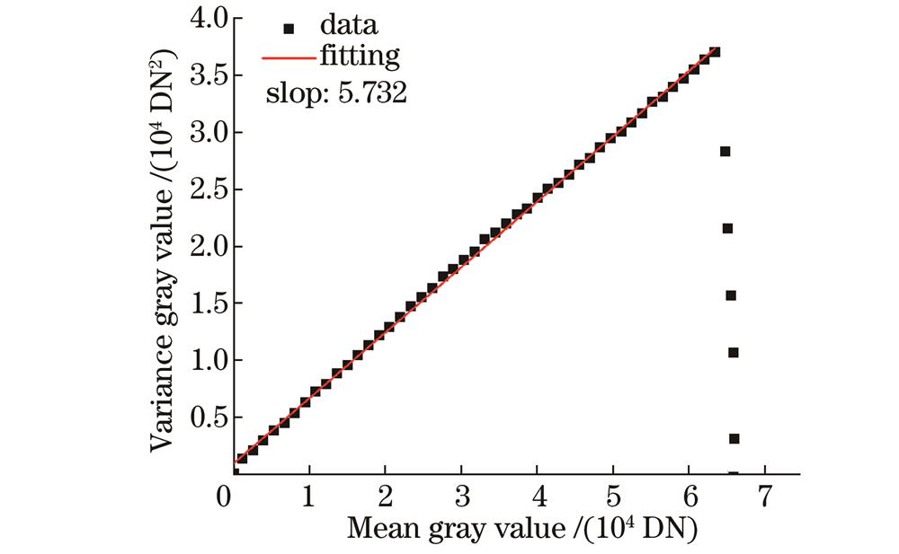
图 2. 质子辐照前CCD方差灰度值与均值灰度值的关系
Fig. 2. Relationship between variance gray value and mean gray value before proton irradiation
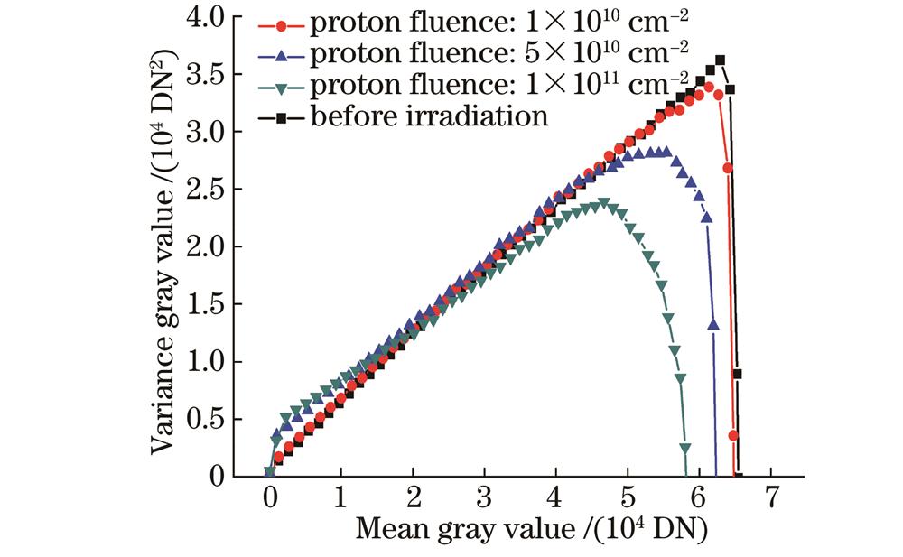
图 3. 60 MeV质子辐照前后CCD方差灰度值与均值灰度值的关系
Fig. 3. Relationship between variance gray value and mean gray value before and after 60 MeV proton irradiation
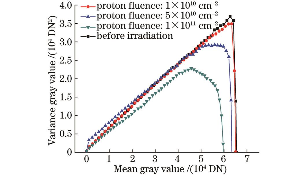
图 4. 100 MeV质子辐照前后CCD方差灰度值与均值灰度值的关系
Fig. 4. Relationship between variance gray value and mean gray value before and after 100 MeV proton irradiation
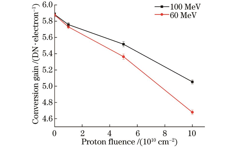
图 5. 转换增益与质子辐照能量和注量的关系
Fig. 5. Relationship between conversion gain with proton irradiation energy and proton fluence
3.2 线性饱和输出
CCD的输出放大器作为信号处理和传输的关键部位,通常用饱和输出来衡量放大器的性能。饱和输出是方差灰度值与辐照程度之间的测量关系的最大值[25]。线性饱和输出表示方差灰度值随辐照变化的线性范围内的最大信号输出。
式中:
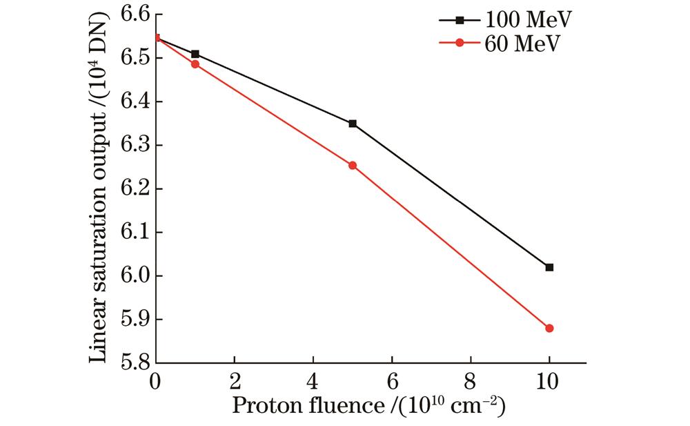
图 6. 线性饱和输出与质子辐照注量的关系
Fig. 6. Relationship between linear saturation output with proton irradiation fluence
3.3 暗信号尖峰
在外界既不施加光照又无偏置电压的情况下,CCD输出的信号称为暗信号。CCD正常工作时MOS电容处于不饱和状态,由半导体材料本身原子振动导致的电子跃迁使得MOS电容随时间的推移趋于饱和,因此在外界既不施加光照又无偏置电压的情况下也会产生少量暗信号[27]。
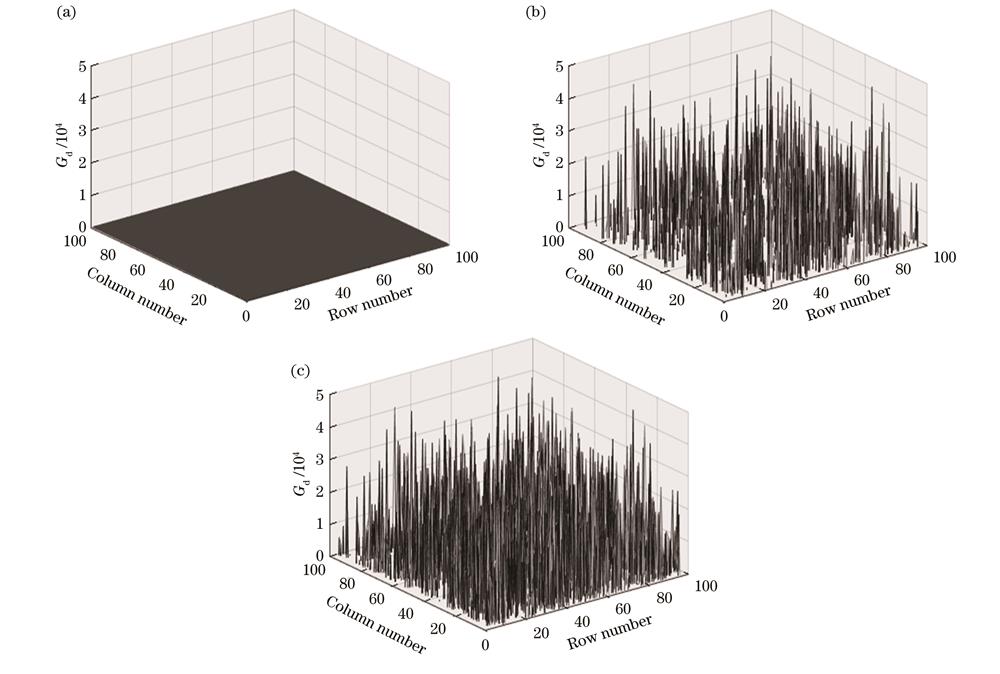
图 7. 60 MeV质子辐照后,不同注量下CCD像元阵列中暗信号尖峰的变化情况。(a)辐照前;(b)质子注量为1×1010 cm-2;(c)质子注量为1×1011 cm-2
Fig. 7. Changes of dark signal spike in CCD pixel array after 60 MeV proton irradiation under different fluence. (a) Before irradiation; (b) proton fluence is 1×1010 cm-2; (c) proton fluence is 1×1011 cm-2
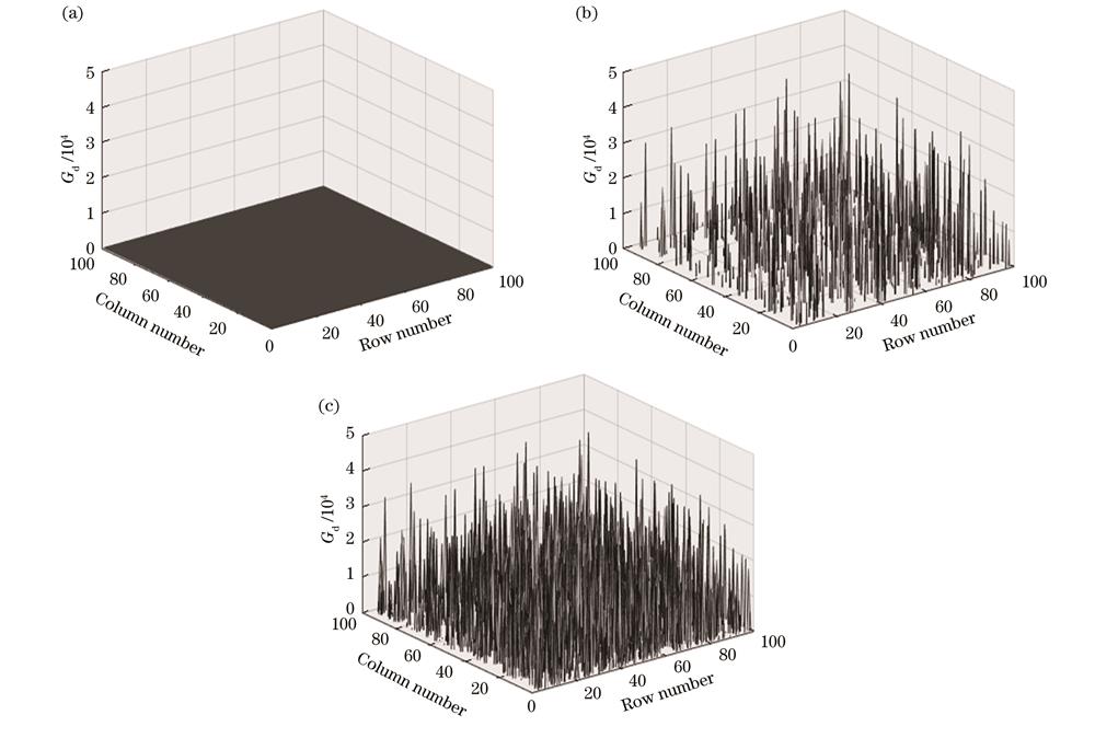
图 8. 100 MeV质子辐照后,不同注量下CCD像元阵列中暗信号尖峰的变化情况。(a)辐照前;(b)质子注量为1×1010 cm-2;(c)质子注量为1×1011 cm-2
Fig. 8. Changes of dark signal spike in CCD pixel array after 100 MeV proton irradiation under different fluence. (a) Before irradition; (b) proton fluence is 1×1010 cm-2; (c) proton fluence is 1×1011 cm-2
3.4 暗电流
暗电流是指在没有光照射的状态下,在光电器件内部流动的电流[29]。
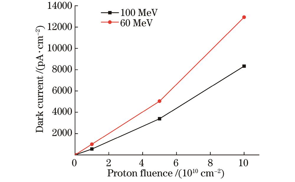
图 9. 暗电流与质子辐照能量和注量的关系
Fig. 9. Relationship between dark current with proton irradiation energy and fluence
质子电离损伤会诱发CCD栅极氧化层缺陷以及Si和SiO2的界面态使得电子产生跃迁,进而导致表面暗电流增大,根据Hopkinson[9]的理论,表面暗电流的计算公式可写为
式中:
质子位移损伤会使CCD产生体缺陷,进而导致体暗电流增加。令
式中:
则体暗电流的计算公式为
式中:
从
4 总结
介绍了在XiPAF上开展的60 MeV和100 MeV高能质子辐照实验,研究了质子辐照诱发CCD性能退化的实验规律。在质子辐照后,CCD的转换增益、暗信号以及线性饱和输出产生明显退化,且暗电流在质子辐照后明显增大。在相同注量下,60 MeV质子辐照诱发的转换增益和线性饱和输出退化比在100 MeV质子辐照下更严重,产生更多的暗信号尖峰以及更大的暗电流,上述参数的退化表明CCD性能会受到质子辐照的严重影响。本次实验结果表明,CCD作为工作在空间辐射环境中的图像传感器件,对质子辐照产生的损伤非常敏感。因此,本研究结果为开展CCD高能质子辐照损伤机理研究提供实验数据参考。
下一步将在XiPAF上继续深入开展不同能量质子对不同类型CCD的辐照实验,以进一步研究CCD质子辐照后的转换增益及线性饱和输出等辐射敏感参数的退化规律和损伤机理。
[1] 张坤. 国外星用CCD图像传感器的研制现状[J]. 中国电子科学研究院学报, 2007, 2(3): 324-328.
Zhang K. Abroad development status of CCD image sensors usedin secondary planet[J]. Journal of China Academy of Electronics and Information Technology, 2007, 2(3): 324-328.
[2] 王祖军, 黄绍艳, 刘敏波, 等. CCD位移辐射效应损伤机理分析[J]. 半导体光电, 2010, 31(2): 175-179.
Wang Z J, Huang S Y, Liu M B, et al. Analysis of the displacement damage mechanism of radiation effects in CCD[J]. Semiconductor Optoelectronics, 2010, 31(2): 175-179.
[3] 王祖军, 唐本奇, 肖志刚, 等. CCD电离辐射效应损伤机理分析[J]. 核电子学与探测技术, 2009, 29(3): 565-570, 619.
Wang Z J, Tang B Q, Xiao Z G, et al. The analysis of mechanism on ionization radiation damage effects on CCD[J]. Nuclear Electronics & Detection Technology, 2009, 29(3): 565-570, 619.
[4] Hopkinson G R, Dale C J, Marshall P W. Proton effects in charge-coupled devices[J]. IEEE Transactions on Nuclear Science, 1996, 43(2): 614-627.
[5] Janesick J, Elliott T, Pool F. Radiation damage in scientific charge-coupled devices[J]. IEEE Transactions on Nuclear Science, 1989, 36(1): 572-578.
[6] 王祖军. 电荷耦合器件质子辐照损伤实验及数值模拟研究[D]. 北京: 清华大学, 2011.
WangZ J. Research on proton radiation effects on charge coupled device with experiment and simulation methods[D]. Beijing: Tsinghua University, 2011.
[7] Hopkinson G R, Mohammadzadeh A. Comparison of CCD damage due to 10- and 60-MeV protons[J]. IEEE Transactions on Nuclear Science, 2003, 50(6): 1960-1967.
[8] Hopkinson G R. Proton-induced changes in CTE for n-channel CCDs and the effect on star tracker performance[J]. IEEE Transactions on Nuclear Science, 2000, 47(6): 2460-2465.
[9] HopkinsonG R. Radiation-induced dark current increases in CCDs[C]//RADECS 93. Second European Conference on Radiation and its Effects on Components and Systems, September 13-16, 1993, Saint Malo, France. New York: IEEE Press, 2002: 401-408.
[10] Hopkinson G R. Cobalt60 and proton radiation effects on large format, 2-D, CCD arrays for an Earth imaging application[J]. IEEE Transactions on Nuclear Science, 1992, 39(6): 2018-2025.
[11] Germanicus R, Barde S, Dusseau L, et al. Evaluation and prediction of the degradation of a COTS CCD induced by displacement damage[J]. IEEE Transactions on Nuclear Science, 2002, 49(6): 2830-2835.
[12] 王祖军, 唐本奇, 肖志刚, 等. 质子辐照电荷耦合器件诱导电荷转移效率退化的实验分析[J]. 物理学报, 2010, 59(6): 4136-4142.
Wang Z J, Tang B Q, Xiao Z G, et al. Experimental analysis of charge transfer efficiency degradation of charge coupled devices induced by proton irradiation[J]. Acta Physica Sinica, 2010, 59(6): 4136-4142.
[13] 王祖军, 张勇, 唐本奇, 等. TCD132D线阵CCD总剂量效应的实验分析[J]. 电子器件, 2010, 33(1): 18-21.
Wang Z J, Zhang Y, Tang B Q, et al. Analysis of experiments on total dose radiation effects on TCD132D linear CCD[J]. Chinese Journal of Electron Devices, 2010, 33(1): 18-21.
[14] 王祖军, 薛院院, 王迪, 等. 西安200 MeV质子应用装置200 MeV质子辐照CCD的实验结果与分析[J]. 现代应用物理, 2021, 12(2): 020604.
Wang Z J, Xue Y Y, Wang D, et al. Charge coupled device irradiated by 200 MeV protons at Xi’an 200 MeV proton application facility[J]. Modern Applied Physics, 2021, 12(2): 020604.
[15] Wang Z J, Xue Y Y, Xu R, et al. Charge transfer inefficiency increase of the CCD detector induced by proton and neutron irradiations[J]. Nuclear Instruments and Methods in Physics Research Section A, 2020, 978: 164431.
[16] Wang Z J, Xue Y Y, Zhang F Q, et al. Radiation damage evaluation of the CCD detector induced by high energy protons[J]. Nuclear Instruments and Methods in Physics Research Section A, 2019, 924: 219-224.
[17] 于庆奎, 唐民, 朱恒静, 等. 用10 MeV质子和钴60 γ射线进行CCD空间辐射效应评估[J]. 航天器环境工程, 2008, 25(4): 391-394, 300.
Yu Q K, Tang M, Zhu H J, et al. Experimental investigation on radiation damage on CCD by 10 MeV proton and cobalt 60 gamma[J]. Spacecraft Environment Engineering, 2008, 25(4): 391-394, 300.
[18] 文林, 李豫东, 郭旗, 等. γ射线及质子辐照导致CCD光谱响应退化的机制[J]. 发光学报, 2018, 39(2): 244-250.
[19] 孙茂多, 董全林, 赵伟霞, 等. 基于CPLD的面阵CCD驱动电路设计[J]. 现代电子技术, 2014, 37(23): 142-145.
Sun M D, Dong Q L, Zhao W X, et al. Design of array CCD driving circuit based on CPLD[J]. Modern Electronics Technique, 2014, 37(23): 142-145.
[20] Beecken B P, Fossum E R. Determination of the conversion gain and the accuracy of its measurement for detector elements and arrays[J]. Applied Optics, 1996, 35(19): 3471-3477.
[21] 冯婕, 李豫东, 文林, 等. CMOS图像传感器光子转移曲线辐照后的退化机理[J]. 光学 精密工程, 2017, 25(10): 2676-2681.
[22] Wang Z J, Xue Y Y, Guo X Q, et al. Measurement and analysis of the conversion gain degradation of the CIS detectors in harsh radiation environments[J]. Nuclear Instruments and Methods in Physics Research Section A, 2018, 895: 35-39.
[24] Jun I, Xapsos M A, Messenger S R, et al. Proton nonionizing energy loss (NIEL) for device applications[J]. IEEE Transactions on Nuclear Science, 2003, 50(6): 1924-1928.
[26] Schwank J R, Shaneyfelt M R, Fleetwood D M, et al. Radiation effects in MOS oxides[J]. IEEE Transactions on Nuclear Science, 2008, 55(4): 1833-1853.
[27] 邹异松, 刘玉凤, 白廷柱. 光电成像原理[M]. 北京: 北京理工大学出版社, 1997: 357.
ZouY S, LiuY F, BaiT Z. Photoelectricity imaging theory[M]. Beijing: Beijing Institute of Technology Press, 1997: 357.
[28] 王祖军, 薛院院, 刘卧龙, 等. CMOS图像传感器西安200 MeV质子应用装置H-辐照效应实验研究[J]. 现代应用物理, 2021, 12(3): 030604.
Wang Z J, Xue Y Y, Liu W L, et al. H- beams irradiation effect of CMOS image sensor at Xi’an 200 MeV proton application facility[J]. Modern Applied Physics, 2021, 12(3): 030604.
[29] 刘伟胜. 太阳能技术用语集[M]. 石家庄: 河北科学技术出版社, 1989: 391.
LiuW S. Energy technology glossary[M]. Shijiazhuang: Hebei Science & Technology Press, 1989: 391.
[30] Hardy T D, Deen M J, Murowinski R. Effects of radiation damage on scientific charge coupled devices[J]. Advances in Imaging and Electron Physics, 1999, 106: 1-96.
黄港, 王祖军, 吕伟, 聂栩, 赖善坤, 晏石兴, 王敏文, 卓鑫, 于俊英, 王忠明. 不同能量质子辐照诱发CCD图像传感器性能退化实验与分析[J]. 光学学报, 2023, 43(11): 1123001. Gang Huang, Zujun Wang, Lü Wei, Xu Nie, Shankun Lai, Shixing Yan, Minwen Wang, Xin Zhuo, Junying Yu, Zhongming Wang. Experiment and Analysis of Performance Degradation of CCD Image Sensors Induced by Proton Radiation with Different Energy[J]. Acta Optica Sinica, 2023, 43(11): 1123001.
