晶圆金属表面纳米颗粒暗场检测系统设计
Defect detection is an essential process for realizing superdiffraction fabrication based on metal film layer excitation surface plasmons. However, the light source of most existing advanced defect detection equipment operates in the deep ultraviolet band (DUV), which is within the light-sensitive range of DUV photoresists such as KrF. The overlap of working wavelengths between the defect detection equipment and the DUV photoresist can result in a loss of photoresist efficacy. Furthermore, to avoid the influence of the detection equipment's working wavelength on the photoresist when DUV equipment is used to detect particles on the surface of the film, it is necessary to tune the equipment's incident intensity several times. Moreover, the equipment parameters after tuning are only effective for a single film structure. It is necessary to retune equipment parameters when changing the thickness, material, and the number of film layers, which is time consuming and labor intensive. Therefore, a defect-detection device with a wide range of applications that avoids photoresist-sensitive bands must be developed to address this challenge.
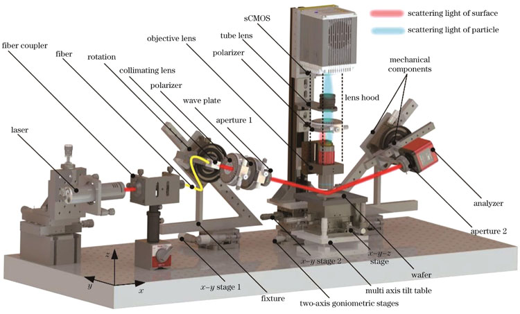
In this study, visible laser polarization defect detection equipment consisting of three parts: polarization modulation, dark-field detection, and motion control (Fig. 8), is theoretically and experimentally demonstrated. A more sensitive scientific CMOS (sCMOS) is used to detect particle scattering signals. The equipment utilizes the polarization conversion principle of a silver film on the top layer of the wafer surface. By modulating the polarization state and incident angle of the incident light, the scattered light polarization states on the slightly rough silver film surface and the particles on the film surface are different. On the receiving side, the light scattered from the surface of the silver film is partially filtered using a polarization detection device, which improves the signal-to-noise ratio of the particle signal to achieve defect detection.
Based on the aforementioned principles, experimental equipment was developed to verify particle detectability [Fig.8(a)]. Standard polystyrene latex (PSL) spheres with diameters of 100 and 50 nm were used as detection targets. Etching marks on the surface of the silicon wafer were used as the detection area, and subsequent processes such as photoresist spin-coating, magnetron sputtering coating, reactive ion beam etching (AFM surface roughness detection), and particle solution atomization were performed on the wafer [Fig.8(b)]. In this experiment, silver films with different surface roughness were processed by controlling the power and etching time of reactive ion beam etching. After dilution and ultrasonic vibration, the particle solution was sprayed onto the surface of the silver film using an atomizer such that standard PSL particles with diameter 100 and 50 nm were uniformly distributed in the surface labeled area. In addition, the samples were maintained under a vacuum insofar as possible during the experiment to decelerate oxidation of the silver film.
The effect of surface roughness on particle detection was subsequently analyzed. Samples with different surface roughness values were observed using identical camera exposure parameters (Fig.10). Experimental results show that as the silver film surface roughness increases, the background noise obtained from the experiment also increases, which can cover up the signal of small-particle defects and cause misclassification. To reduce the effect of surface roughness on particle detection, a polarization device was introduced into the detection equipment and the effect of the incident light polarization state on the signal-to-noise ratio of particles was analyzed. Based on the results, it can be observed that the signal-to-noise ratio of particles differs with different polarization states of the incident light [Fig. 12(a)?(d)]. In the detection experiment involving 100 nm particles, the single exposure time of this equipment was only 150 μs, which is 4‰ of the DSX1000 dark-field microscope based on white light, and the detection efficiency was significantly improved. Finally, it was confirmed using a scanning electron microscope that the proposed experimental system could detect 61 nm PSL particles [Fig.12(l)].
This study conducted targeted research based on defect detection during the plasmon super-diffraction fabrication of metal film layer surfaces. Background noise was suppressed by the polarization modulation technique, and the PSL particles with diameter of 61 nm on the silver film surface were detected with a 473 nm light source for inspection. The equipment operates in the visible wavelength band, which differs from the sensitive wavelength band of the DUV photoresist, thus, effectively avoiding photoresist failure. The proposed method can be theoretically extended to other wavelengths, which can be flexibly selected according to photoresist sensing characteristics, and can improve particle detectability without loss of photoresist efficacy. The proposed solution has a straightforward structure, high practicality, low cost, and good prospects for application in the field of micro-nano fabrication.
1 引言
表面等离子体(SP)是指金属表面自由电子的一种相干集体振荡[1-2],其可在亚波长区域明显增强电磁场强度,并且其等效波长远小于真空波长。与表面等离子体相关的技术,如超透镜[3-7]、反射腔共振镜[8-10]、双曲超材料[11-12]等技术,在超衍射成像及微纳加工等领域极具发展前景。以简单超透镜模型为例,晶圆表面有底层光刻胶和顶层银膜,通过银膜激发表面等离子体激元干涉可以得到超衍射图形[8],如果银膜表面存在较多的颗粒等缺陷,将极大地影响成像效果,因此需要对其进行表面颗粒检测。
无图案晶圆表面缺陷检测的光学技术主要有干涉法[13-15]、衍射法[16-18]及散射法[19-21]三类,其中散射法中的暗场散射技术具有灵敏度和效率高的特点,因此被广泛应用于实际生产中[21]。散射法通过检测缺陷的散射光来判定表面情况,它通过所建立的标准直径聚苯乙烯乳胶(PSL)颗粒散射光强的“相关曲线”将采集的散射光强度转换为缺陷的等效尺寸[22-23]。由于颗粒散射能的大小与波长呈负相关,因此为了检测到更小的颗粒,商用化设备采用的检测光源逐渐发展到了深紫外,例如美国KLA公司研制的Surfscan系列中的Surfscan SP7XP采用深紫外照明结合多通道探测能满足5 nm节点工艺的缺陷检测需求[24]。国内在这方面的起步较晚,目前最先进的是深圳中科飞测科技股份有限公司(以下简称“中科飞测”)生产的SPRUCE-800,但其即使采用266 nm光源也只能检测到直径为32 nm的颗粒,并且在该检测指标下已经无法保证捕获率。
目前,实验室主要采用暗场缺陷检测设备对带有光刻胶和顶层银膜的超透镜模型进行表面颗粒等缺陷的检测,如果选用基于白光的暗场散射显微镜,如奥林巴斯的DSX1000,不仅难以获得表面缺陷分布全貌,而且颗粒检测能力只能达到100 nm,此外曝光时间还比较长,自动化程度低,采集效率也不高;如果选用深紫外波段的检测设备,如中科飞测的SPRUCE-800,虽然可以解决暗场散射显微镜的不足,但一些紫外光刻胶(KrF、i线等)的感光范围恰好覆盖了入射光波段,易导致光刻胶感光而失效,无法参与后续曝光等工艺。暗场缺陷检测设备在使用过程中往往需要反复摸索其工艺参数以避免光刻胶感光,而且这些工艺参数只对一种模型有效,同时此类设备也极其昂贵。总的来说,当前实验室尚没有一种具有针对性和简易性的低成本专用设备能够弥补以上不足。
笔者设计了一种基于可见波段的激光偏振暗场检测实验验证装置,同时采用灵敏度更高的科研级相机(sCMOS)探测颗粒的散射信号。该装置利用晶圆表面顶层银膜的偏振转换特性,通过调控入射光的偏振态与入射角,使微粗糙银膜表面的弱散射光偏振态与膜层表面颗粒的散射光偏振态产生差异,然后利用偏振器件对来自银膜表面的散射光进行部分滤除,从而降低其进入sCMOS的比例,提高了颗粒的信噪比。实验结果表明,相较于基于白光的暗场散射显微镜,在百纳米级颗粒检测时,本装置单次曝光时间仅为150 μs,并且实测出了均方根(RMS)粗糙度为3.4 nm(评估面积均为1 μm×1 μm)的银膜表面上61 nm的PSL颗粒,在探测极限和工作效率方面都取得了更好的效果;相较于深紫外检测设备,本装置不会使底层光刻胶改性失效。
2 基本原理
暗场物镜收集的光场分为两部分,一是作为信号的颗粒散射场,二是作为噪声的膜层散射场,这是由膜层表面不是理想镜面导致的。在颗粒较大时,信号强度远大于噪声,但随着颗粒减小,信号强度逐渐衰减到噪声水平,甚至更小,检测难度增大。下面对两者进行分析。
2.1 银膜表面的散射
采用微扰理论处理入射光在银膜表面的散射分布。在银膜粗糙度较小的情况下,将膜层表面看作是理想平面与一个小扰动的叠加,由于
式中:

图 1. 理论模型及原理说明。(a)银膜表面的散射;(b)双交互模型原理;(c)偏振调控原理
Fig. 1. Theoretical model and principle description. (a) Scattering of silver film surface; (b) double interaction model principle; (c) principle of polarization modulation
2.2 颗粒在银膜表面的散射
颗粒与银膜之间存在复杂的相互作用,因此颗粒在银膜上的散射不同于其在自由空间的散射,需要进行更全面的考虑。本文采用双交互模型[27-28]分析颗粒在银膜上的散射场,原理如
式中:α表示两入射光的相位差,
式中:
式中:
2.3 偏振转换原理
提高信噪比的原理如
相位差变化为
3 仿真结果
本文采用时域有限差分方法(FDTD方法),结合仿真软件FDTD Solutions,建立了纳米颗粒及表面粗糙度均不同的散射模型,对暗场检测微粗糙银膜表面的纳米颗粒散射进行了仿真分析。
3.1 银膜透射率仿真
激发表面等离子体可以得到超衍射图形,但表面颗粒将影响图形质量,为保证得到高质量图形,需要对表面进行颗粒检测,但目前实验室所使用的SPRUCE-800的266 nm检测光源在检测过程中易透射至光刻胶层,导致光刻胶改性失效。以266 nm作为入射仿真波长,银膜厚度的变化范围为20~60 nm,入射角在0°~80°之间,通过软件建立的仿真模型如

图 2. 透射率仿真模型及结果。(a)仿真模型;(b)透射率仿真结果;(c)经266 nm光检测后的K4光刻胶表面
Fig. 2. Transmission simulation model and simulation result. (a) Simulation model; (b) transmittance simulation result; (c) K4 photoresist surface detected by 266 nm light
3.2 颗粒在明暗场检测技术下的仿真
采用可见光(473 nm)作为测试光源,利用构建S矩阵的方法仿真得到了银膜表面半径为100 nm的PSL颗粒在明暗场两种检测方法下的检测结果。入射光通过数值孔径为0.82的显微物镜对表面进行照明,暗场收集的数值孔径范围为0.82~0.92。明场检测仿真结果如
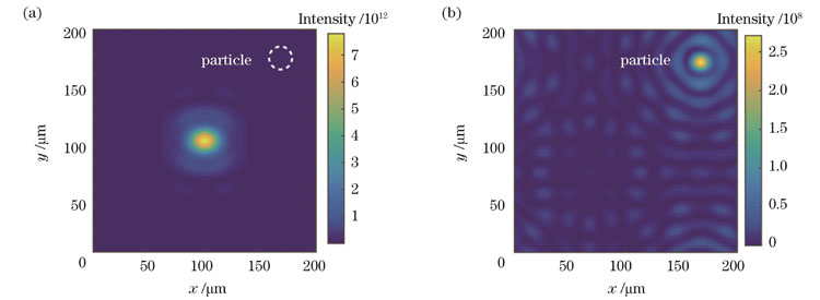
图 3. 明暗场检测仿真图像。(a)明场仿真结果;(b)暗场仿真结果
Fig. 3. Simulation results of brightness and dark fields detection. (a) Brightness field simulation result; (b) dark field simulation result
3.3 颗粒在银膜表面的散射场仿真
利用全场散射源(TFSF)对银膜表面的纳米颗粒进行散射场仿真与远场投影,以473 nm的p、s偏振光入射,同时使用PSL与SiO2两种不同材料的纳米颗粒,颗粒半径扫描以20 nm为梯度,扫描范围为20~80 nm。两种颗粒散射能的仿真结果如
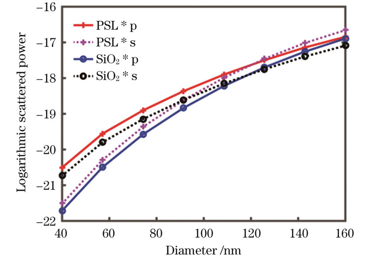
图 4. PSL与SiO2颗粒在p光和s光入射下的散射能
Fig. 4. Scattering energy of PSL and SiO2 particles under p and s light incidence
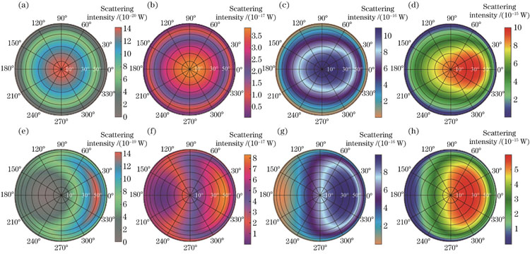
图 5. 不同直径的PSL颗粒在p光和s光入射下的散射场分布。(a)~(d)半径分别为20、40、60、80 nm的PSL颗粒在p光入射下的散射能空间分布;(e)~(h)半径分别为20、40、60、80 nm的PSL颗粒在s光入射下的散射能空间分布
Fig. 5. Scattering field spatial distribution of PSL particles with different diameters under p and s light incidence. (a)‒(d) Spatial distribution of scattering energy of PSL particles with radius of 20,40,60,80 nm under p light incidence; (e)‒(h) spatial distribution of scattering energy of PSL particles with radius of 20, 40, 60,80 nm under s light incidence
3.4 微粗糙银膜表面的散射仿真
采用平面波入射+Bloch边界条件分析了均方根(RMS)粗糙度为8 nm的微粗糙银膜表面的双向散射分布函数(BSDF),观察微粗糙表面散射光的空间分布。入射波段为473 nm,依次改变入射光角度为0°、30°、60°,得到的由表面粗糙度引起的空间散射角度分布如

图 6. 不同入射角下的仿真结果。(a)0°入射角下的仿真结果;(b)30°入射角下的仿真结果;(c)60°入射角下的仿真结果
Fig. 6. Simulation results with different incident angles. (a) Simulation result at 0° incident angle; (b) simulation result at 30° incident angle; (c) simulation result at 60° incident angle
4 总体方案
检测系统总体方案如
5 实验结果
实际搭建的系统如

图 8. 搭建的实验系统及工艺流程图。(a)实验系统;(b)样片的加工工艺流程图
Fig. 8. Experimental system and process flow diagrams. (a) Experimental system; (b) schematic of the process of fabricating samples
5.1 不同粗糙度条件下的背景噪声对比
在相机曝光参数相同的情况下,对银膜表面RMS粗糙度分别为2.4、4.9、8 nm的三个雾化有100 nm直径颗粒的样片进行观察,结果如
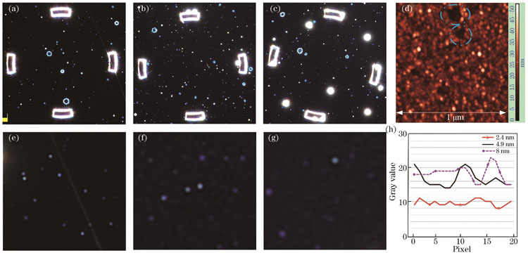
图 9. 不同RMS粗糙度值膜层表面颗粒的实测结果。(a)~(c)RMS粗糙度分别为2.4、4.9、8 nm的样片在暗场显微镜下的观察结果;(d)RMS粗糙度为8 nm的样片在原子力显微镜下的扫描结果;(e)~(g)图(a)~(c)的局部区域;(h)不同RMS粗糙度下的背景噪声曲线
Fig. 9. Detection results of particles on film surface with different RMS roughness values. (a)‒(c) Observation results of the samples with RMS roughness of 2.4, 4.9 and 8 nm under dark field microscope; (d) scanning results of the sample with RMS roughness of 8 nm under AFM;(e)‒(g) local areas of Figs. 9 (a), (b) and (c); (h) background noise curves under different RMS roughness values
5.2 偏振调控下的效果展示
取RMS粗糙度为2.4 nm的样片进行观察,旋转入射光路上的波片,改变入射光偏振态,得到的图像如

图 10. 自建系统对RMS粗糙度为2.4 nm的样片的实测结果。(a)~(c)三种不同偏振光入射下的检测结果;(d)与三图对应的颗粒信号曲线
Fig. 10. Detection results of the experimental system on the sample with RMS roughness of 2.4 nm. (a)‒(c) Detection results with three different polarized light incidence; (d) particle signal curve corresponding to Fig.10 (a), (b) and (c)
固定入射偏振态,旋转暗场接收光路上的偏振片20°,得到了

图 11. 自建系统对RMS粗糙度为4.9 nm的样片的实测结果。(a)偏振片在初始位置下的观察结果;(b)偏振片旋转20°后的观察结果;(c)两图对应的背景噪声曲线
Fig. 11. Detection results of the samples with RMS roughness of 4.9 nm by our own experimental system. (a) Detection result with the polarizer at initial position; (b) detection result after 20° rotation of the polarizer; (c) background noise curves corresponding to Figs.11 (a) and (b)
以上实验表明利用偏振调控可以降低背景噪声从而提高系统对颗粒的检测能力。对于更小颗粒的检测场合,随着颗粒变小,散射强度急剧降低,而膜层的散射强度不变,此时易将膜层散射的背景噪声当作颗粒信号,如果此时能够降低背景噪声便能降低颗粒的误检率。
5.3 颗粒检测结果
RMS粗糙度为2.4 nm的样片上100 nm颗粒的检测结果如
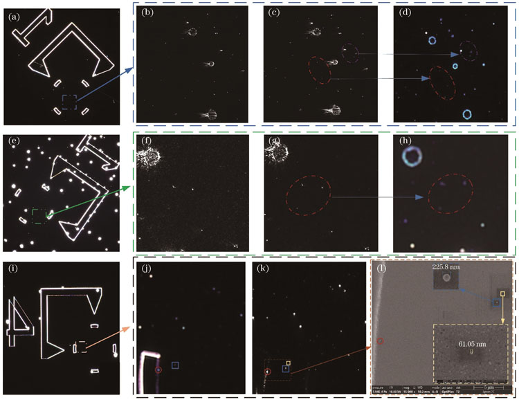
图 12. 颗粒的实测结果。(a)RMS粗糙度为2.4 nm的样片添加颗粒前的检测结果;(b)样片上添加100 nm颗粒后,暗场接收光路上不加偏振片时自建系统的检测结果;(c)自建系统调控偏振状态后的检测结果;(d)DSX1000的检测结果;(e)RMS粗糙度为8 nm的样片添加颗粒前的检测结果;(f)样片上添加100 nm颗粒后,暗场接收光路上不加偏振片时自建系统的检测结果;(g)自建系统调控偏振状态后的检测结果;(h)DSX1000的检测结果;(i)RMS粗糙度为3.4 nm的样片添加颗粒前的检测结果;(j)样片上添加50 nm颗粒后DSX1000的检测结果;(k)自建系统偏振调控后的检测结果;(l)颗粒的扫描电镜照片
Fig. 12. Particle detection result. (a) Detection results before adding 100 nm particles to the sample with RMS roughness of 2.4 nm; (b) detection results of the self-built experimental system without polarizer on the dark field receiving optical path after adding 100 nm particles; (c) detection results of the self-built experimental system after modulating the polarization state; (d) detection results of DSX1000; (e) detection results before adding 100 nm particles to the sample with 8 nm RMS roughness; (f) detection results of the self-built experimental system without polarizer on the dark field receiving optical path after adding 100 nm particles; (g) detection results of the self-built system with modulating the polarization state; (h) detection results of DSX1000; (i) detection results before adding particles to the sample with 3.4 nm RMS roughness; (j) detection results of DSX1000 after adding 50 nm particles to the sample; (k) detection results of the self-built experimental system after modulating the polarization state; (l) SEM image of the particles
RMS粗糙度为8 nm的样片上100 nm颗粒的检测结果如12(e)~(h)所示,各图含义与前文相同,由于8 nm样片较前者粗糙,能观察到背景中较为明显的“霾”现象,即背景噪声较大。经偏振调控后的检测结果如
RMS粗糙度为3.4 nm的样片上50 nm颗粒的检测结果如12(i)~(l)所示,其中
为了获得整个表面的颗粒全貌,需要对图像进行拼接。首先对初始图像进行增强、滤波操作,然后检测待拼接图像中的SURF特征点,提取每个特征点对应的特征描述向量,在匹配的特征点处估计待拼接图像的几何变换关系(在匹配过程中采用M-estimator Sample Consensus(MSAC)算法去除误匹配点,完成图像融合),最后对整图进行颗粒区域分割,统计颗粒数量。
6 结论
笔者有针对性地开展了基于金属膜层激发表面等离子体进行超衍射加工这一领域缺陷检测的相关研究工作,通过偏振调控技术抑制了背景噪声,用473 nm检测光源实测了银膜表面61 nm的PSL颗粒,避免了紫外、深紫外光刻胶在现有深紫外设备检测过程中易改性失效的问题,并且该方案具有向其他波段扩展的能力,原理上可以按光刻胶感光特性灵活选择不同的波长,在不影响光刻胶的同时提高对颗粒的检测能力。此外,本装置在进行100 nm颗粒检测时,单次曝光时间为150 μs,具有较高的检测效率。
[1] Atwater H A. The promise of plasmonics[J]. Scientific American, 2007, 296(4): 56-63.
[2] Fang N, Lee H, Sun C, et al. Sub-diffraction-limited optical imaging with a silver superlens[J]. Science, 2005, 308(5721): 534-537.
[3] Luo X G. Plasmonic metalens for nanofabrication[J]. National Science Review, 2018, 5(2): 137-138.
[4] Chang C, Chen W, Chen Y, et al. Recent progress on two-dimensional materials[J]. Acta Physico-Chimica Sinica, 2021, 37(12): 2108017.
[5] Wang J, Li Z C, Liu W N. Rigorous analysis and systematical design of double-layer metal superlens for improved subwavelength imaging mediated by surface plasmon polaritons[J]. Nanomaterials, 2022, 12(20): 3553.
[6] 李柱, 王长涛, 孔维杰, 等. 用于可见光波段切趾成像的宽带消色差超表面滤波器[J]. 光电工程, 2021, 48(5): 200466.
[7] 周毅, 梁高峰, 温中泉, 等. 光学超分辨平面超构透镜研究进展[J]. 光电工程, 2021, 48(12): 210399.
[8] 王长涛, 赵泽宇, 高平, 等. 表面等离子体超衍射光学光刻[J]. 科学通报, 2016, 61(6): 585-599.
Wang C T, Zhao Z Y, Gao P, et al. Surface plasmon lithography beyond the diffraction limit[J]. Chinese Science Bulletin, 2016, 61(6): 585-599.
[9] Luo Y F, Kong W J, Zhao C W, et al. Subdiffraction nanofocusing of circularly polarized light with a plasmonic cavity lens[J]. Journal of Materials Chemistry C, 2019, 7(19): 5615-5623.
[10] Gao P, Pu M B, Ma X L, et al. Plasmonic lithography for the fabrication of surface nanostructures with a feature size down to 9 nm[J]. Nanoscale, 2020, 12(4): 2415-2421.
[11] Poddubny A, Iorsh I, Belov P, et al. Hyperbolic metamaterials[J]. Nature Photonics, 2013, 7(12): 948-957.
[12] Beliaev L Y, Takayama O, Melentiev P N, et al. Photoluminescence control by hyperbolic metamaterials and metasurfaces: a review[J]. Opto-Electronic Advances, 2021, 4(8): 210031.
[13] Zhou R J, Edwards C, Bryniarski C, et al. White-light interferometric microscopy for wafer defect inspection[J]. Proceedings of SPIE, 2015, 9336: 93362P.
[14] Liu H Y, Sun X Q, Wang X, et al. The localized enhancement of surface plasmon standing waves interacting with single nanoparticles[J]. Plasmonics, 2021, 16(6): 2109-2116.
[15] Sun X Q, Liu H Y, Jiang L W, et al. Detecting a single nanoparticle by imaging the localized enhancement and interference of surface plasmon polaritons[J]. Optics Letters, 2019, 44(23): 5707-5710.
[16] Wang B, Tanksalvala M, Zhang Z, et al. A new metrology technique for defect inspection via coherent Fourier scatterometry using orbital angular momentum beams[J]. Proceedings of SPIE, 2021, 11611: 116110L.
[17] Kolenov D, Urbach H P, Pereira S F. Effect of polarization in evanescent wave amplification for the enhancement of scattering of nanoparticles on surfaces[J]. OSA Continuum, 2020, 3(4): 742-758.
[18] Kolenov D, Zadeh I E, Horsten R C, et al. Direct detection of polystyrene equivalent nanoparticles with diameter of 21 nm (∼λ/19) using coherent Fourier scatterometry: erratum[J]. Optics Express, 2022, 30(16): 29841-29843.
[19] 艾立夫. 基于散射光暗场显微的基片表面颗粒检测方法研究[D]. 成都: 中国科学院光电技术研究所, 2019.
AiL F. Research on particle detection method on substrate surface based on scattered light dark field microscopy[D]. Chengdu: Institute of Optics and Electronics, Chinese Academy of Sciences, 2019.
[20] 陆敏, 王治乐, 张树青, 等. 表面缺陷的偏振散射表征方法及区分原理[J]. 光学学报, 2021, 41(12): 1229001.
[21] 陈修国, 王才, 杨天娟, 等. 集成电路制造在线光学测量检测技术:现状、挑战与发展趋势[J]. 激光与光电子学进展, 2022, 59(9): 0922025.
[22] Dong J T. Line-scanning laser scattering system for fast defect inspection of a large aperture surface[J]. Applied Optics, 2017, 56(25): 7089-7098.
[23] HuangC Y, ChuR, NeskovicG. Rough film wafer sensitivity improvement using light scattering inspection system[C]∥ASMC 2013 SEMI Advanced Semiconductor Manufacturing Conference, May 14-16, 2013, Saratoga Springs, NY, USA. New York: IEEE Press, 2013: 191-193.
[25] Stover J C. Surface roughness measurements of curved surfaces by light scatter[J]. Optical Engineering, 1982, 21(6): 987-990.
[26] 唐晋发, 顾培夫, 刘旭. 现代光学薄膜技术[M]. 杭州: 浙江大学出版社, 2006.
TangJ F, GuP F, LiuX. Modern optical thin film technology[M]. Hangzhou: Zhejiang University Press, 2006.
[27] Germer T A. Angular dependence and polarization of out-of-plane optical scattering from particulate contamination, subsurface defects, and surface microroughness[J]. Applied Optics, 1997, 36(33): 8798-8805.
[28] Nahm K B, Wolfe W L. Light-scattering models for spheres on a conducting plane: comparison with experiment[J]. Applied Optics, 1987, 26(15): 2995-2999.
[29] Zhang Y H, Yang Y Y, Li C, et al. Defects evaluation system for spherical optical surfaces based on microscopic scattering dark-field imaging method[J]. Applied Optics, 2016, 55(23): 6162-6171.
[30] Cho S, Lee J, Kim H, et al. Super-contrast-enhanced darkfield imaging of nano objects through null ellipsometry[J]. Optics Letters, 2018, 43(23): 5701-5704.
Article Outline
邓泉, 赵泽宇, 林鹤, 刘玲, 李夏楚秦, 杨根森, 罗先刚. 晶圆金属表面纳米颗粒暗场检测系统设计[J]. 中国激光, 2023, 50(22): 2204003. Quan Deng, Zeyu Zhao, He Lin, Ling Liu, Xiachuqin Li, Gensen Yang, Xiangang Luo. System Design for Dark‑Field Detection of Nanoparticles on Wafer Metal Surface[J]. Chinese Journal of Lasers, 2023, 50(22): 2204003.
